Article

An Acoustic Vehicle Detector and Classifier Using a Reconfigurable Analog/Mixed-Signal Platform

by
Swagat Bhattacharyya
1,†,
Steven Andryzcik
2,† and
David W. Graham
2,*
1
School of Electrical and Computer Engineering, Purdue University, West Lafayette, IN 47907, USA
2
Lane Department of Computer Science and Electrical Engineering, West Virginia University, Morgantown, WV 26506, USA
*
Author to whom correspondence should be addressed.
These authors contributed equally to this work.
J. Low Power Electron. Appl. 2020, 10(1), 6; https://doi.org/10.3390/jlpea10010006
Submission received: 1 February 2020 / Revised: 16 February 2020 / Accepted: 18 February 2020 / Published: 20 February 2020
(This article belongs to the Special Issue CMOS Low Power Design Vol. 2)

Abstract

:
The wireless sensor nodes used in a growing number of remote sensing applications are deployed in inaccessible locations or are subjected to severe energy constraints. Audio-based sensing offers flexibility in node placement and is popular in low-power schemes. Thus, in this paper, a node architecture with low power consumption and in-the-field reconfigurability is evaluated in the context of an acoustic vehicle detection and classification (hereafter “AVDC”) scenario. The proposed architecture utilizes an always-on field-programmable analog array (FPAA) as a low-power event detector to selectively wake a microcontroller unit (MCU) when a significant event is detected. When awoken, the MCU verifies the vehicle class asserted by the FPAA and transmits the relevant information. The AVDC system is trained by solving a classification problem using a lexicographic, nonlinear programming algorithm. On a testing dataset comprising of data from ten cars, ten trucks, and 40 s of wind noise, the AVDC system has a detection accuracy of 100%, a classification accuracy of 95%, and no false alarms. The mean power draw of the FPAA is 43 μ W and the mean power consumption of the MCU and radio during its validation and wireless transmission process is 40.9 mW. Overall, this paper demonstrates that the utilization of an FPAA-based signal preprocessor can greatly improve the flexibility and power consumption of wireless sensor nodes.

1. Introduction

1.1. Wireless Sensor Networks and Acoustic Techniques

Over the past decade, the rapid rise of the Internet of Things (IoT) has facilitated the advancement of remote sensing by simplifying the design and expanding the scale of wireless sensor networks (WSNs) [1,2,3,4,5]. Yet, WSN expansion has faced bottlenecks due to the energy constraints and accessibility restrictions imposed by the remote placement of sensor nodes [1]. Thus, there is a growing demand for reliable devices with ultra-low power consumption and high wireless reprogrammability.
To achieve low power consumption, minimally preprocessed data are often transmitted to a base station for further analysis. However, frequent wireless communication can be a leading contributor to energy cost in WSNs. Another school of thought is to locally process data and only transmit relevant information. In general, there exists a tradeoff between computation and communication overhead in WSNs [6]. Nevertheless, local processing may be a more viable choice in scenarios where sensor data are sparse in relevant information content or where the necessary computational tasks can be performed at low energy cost.
Audio data are often sparse in relevant information, which makes audio sensor nodes good candidates for the local-processing approach. Audio capture and analysis inherently consumes less energy than its video counterpart, making acoustic techniques good for low-power sensing schemes [7]. Acoustic vehicle detection and classification (hereafter “AVDC”) has previously been used as a benchmark for the validation of low-power node architectures [6]. AVDC has applications in traffic monitoring and military surveillance, especially in scenarios where sensors cannot be placed in the line of sight of the classification target [2].
Vehicles, like many other objects with rotary or oscillatory components, can be identified from the frequency content of their acoustic signature. Hence, wavelet analysis, which classifies objects based on temporal frequency content, has been used in AVDC-like applications [8]. However, wavelet analysis is energy-intensive due to the involved digital computations.
Amplitude analysis is another oft-used audio processing method. It is typically executed through a thresholding scheme like the structural integrity monitor presented in [9]. Adaptive thresholding was proposed for vehicle detection in [10]. The approach taken in [11] uses an envelope detector and comparator to construct an event detector for a low-power cargo monitoring tag. Amplitude analysis affords simple, energy-efficient solutions to a multitude of problems but causes a high false alarm rate due to its low event-oriented specificity. For the AVDC task, a combination of spectral analysis and amplitude analysis could achieve good accuracy while maintaining low power consumption and simplicity.
The ability to implement training with the node out-of-the-loop would help hasten node deployment and facilitate remote reconfigurability. With the node out-of-the-loop, training can be done offline with the same reconfigurable architectures being used in the field. With this approach, system parameters can be re-adjusted in the field if more data become available, and specific adjustments can be made for individual node performance. Deployed nodes can also be repurposed for different remote-sensing tasks without the need for retrieval. Minimizing the number of programming cycles undergone by the sensor node potentially saves time and energy while extending the lifespan of the node.

1.2. Proposal, Novelty, and Overview

Digital signal processors (DSPs) are oft-used in wireless sensor nodes due to several merits. For one, DSPs can be readily repurposed for a wide assortment of tasks, providing great benefit to node flexibility and programmability [6]. Additionally, digital systems have good immunity to electrical noise and environmental fluctuations, which make them a reliable choice for long-term applications. Recent applications of digital signal processing include a low-power feature extractor for speech recognition [12] and a front-end for an electrocardiogram acquisition system [13]. DSP energy-efficiency has historically followed Gene’s Law, doubling every 18 months due to the power savings afforded by rapid technology scaling [14].
Yet, analog-to-digital converters, which are at the heart of DSP-based sensor nodes that interface with analog sensors, have not kept up with Gene’s Law [14] and are still a dominant contributor to overall power draw in digital sensor nodes [15]. Improvements in DSP energy-efficiency are becoming infrequent as technology scaling becomes physically difficult and prohibitively expensive. Resource-constrained digital systems may suffer from high latency as well, which can be a concern in certain scenarios [16].
In contrast, analog signal processors (ASPs) can directly interface with analog sensors, forgoing the need for analog-to-digital converters. ASP-based solutions offer real-time, low-power signal processing and often require less infrastructure than their digital counterparts. Analog electronics endow designers with a rich assortment of powerful computational components at ultra-low energy cost [17,18]. In fact, [14] noted that ASP energy-efficiency has historically led DSP technology scaling by 20 years.
These are several reasons why analog circuits are used in sensor interfaces like the capacitive sensing front end demonstrated in [19] and the delay line for ultrasonic imaging demonstrated in [20]. ASPs are also widely used in biopotential acquisition and analysis systems, finding recent applications in the current-mode front-end proposed in [21] and the electrocardiogram feature detector proposed in [22]. There have also been recent demonstrations of ASPs in machine learning, such as the convolutional neural network processor shown in [23] and the framework for computing Gaussian kernels shown in [24].
Yet, analog circuits can be susceptible to electrical noise and environmental changes. Analog electronics are also ill-suited for certain tasks (such as radio transmission or sequential logic). It may be more synergistic to use a combination of analog and digital electronics for a general-purpose node architecture. Hence, this paper proposes a hybrid node architecture comprising of an always-on, mixed-signal processor (MSP) and a microcontroller unit (MCU) that is only awoken when a significant event is detected by the MSP. In this way, the intrinsic device physics of analog components are leveraged to perform computations that would inherently require more power on fully digital platforms while still retaining the abilities to wirelessly network and perform sophisticated digital computation. [1,6,25] have previously shown that this type of configuration can facilitate significant power savings.
Although this paper expands on the work described in [6], it differs in a few aspects from previous works that offered solutions to the AVDC problem. Related works utilized application-specific integrated circuits (ASICs) [1,6,9,10,25]. ASICs offer superb performance, ultra-low power consumption (especially with an integrated MSP), and good robustness. However, ASIC development is time-consuming and ASIC-based solutions can be limited in their ability to handle future changes to procedures or overall tasks. These issues are mitigated in this paper by using a low-power field-programmable analog array (FPAA). Compared to an ASIC-based solution, an FPAA-based solution can leverage mixed-signal computation and a reconfigurable architecture for a more expansive scope.
The reconfigurable analog/mixed-signal Platform (RAMP) introduced in [26] is the base for the preprocessing circuitry in this paper. By utilizing the RAMP, which contains a custom-designed FPAA at its heart, a sensor node with immense post-deployment reconfigurability, flexibility, and versatility can be achieved. As a consequence of using the RAMP, the event-detection stage of the AVDC system proposed in this work is different from that used in [6], which was based on an analog ASIC. In this work, floating-gate transistors (FGs) were used for comparator threshold generation instead of digital potentiometers, a lookup table (LUT) was used for template matching instead of a complex programmable logic device, and a panStamp MCU was used for transmission of the final decision instead of a TelosB digital platform. The subcircuits used in the spectral-analysis stage of the MSP also have different topologies than their counterparts in [6], and a digital debouncing circuit is introduced to the event-detection stage. A comparison between the results of this work and [6] highlight the improvements in power consumption and accuracy that are possible by using a reconfigurable system rather than an ASIC.
To take full advantage of the increased precision afforded by generating comparator thresholds with FG-transistor-based circuits, a new training algorithm is proposed in this paper. The training algorithm used in [6] used brute enumeration of comparator thresholds, keeping the MSP in-the-loop throughout the entire training process. This methodology is only practical if threshold increments are coarse; hence, the methodology proposed in this paper uses a two-step, continuous-optimization procedure to determine comparator thresholds and requires significantly less communication with the MSP.
In summary, this paper evaluates the performance of a reconfigurable analog system within the context of a vehicle detection and classification application. The remainder of the paper is as follows: In Section 2, the infrastructure of the RAMP is discussed. The topology of the AVDC circuit is explained in Section 3. Section 4 discusses the process of training the AVDC system. Section 5 demonstrates the performance of the AVDC circuit in comparison to historical work. Finally, Section 6 offers concluding remarks.

2. System Architecture

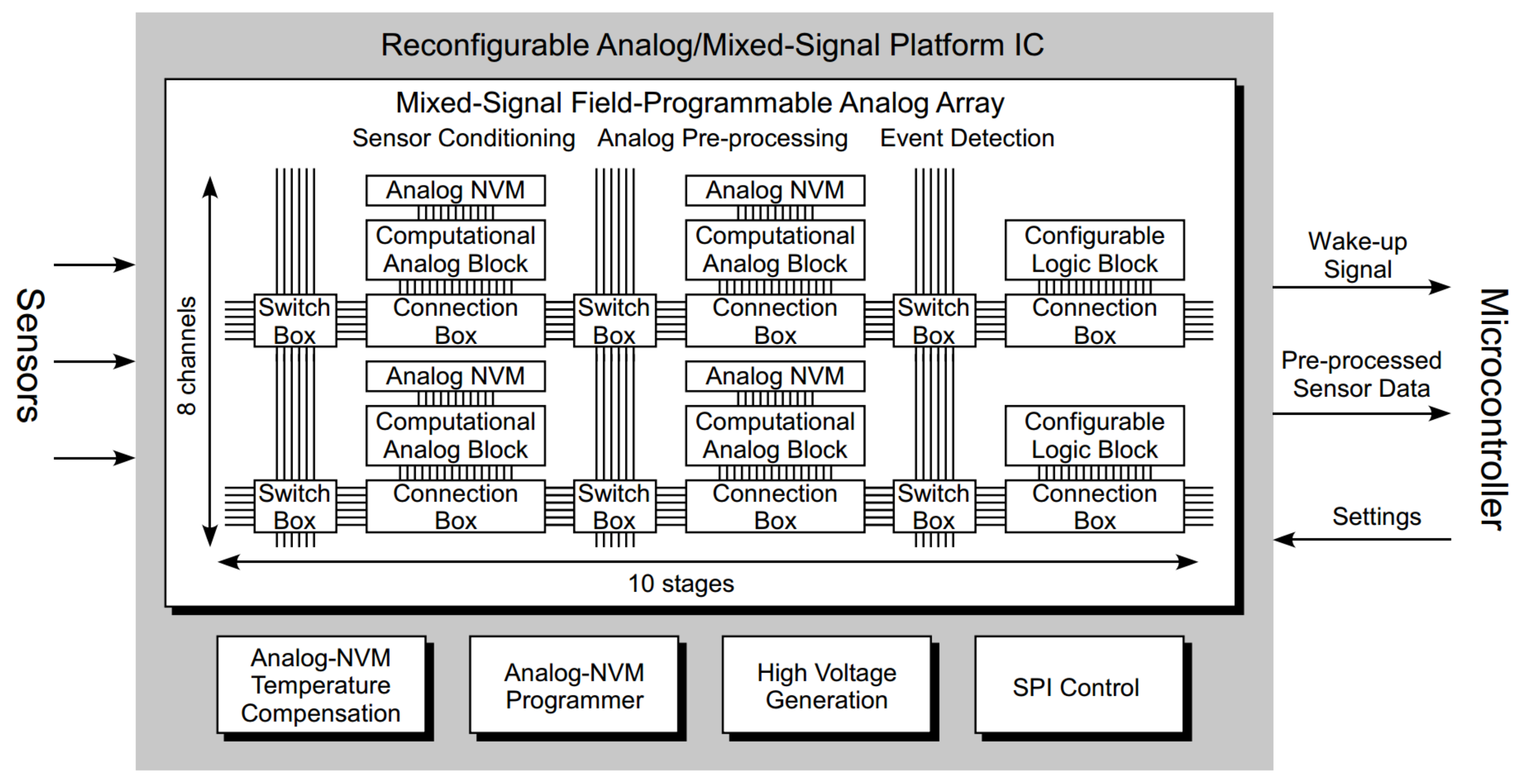
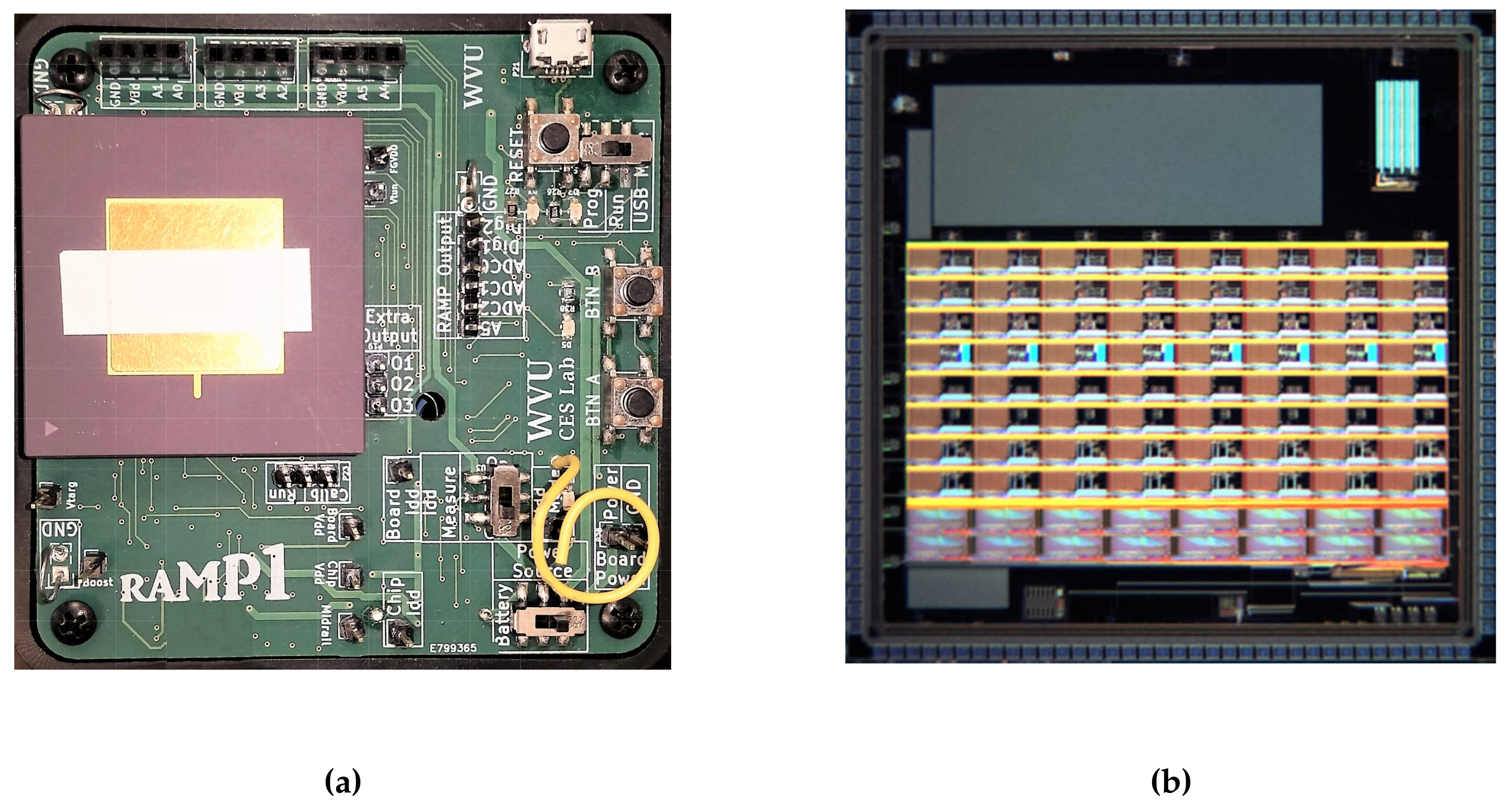
2.1. Reconfigurable Platform

A field-programmable analog array (FPAA) is a reconfigurable integrated circuit (IC) that is the mixed-signal analogue to a field-programmable gate array (FPGA); while FPGAs allow for post-fabrication synthesis of digital circuits, FPAAs allow for the post-fabrication synthesis of analog circuits [27,28,29]. FPAAs can be used to synthesize common circuits such as amplifiers or filters, making them useful for sensor interfacing applications. The reconfigurable, analog architecture of an FPAA allows for both general-purpose analog signal processing and complex application-driven signal-processing tasks [30].
The RAMP (described at length in [26]) leverages a custom-designed FPAA structure to provide an abundant number of signal processing and computational elements. The RAMP consists of ten stages of computational analog blocks (CABs), including specific stages for spectral-analysis, transconductors, sensor interfacing, mixed-signal-processing, digital computation, and general transistors. Each of the ten stages are replicated to create eight independently reconfigurable channels.
Of primary importance for this AVDC application are the spectral-analysis, mixed-signal, and digital stages. The spectral-analysis CABs contain bandpass filters (BPFs), peak detectors, adaptive-time-constant filters, and operational transconductance amplifiers (OTAs). The mixed-signal CABs contain comparators, sample and holds, pulse generators, timers, and starved inverters. The digital stages contain LUTs and JK flip-flops.
Signal routing in the RAMP is achieved via two programmable switch domains: “switch boxes” and “connection boxes” (as shown in Figure 1). These programmable switches are implemented using SRAM-controlled T-gates (nMOS and pMOS transistors connected in parallel to create a rail-to-rail switch). The “connection boxes” provide a crossbar switch matrix comprised of T-gates for intra-CAB routing. The “switch boxes” utilize the T-gates in a 4-way “diamond-switch,” allowing for inter-CAB connections. A desired switch configuration can be loaded into the RAMP using an on-chip serial-peripheral interface (SPI). In total, 20,380 switches are included within the RAMP [26].
CABs are connected to tunable FG current biases, allowing for the performance of analog circuits with programmable parameters (e.g., corner frequencies and gain) to be modified to fit a user-specified design constraint. The printed circuit board (PCB) that houses the RAMP can be seen in Figure 2a. The PCB includes the RAMP (die micrograph shown in Figure 2b), the MCU, and several peripherals (such as sensors, communication interfaces, and buttons/switches).

2.2. Programming Infrastructure

FGs are the building blocks of nonvolatile memory. FGs are metal-oxide-semiconductor field-effect-transistors with capacitors connected to their gate such that the gate of the transistor is floating (isolated from any DC path to ground). The charge stored on the gate regulates the current allowed through the transistor [31]. In this way, charge can be stored on the gate to create a long-term controlled current source.
Two different processes are used to apply or remove charge from an FG. Hot-carrier injection (hereafter “injection”) is used to add charge to the FG, and Fowler-Nordheim tunneling (hereafter “tunneling”) is used to remove charge from the FG [31]. Due to the high voltages required for tunneling, the RAMP only utilizes tunneling for global erasure of FGs. To perform fast, linear injection on the RAMP, FGs are individually placed into a programming structure. This structure is a continuous-time, OTA-based, negative feedback controller which compares the voltage on the control gate of the FG being injected to a target voltage. The injection target voltage corresponds to a characterized bias current that is desired from the FG [31]. After programming, FGs are connected to CABs to bias analog circuits.
Configuration of the RAMP IC is expedited by a few layers of abstraction. To synthesize a circuit on the RAMP, a user must first provide the RAMP software with the corresponding netlist. The RAMP software then estimates injection target voltages for the necessary FGs and uses simulated annealing [32] to estimate the switch activation pattern resulting in the shortest mean path among the components specified in the netlist. FG and switch domain configurations are then compressed and sent to the MCU on the RAMP development board. The MCU then communicates with the RAMP IC through SPI to place each required FG into the programming structure and inject them to their respective targets. Switch domains are configured after all FG programming is complete [26]. The RAMP IC can be reconfigured in-the-field, but any user-specified configurations will be not be operational for the duration of programming. Once the relevant FGs and switches have been programmed, the RAMP is ready to perform user-specified operations.

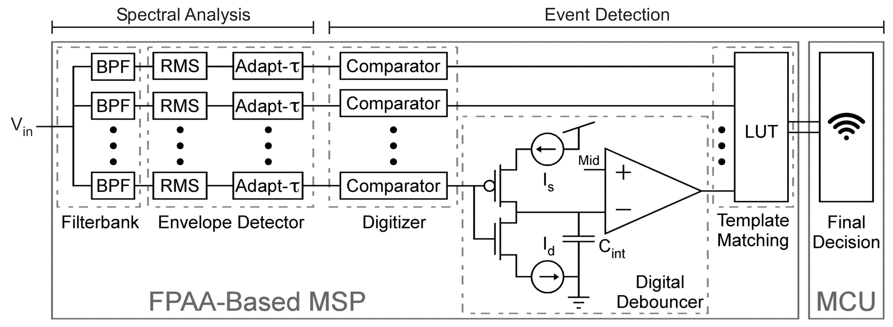
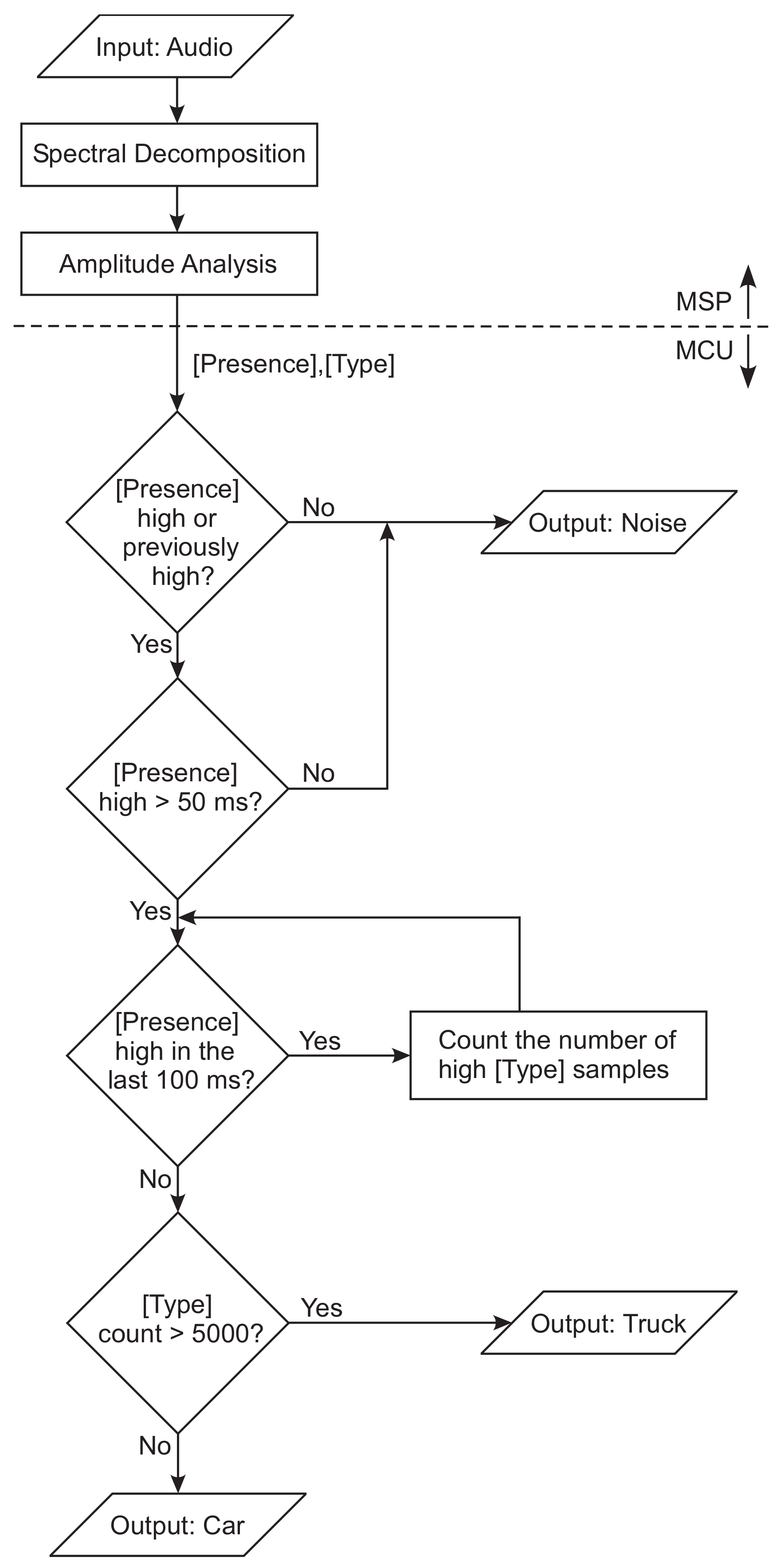
3. Vehicle Detector Configuration

As mentioned in Section 1.2, the pivotal use of an FPAA-based MSP and the implications of FPAA usage distinguish the work proposed in this paper from that on which it is based [1,6,25]. The “always-on” audio MSP constructed on the RAMP performs a combination of spectral and amplitude analyses; vehicles are identified by their instantaneous frequency content by first decomposing audio data into several frequency channels and then comparing the signal power in the frequency channels to predetermined templates. A match to the spectral template for a vehicle will wake the MCU from its low-power sleep mode. The AVDC system leverages the following signal-processing steps:
Spectral-Analysis Stage:
  • Spectral decomposition using a filterbank of bandpass filters (BPFs)
  • RMS envelope estimation using a bank of root-mean-square (RMS) detectors cascaded with a bank of ripple-smoothing, adaptive-time-constant (adaptive- τ ) lowpass filters
Event-Detection Stage:
  • Digitization using a bank of comparators
  • Digital “debouncing” using a starved inverter
  • Template matching using a LUT
  • Final decision transmission using a panStamp MCU
Figure 3 shows a block diagram of the AVDC system, and the various signal-conditioning steps of the MSP are discussed in more detail in the subsequent subsections.

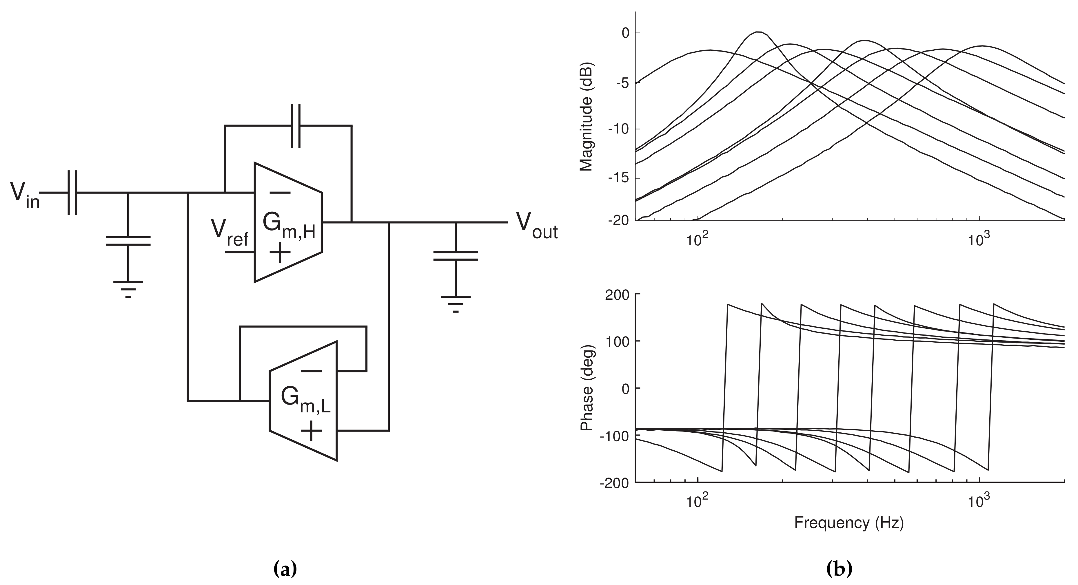
3.1. Spectral Decomposition

OTA-based BPFs, shown in Figure 4a, are utilized in a filterbank to decompose the input audio. The BPFs used in the RAMP are based on a design demonstrated in [33], and they have the benefit of independently adjustable corner frequencies. The corner frequencies of a BPF is set by tuning the transconductances of its constituent OTAs via FG current biases.
The filterbank is initially constructed with eight BPFs configured in a half-octave spacing from 77 Hz to 1113 Hz. Although the spacing between filters in adjacent channels and the exact corner frequencies can be tuned precisely [33], this level of precision is found to be of low importance for the AVDC proposed in this paper—the training algorithm proposed in Section 4b finds that a few channels contain redundant information. These redundant channels are removed from the spectral-analysis stage of the final AVDC system. Figure 4b exhibits the frequency response of the initial filterbank. To minimize the output distortion of BPFs, the range of the input to V i n should be properly scaled with the mean at midrail, and V r e f should be referenced to midrail.

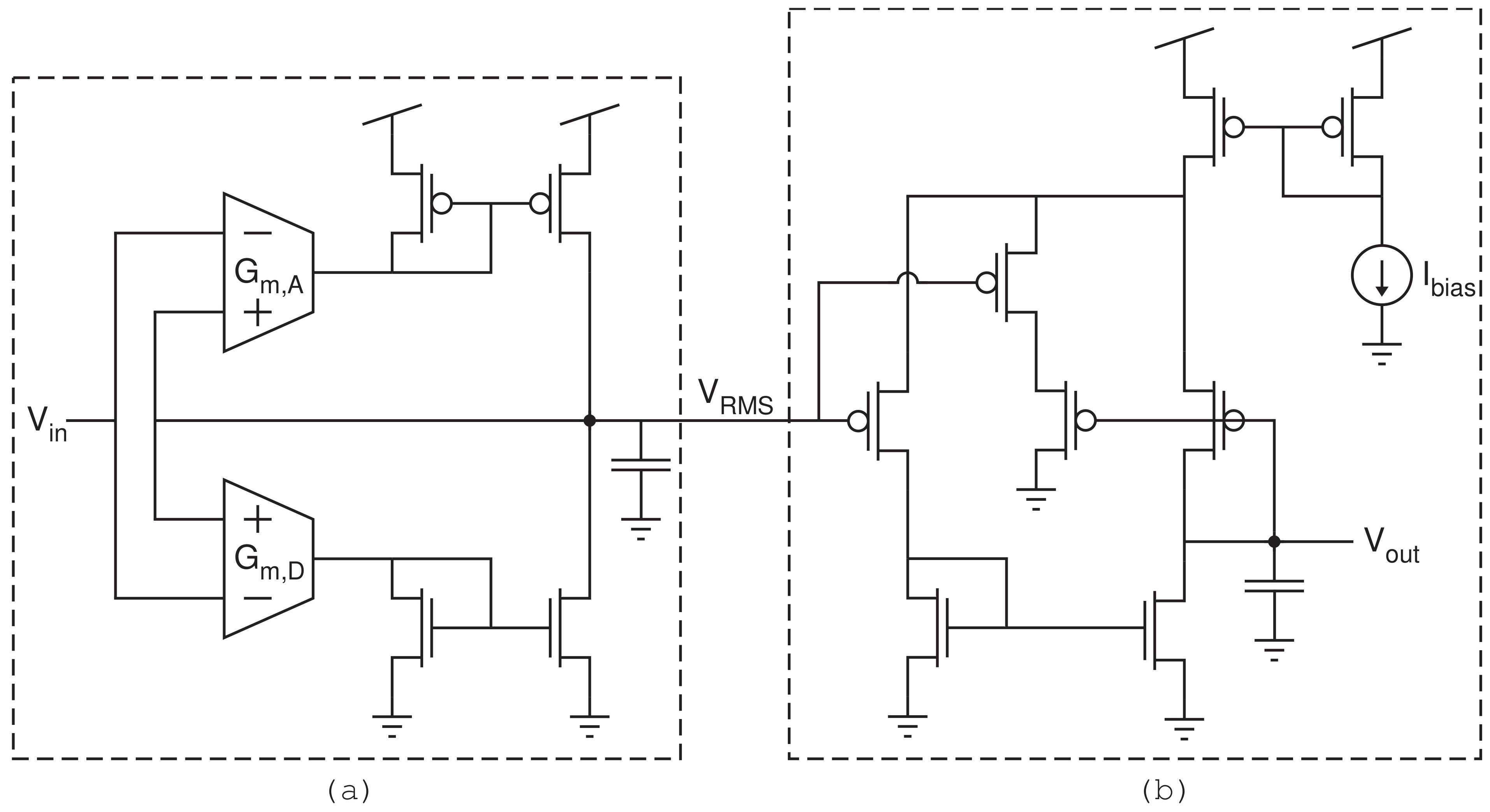
3.2. RMS Envelope Estimation

After obtaining the frequency decomposition, it is desirable to estimate the RMS envelopes of the BPF outputs to assess the instantaneous signal power in each frequency band. The peak detector described in [34] is biased as an RMS detector to perform this task. The RMS detector depicted in Figure 5a, has two independently adjustable parameters, attack rate ( G m , A ) and decay rate ( G m , D ), which correspond to the transconductances of the constituent OTAs. Adjustment of OTA transconductances also changes the output ripple of the RMS detector. The RMS detector operates like an asymmetric integrator whose output is given by
d V R M S d t G m , A ( V i n - V R M S ) , V i n > V R M S G m , D ( V i n - V R M S ) , V i n V R M S
where V i n and V R M S denote the input and output of the RMS detector, respectively.
Despite careful tuning, the RMS detector output will invariably contain some ripple, especially if an accurate envelope estimate is desired. Thus, a bank of adaptive- τ lowpass filters based on the topology presented in [34] is implemented for ripple rejection. At its core, the adaptive- τ , shown in Figure 5b, is an OTA-based lowpass filter. However, the OTA used in an adaptive- τ filter is designed to have a transconductance that increases with increasing input amplitude [34]. Hence, the time constant of the adaptive- τ filter decreases with increasing input amplitude.

3.3. Digitization

The smoothed RMS envelopes are digitized using a bank of comparators. RAMP comparators have built-in hysteresis, which aids in producing a steady LUT output despite residual noise from the spectral analysis stage. Comparator reference voltages are generated by using FGs to source or sink current through resistors. The comparator architecture in the MSP (depicted in Figure 6) consists of a differential amplifier cascaded with an inverter and an “edgifier” circuit. The edgifier circuit was proposed in [35] and uses starved inverters to accelerate the rising and falling edges of its input signal, making it useful for the digitization of slow analog signals.

3.4. Digital Debouncing

For certain channels (notably the highest frequency channel), the hysteresis inherent to a RAMP comparator is insufficient to generate a steady digital input to the LUT. Continual oscillations in the LUT input may cause excessive querying and lead to unwanted power consumption. A digital debouncing circuit (shown in Figure 3) is used to mitigate this issue. To incite a state change in the output, this debouncing circuit requires that the input signal maintain its digital state for a minimum amount of time. This minimum time requirement for the debouncer is analogous to the “setup time” requirement of a D-latch. The digital debouncing circuit is constructed by cascading a time-voltage conversion circuit with a comparator referenced to midrail. More particularly, the time-voltage conversion circuit is an asymmetrically starved inverter with the output connected to a capacitor. This implementation allows for the “setup times” necessary for the “high” or “low” state to be independently adjusted. If the voltage on the capacitor is near either supply rail prior to an input state change, the “setup time” of the debouncer can be approximated as follows:
t s e t u p M i d · C i n t I s , when input transitions from 1 0 M i d · C i n t I d , when input transitions from 0 1
The constants used in Equation (2) are labeled in Figure 3.

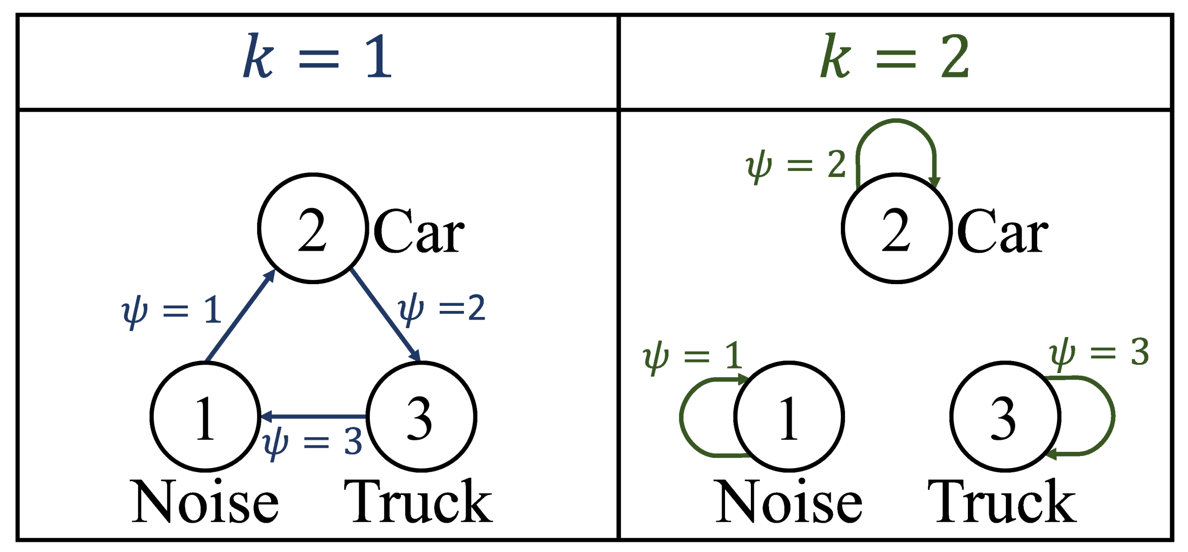
3.5. Template Matching

Once stable comparator outputs are generated, a LUT is used to match comparator activation patterns to one of the three vehicle classes considered in this paper: “noise/no car,” “car,” and “truck.” Due to chip real-estate considerations, the LUT fabricated on the RAMP is a digital framework with six inputs and two outputs that checks compliance with Boolean expressions; hence, the LUT is configured to use one output to assert vehicle presence and another output to assert vehicle type (i.e., if a truck is present). To configure a LUT, the RAMP software decompiles the necessary Boolean expressions into logical tables that are then stored in the two SRAM arrays comprising the LUT. When the LUT receives an input, it asynchronously queries the SRAM cells with the corresponding addresses to determine the outputs. Figure 7 presents a block diagram of the LUT architecture.

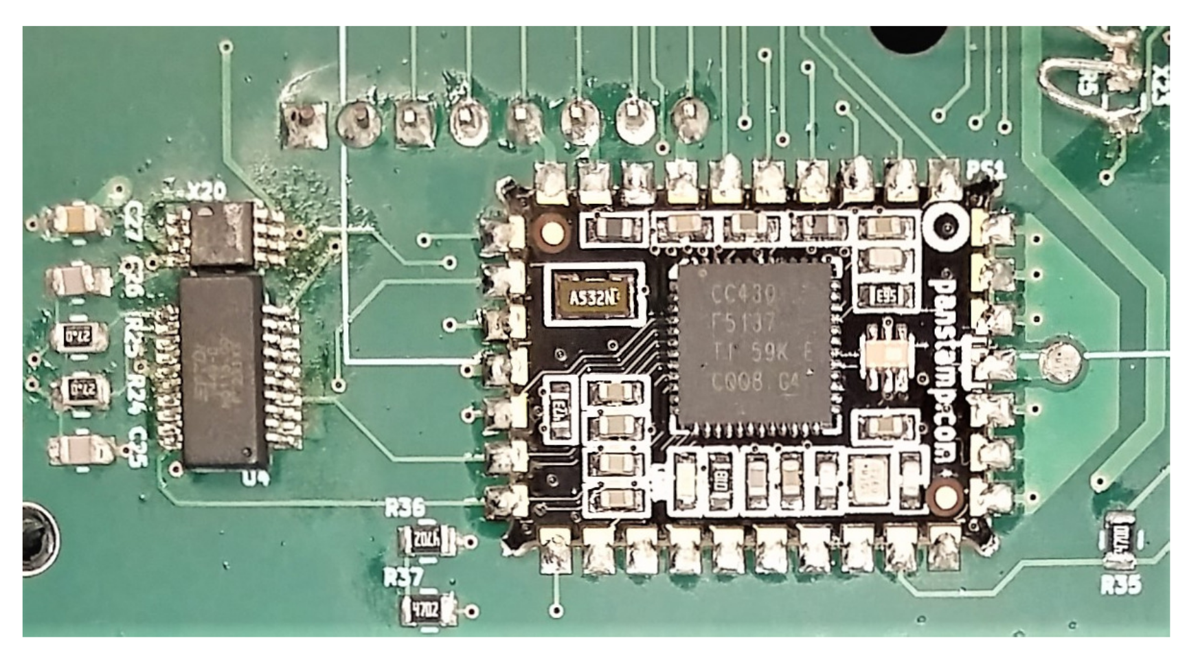
3.6. Final Decision Transmission

The preliminary decision made by the MSP is susceptible to errors due to wind noise and differences between approaching, present, and receding vehicles. Differences in vehicle size and proximity can lead to scenarios where the LUT incorrectly identifies the vehicle class. Thus, an MCU is used to verify the decision of vehicle presence by implementing the decision-accumulation scheme demonstrated in [6]. In the decision-accumulation scheme, the LUT output that asserts the presence of a vehicle is used as an interrupt or “wake-up” pin for the MCU. Once the LUT has generated an interrupt on the “vehicle presence” pin, the MCU wakes up and records both outputs from the LUT. The MCU continues sampling the LUT output until the LUT’s “vehicle presence” pin remains low for 100 ms. This additional pause helps confirm that the vehicle that triggered the interrupt has moved out of the range of the audio sensor.
The MCU then decides the vehicle class. If the LUT’s “vehicle presence” pin has been asserted for a minimum of 50 ms, the MCU decides that a vehicle is present. Otherwise, the MCU decides that the LUT has false triggered, and it returns to its low-power sleep mode. If a vehicle is present, the MCU must activate its radio transmission module to send the final decision results to a base station. However, before radio transmission, the MCU determines the vehicle type by comparing the number of samples for which the LUT’s “vehicle type” pin has been asserted to a threshold. If this threshold (which is estimated to be 5000 samples using basic training data statistics) is exceeded, the vehicle is classified as a truck; otherwise, the vehicle is classified as a car. The MCU decision-making process is summarized in Figure 8.
The panStamp NRG 2 [36] MCU was used in this work for its IoT capabilities, small form factor, and low power consumption. Despite measuring 1.6 cm by 2.2 cm, the panStamp NRG 2 has 32 kb of flash memory, a low sleep current of 1.5 μ A, a maximum radio transmission power of 12 dBm, and AES encryption capabilities. The panStamp not only enables transmission of the final MCU decision, but it also facilitates wireless reconfiguration of the RAMP IC. A photograph of a panStamp NRG 2 soldered onto the backside of the RAMP PCB is displayed in Figure 9.

4. Classifier Training

4.1. Data Preparation

Audio data preparation is the first step in the AVDC training process. The audio data used in this paper were collected previously in [16]; the data are ten-second audio clips (sampled at 4 kHz) from 20 cars and 20 trucks as well as 80 s of wind noise. Truth vectors indicating the presence and class of each vehicle were constructed via human inspection. The normalized audio and their respective truth vectors were randomly concatenated into a training and testing dataset with the same size and class composition. The training dataset was passed through the spectral-analysis stage of the AVDC system. The output stream from the adaptive- τ filter in each channel was recorded via a National Instruments 6259 data acquisition card and then imported into MATLAB® to be used in the threshold estimation procedure, as described in the next two subsections. A spectrogram demonstrating the output of the spectral-analysis stage in response to the testing dataset is shown in Figure 10 for reference.

4.2. Comparator Threshold Optimization

Once the data have been prepared, training the AVDC system entails configuring the event-detection stage of the MSP. The first step in the configuration of the event-detection stage, and the focus of this subsection, is the selection of comparator reference voltages (hereafter, “comparator thresholds”). On the RAMP, comparator threshold voltages are generated by using FGs to source or sink current through resistors. These threshold voltages should be selected such that comparator activation patterns (hereafter, “codewords”) are indicative of a specific vehicle class: (1) noise, (2) car, or (3) truck. Hamming distance, which is the minimum number of bit replacements required to match two binary strings, is a good measure of the similarity between two codewords. Hence, comparator thresholds (denoted by τ ) are selected to maximize the mean Hamming distance between codewords triggered by different vehicle classes (denoted by M 1 ) and to minimize the mean Hamming distance between codewords triggered by the same vehicle class (denoted by M 2 ). These criteria can be phrased as a multiobjective nonlinear programming problem. In this paper, maximization of M 1 is prioritized to reduce false alarms and misclassification, which cause unnecessary energy expenditure.
As noted in Section 1.2, it is desirable to keep the MSP out-of-the-loop for most of the training process to improve the training rate, reduce the degradation of FGs, and facilitate post-deployment adjustments. The event-detection circuits in the MSP are well characterized, so empirical measurements of spectral-analysis stage outputs can be utilized in software simulations to estimate configuration parameters for the event-detection stage of the MSP. These parameter estimates can be easily “ported” back to the RAMP for implementation in hardware. Hence, this optimization problem is solved with a two-step, lexicographic approach [37] using the MATLAB® fmincon solver and the interior-point algorithm.
Lexicographic approaches are multiobjective optimization strategies that sequentially optimize a series of objectives in order of decreasing priority. Lexicographic approaches can be used to obtain Pareto-optimal solutions [38]. The optimization problem proposed in this paper, has two objectives, M 1 and M 2 . In the first solution step, M 1 is maximized while M 2 is constrained by the relaxed boundary condition M 2 T a r :
M 1 M a x = max M 1 ( τ ) s . t . τ l b τ τ u b M 2 ( τ ) M 2 T a r
In Equation (3), τ l b and τ u b denote the bounds on the comparator thresholds and are set to be the minimum and maximum output voltage from each channel of the spectral-analysis stage, respectively.
In the second solution step, the “argument” τ of the “minimum” of M 2 is sought:
arg min τ M 2 ( τ ) s . t . τ l b τ τ u b M 1 ( τ ) ( 1 - ϵ ) M 1 M a x
where the optimum from the first problem ( M 1 M a x ) is relaxed by a factor of ϵ (typically around 10%) to act as a constraint on the value of M 1 for acceptable solutions. Objective functions M 1 and M 2 are computed by weighting the mean Hamming distance between each pair of codewords triggered by the relevant comparison classes by a factor that is indicative of the specificity of the codeword. Defining the objectives in this manner rewards codewords for their specificity to a particular vehicle class and for their distinctness from codewords triggered by other vehicle classes. The underlying formula for computing M 1 and M 2 can be written as M k for k { 1 , 2 } :
M k ( τ ) = 1 3 ψ = 1 3 G ( P ψ , 1 , k , P ψ , 2 , k ) H e T G ( P ψ , 1 , k , P ψ , 2 , k ) e
Where P : , : , 1 = 1 2 2 3 3 1 and P : , : , 2 = 1 1 2 2 3 3
In Equation (5), ∘ denotes the element-wise (Hadamard) matrix product, e denotes the 256 × 1 all-ones vector, H denotes the 256 × 256 matrix indicating the Hamming distance between pairs of binary codewords, and P denotes the three-dimensional matrix representing the required class comparisons. Figure 11 visually illustrates the class comparisons represented in P and the indexing scheme used in Equation (5). G represents the sparse matrix containing the occurrence frequency of each codeword comparison, which, in turn, is indicative of the class-specificity of the code words. G is computed using the following expression:
G ( P ψ , 1 , k , P ψ , 2 , k ) = F T ( P ψ , 1 , k , ) F ( P ψ , 2 , k , )
where F ( m , * ) denotes the mth row of F, a 3 × 256 matrix whose first, second, and third rows indicate the number of times each codeword (ordered by decimal value) is expected to occur when noise, cars, or trucks, respectively are present. Codewords are, in turn, estimated from τ and the output from the spectral-analysis stage of the MSP. The thresholds found through the optimization procedure proposed in this section are mapped to current biases using the characterization models of the relevant FG current sources and sinks.

4.3. Lookup Table Configuration
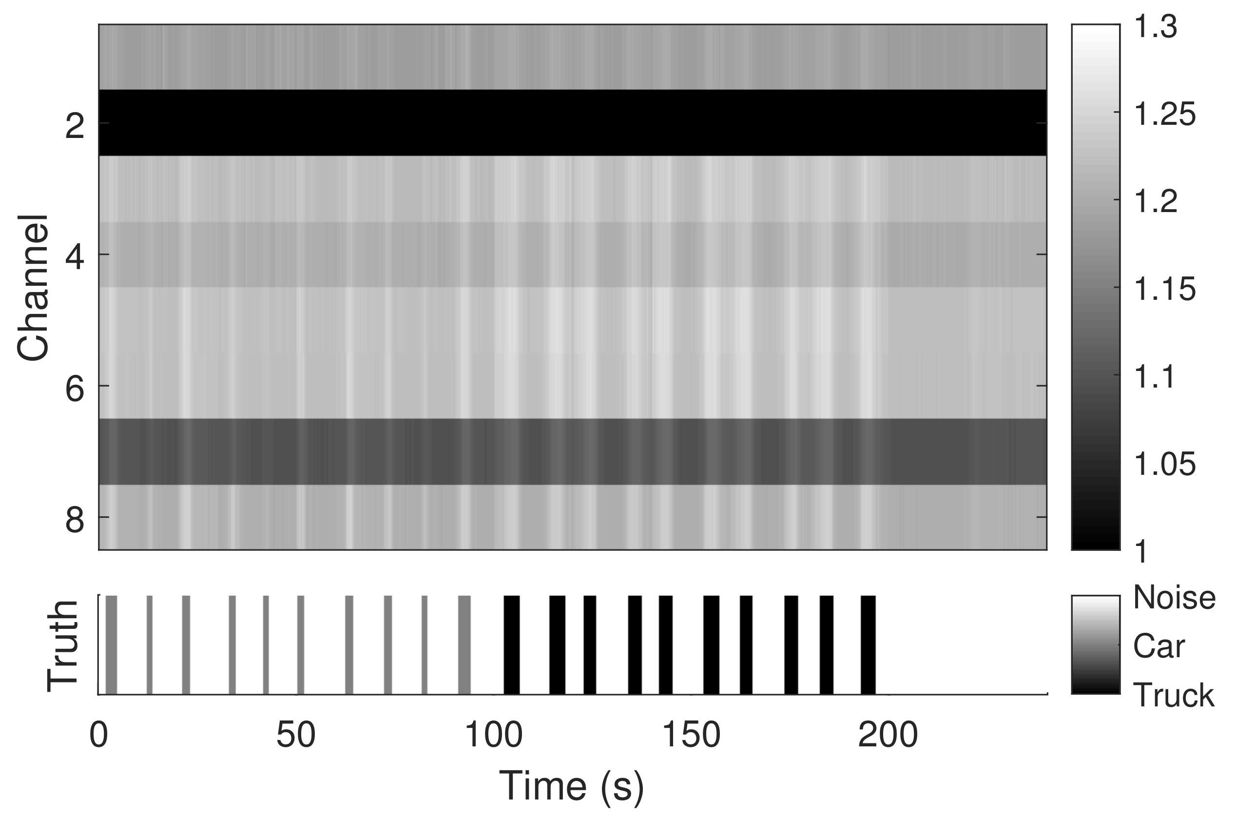
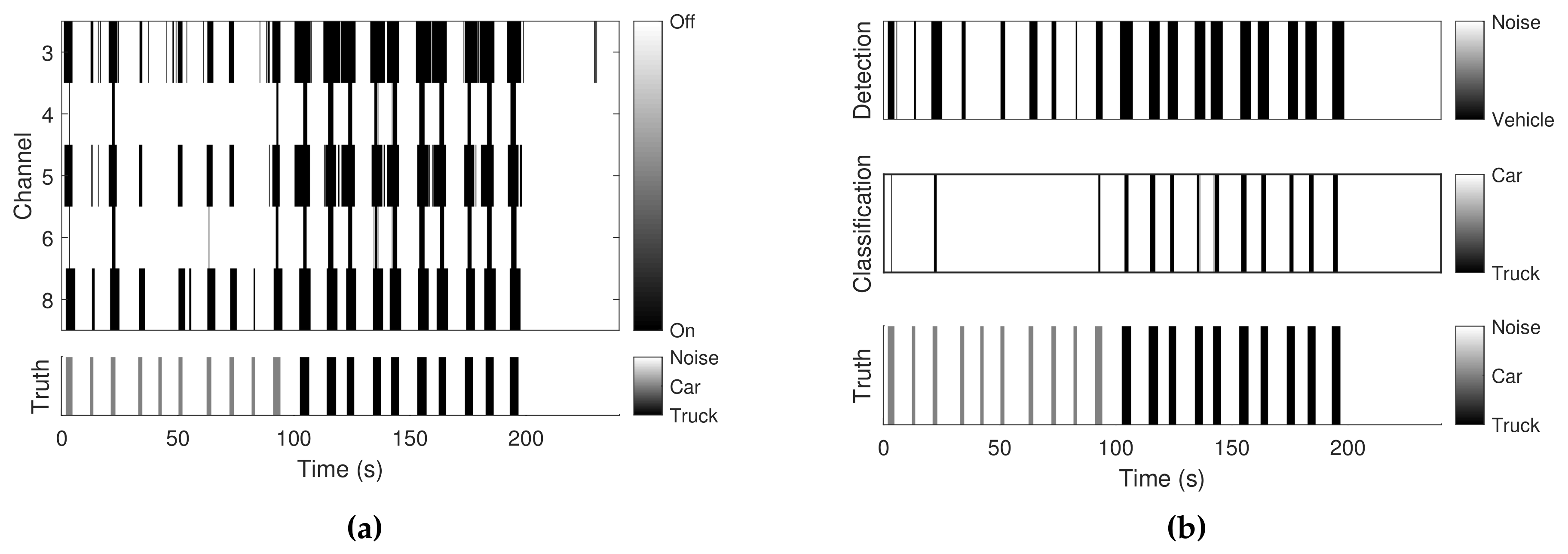
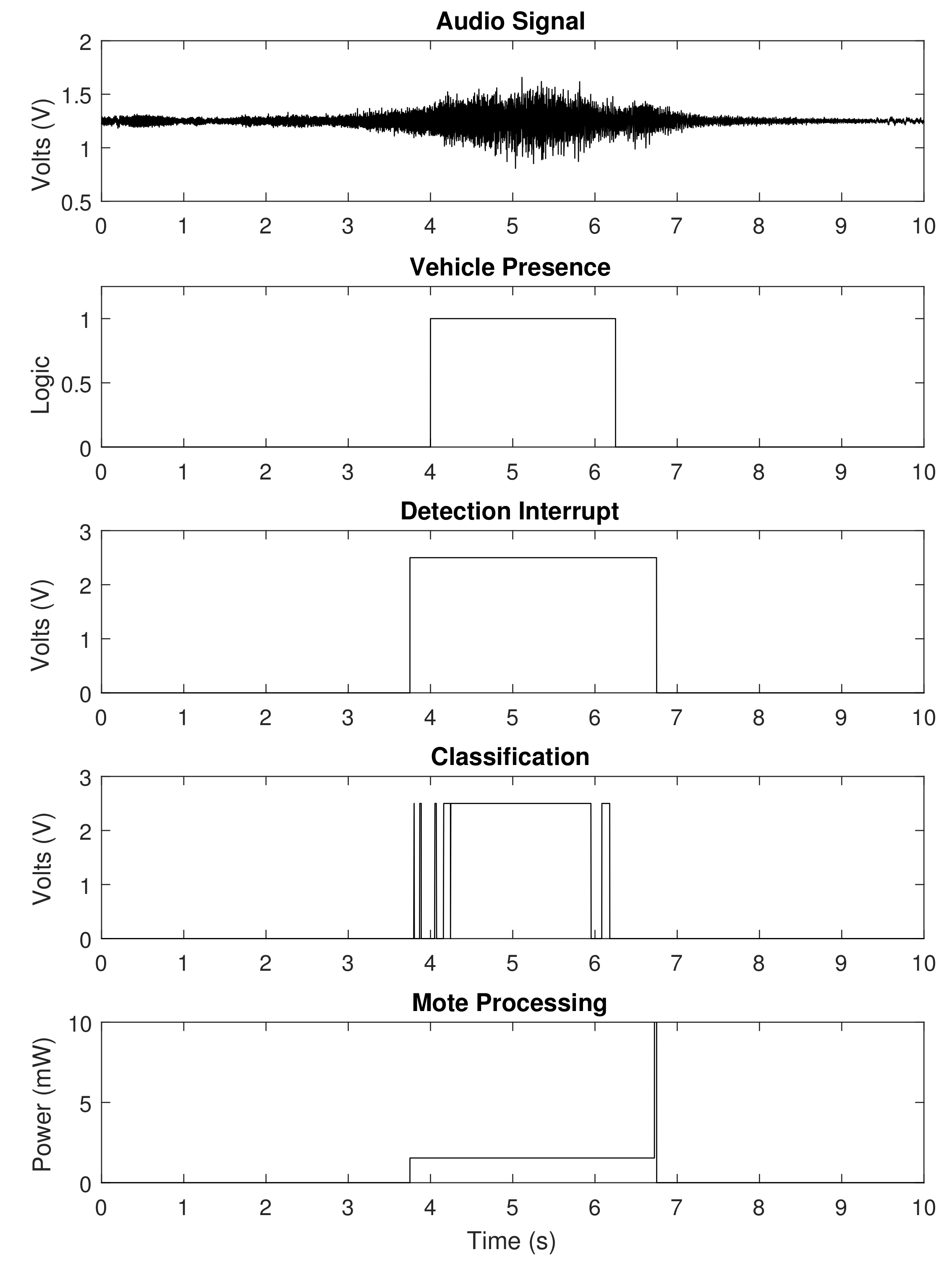
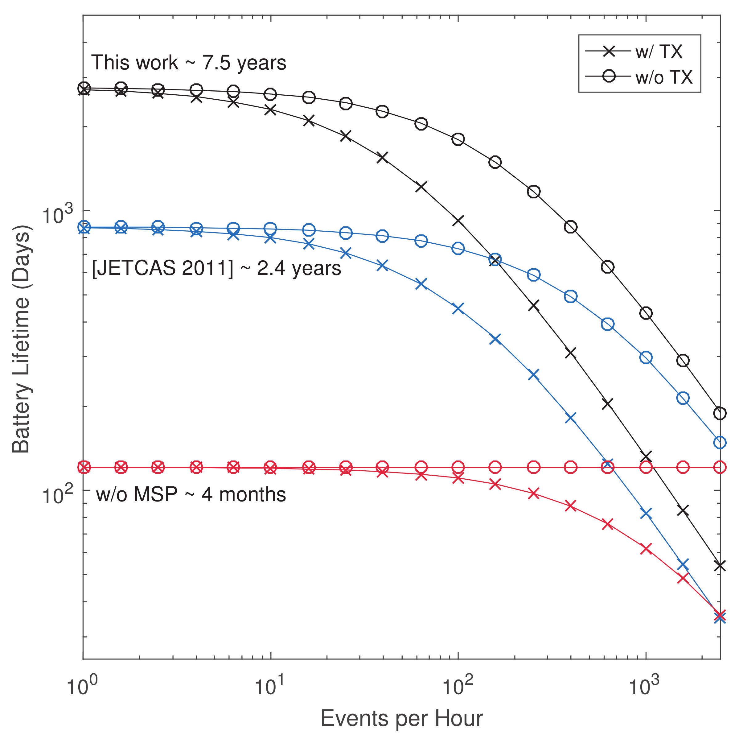
After threshold estimation, a LUT is configured such that the first output indicates vehicle presence and the second output indicates vehicle type. The RAMP contains 16 LUTs, each with six inputs and two outputs, that are available for usage in the AVDC. The flexible signal routing granted by the RAMP enables LUTs to be arrayed to obtain a variety of input–output combinations. However, we found that the LUTs did not need to be arrayed in this work; a few frequency channels contained redundant information, and the threshold selection algorithm placed the comparator thresholds for these channels near the lower or upper bounds ( τ l b or τ u b ). As a result, redundant channels had a mostly stationary comparator activation pattern and were pruned to preserve resources. The final AVDC system in this paper uses five frequency channels.
In this work, the number of nonredundant frequency channels is tractable, and comparator activation patterns are defined (where certain comparators generally activate when a vehicle is present, and other comparators generally activate when a truck is present). Hence, after the comparator threshold values have been determined by the optimization procedure, LUT Boolean expressions can be readily found via observation of the resulting codewords. Table 1 shows the percentage of codewords that belong to each vehicle class that also satisfy the Boolean templates used to configure the LUT. Figure 12a shows the codewords in response to the testing dataset, and Figure 12b demonstrates the output of the final configuration of the LUT to the testing dataset. Table 1 and Figure 12 both indicate that the performance of the LUT alone is satisfactory for vehicle detection yet unsatisfactory for vehicle classification, thus motivating the use of an MCU to interpret the output of the LUT and bridge lapses in LUT performance.
If there are a greater number of nonredundant channels or if the data contain a greater number of vehicle classes, more elaborate techniques may be necessary for LUT template selection. In such a scenario, it may be possible to leverage multiclass classification algorithms [39] to aggregate codewords into their respective vehicle classes and then use logic minimization methods to resolve the final LUT templates.

5. Results

After the training procedure, no changes are made to the AVDC system. Figure 13 shows the process of making a vehicle detection, starting from the raw audio signal from the sensor. The label for vehicle presence is shown below the input audio signal to give an idea of when the vehicle is near the microphone. “Detection Interrupt” indicates that a vehicle has been detected by the MSP. The “Classification” output from the LUT is used to implement the decision-accumulation scheme described in [6]. Once the MCU makes the final decision on the vehicle type, a radio transmission is sent (which is registered as a spike in power draw).
The MCU, which consists of the microcontroller and its peripheral devices (e.g., the radio transmitter), can operate in three distinct states. Each state’s power consumption is listed in Table 2. The first state is “sleep mode.” Sleep mode is the low-power state of the MCU when it is monitoring a digital interrupt pin for a vehicle detection from the LUT. When an interrupt has been sent from the LUT, the MCU enters the second state: “wake mode.” In wake mode, the MCU powers up to make the final decision pertaining to vehicle presence and type. If the MCU decides that a vehicle is present, it enters the third state: “radio mode.” Otherwise, it returns to sleep mode. Radio mode is the state in which the MCU’s radio transmitter is enabled to broadcast vehicle detections and classifications. Of the three modes, radio mode is the highest in power consumption, so the MCU immediately returns to sleep mode after the radio transmission is complete.
The testing data described in Section 4 were utilized to evaluate the performance of the trained AVDC system. Like the training data set, the testing data set consists of ten car samples, ten truck samples, and 40 s of wind noise. The detection and classification results of the trained AVDC for the testing dataset are shown in Table 3. The system proposed in this paper achieved a detection accuracy of 100% and a classification accuracy of 95% (one car was misidentified as a truck). The system had no false alarms during the 40 s of wind noise. False alarms cause the MCU to enter wake mode and possibly radio mode. Hence, each false positive contributes to energy consumption, which decreases the overall lifetime of a resource-constrained sensor node.
Table 3 also includes comparisons to [6], which presented results from a system with a similar analog/mixed-signal processing chain but built as an application-specific device. Since the audio data and class labels used in both papers are identical, and the signal processing circuits share some similarities (similarities are summarized in Section 1.2), comparisons to the work presented in [6] can provide a fair testimony of the merits of employing a reconfigurable system over an ASIC. In comparison to [6], which reported a classification accuracy of 80% for cars and four false positives, the AVDC presented in this paper has a higher classification accuracy for cars and no false positives.
To demonstrate the power savings of the AVDC system, Figure 14 compares battery lifetime in three scenarios—(1) this work, (2) previous work utilizing an ASIC-based MSP [6], and (3) a system with a purely digital implementation. Figure 14 shows the advancements that were made by [6] compared to an all-digital implementation, increasing the estimated lifetime from 4 months to 2.4 years. Figure 14 also shows the improvements of this AVDC system over [6], increasing the estimated lifetime from 2.4 years to 7.5 years. Additionally, Figure 14 predicts each case for both radio transmission (w/ TX, for real-time systems that need to transmit on each event occurrence) and no radio transmission (w/o TX, for data-logging systems that do not need to transmit on each event occurrence).
Other recent advances in acoustic classification systems have shown high accuracy with low power consumption. While different in application, the voice activity detectors described in [40,41,42] provide useful comparisons in terms of acoustic processing. The voice activity detector presented in [40] reports an accuracy of 89% while consuming 6 μ W. Another voice activity detector constructed from an analog filterbank feeding into a neural network reports approximately 85% accuracy while consuming only 1 μ W [41]. A voice activity detector utilizing a deep neural network is presented in [42]; the neural network has a power consumption of 22 μ W and the total system can consume up to 7.78 mW.
Acoustic sensing systems have also been applied to applications that are more similar to the AVDC. The system described in [43] reports a very-low power consumption of 12.2 nW and 95% classification accuracy when applied to vehicle detection. The vehicle detection system uses a custom micro-electromechanical system sensor and a custom digital-processing scheme for classification but is limited by a bandwidth of 500 Hz. The stereo-audio sensing application presented in [44] utilizes on-chip feature extraction for high accuracy and reports a power consumption of 55 μ W, which is comparable to the 43 μ W power consumption of the RAMP in this paper. The underwater acoustic monitoring system presented in [45] focuses on a different application space but performs a spectral analysis like many other sensing systems highlighted in this section. The underwater system has a reported power consumption of 62 μ W for its MSP and was constructed primarily from commercially available components.
The systems described in [40,41,42,43,44,45] were all fabricated in 65 nm, 90 nm, or 180 nm processes. Smaller process sizes naturally bring lower supply voltages and power consumption, particularly for digital systems. In contrast, the custom-designed RAMP IC was fabricated in a standard 0.35 μ m CMOS process and leveraged a non-optimized, commercially-available MCU for the digital processing. The integration of custom digital-processing circuits on the RAMP IC would also significantly reduce the power consumption of the MCU, particularly in wake mode and radio mode.
While the acoustic monitoring systems in [6,40,41,42,43,44,45] perform their respective tasks at low power levels, their application scope is constrained. In contrast, the AVDC implementation proposed in this paper was built on a highly reconfigurable platform, which opens up many more signal-processing possibilities; AVDC represents only a single application of the RAMP system, and many more low-power applications can be developed on the RAMP. In summary, the RAMP system is able to provide a classification accuracy and low power consumption that is comparable to other ultra-low-power systems while also providing the flexibility to be reprogrammed for a wide variety of applications beyond AVDC.

6. Conclusions

A low-power reconfigurable WSN node architecture centered on an FPAA-based mixed-signal preprocessor and a panStamp MCU was presented in this paper. The proposed node architecture was evaluated in the context of a resource-constrained AVDC scenario in order to evaluate the feasibility of its use in remote sensing applications. Using a mixed-signal audio processor and selectively waking the MCU for significant events indeed leads to considerable power savings compared to an exclusively digital approach. Additionally, test results demonstrate that the AVDC system had a 100% detection accuracy, correctly classified 95% of the vehicles detected, and had no false alarms during 40 s of wind noise. The RAMP architecture has the potential to let sensor nodes adapt to changes in detection conditions and changes in mission directives without the need for physical recovery, making it indispensable for long-term remote-sensing applications.

Author Contributions

S.B., S.A., and D.W.G. were responsible for writing this paper and designing circuits. S.B. was responsible for the event detector training algorithm. S.A. was responsible for the MCU algorithm and experimental measurements. All authors have read and agreed to the published version of the manuscript.

Funding

This material is based upon work supported by the National Science Foundation under Award No. 1148815, by the West Virginia Research Challenge Fund through the Division of Science, HEPC, by the West Virginia University Provost’s Office, and by the Statler College of Engineering and Mineral Resources.

Acknowledgments

The authors would like to thank Brandon Rumberg for helpful discussions during the design and system tuning processes.

Conflicts of Interest

The authors declare no conflict of interest.

Abbreviations

The following abbreviations are used in this paper:
ASICapplication-specific integrated circuit
ASPanalog signal processor
AVDCacoustic vehicle detection and classification
BPFbandpass filter
CABcomputational analog block
CLBcomputational logic block
DSPdigital signal-processor
FGfloating-gate (transistors)
FPAAfield-programmable analog array
FPGAfield-programmable gate array
ICintegrated circuit
IoTInternet of Things
LUTlookup table
MCUmicrocontroller unit
MSPmixed-signal processor
OTAoperational transconductance amplifier
PCBprinted circuit board
RAMPReconfigurable Analog/Mixed-Signal Platform
RMSroot-mean-square
SPIserial-peripheral interface
WSNwireless sensor network

References

  1. Rumberg, B.; Graham, D.W.; Kulathumani, V. A low-power, programmable analog event detector for resource-constrained sensing systems. In Proceedings of the 55th IEEE International Midwest Symposium on Circuits and Systems, Boise, ID, USA, 5–8 August 2012; pp. 338–341. [Google Scholar]
  2. Arora, A.; Dutta, P.; Bapat, S.; Kulathumani, V.; Zhang, H.; Naik, V.; Mittal, V.; Cao, H.; Demirbas, M.; Gouda, M.; et al. A Line in the Sand: A Wireless Sensor Network for Target Detection, Classification, and Tracking. Comput. Netw. 2004, 46, 605–634. [Google Scholar] [CrossRef] [Green Version]
  3. Raghunathan, V.; Schurgers, C.; Park, S.; Srivastava, M.B. Energy-Aware Wireless Microsensor Networks. IEEE Signal Process. Mag. 2002, 19, 40–50. [Google Scholar] [CrossRef]
  4. Gu, C.; Rice, J.A.; Li, C. A wireless smart sensor network based on multi-function interferometric radar sensors for structural health monitoring. In Proceedings of the 2012 IEEE Topical Conference on Wireless Sensors and Sensor Networks, Santa Clara, CA, USA, 15–18 January 2012; pp. 33–36. [Google Scholar]
  5. Arora, A.; Ramnath, R.; Ertin, E.; Sinha, P.; Bapat, S.; Naik, V.; Kulathumani, V.; Zhang, H.; Cao, H.; Sridharan, M.; et al. ExScal: Elements of an extreme scale wireless sensor network. In Proceedings of the 11th IEEE International Conference on Embedded and Real-Time Computing Systems and Applications, Hong Kong, China, 17–19 August 2005; pp. 102–108. [Google Scholar]
  6. Rumberg, B.; Graham, D.W.; Kulathumani, V.; Fernandez, R. Hibernets: Energy-Efficient Sensor Networks Using Analog Signal Processing. IEEE J. Emerg. Sel. Top. Circuits Syst. 2011, 1, 321–334. [Google Scholar] [CrossRef]
  7. Malhotra, B.; Nikolaidis, I.; Harms, J. Distributed Classification of Acoustic Targets in Wireless Audio-Sensor Networks. Comput. Netw. 2008, 52, 2582–2593. [Google Scholar] [CrossRef]
  8. Uttarakumari, M.; Koushik, A.S.; Raghavendra, A.S.; Adiga, A.R.; Harshita, P. Vehicle detection using acoustic signatures. In Proceedings of the International Conference on Computing, Communication and Automation, Greater Noida, India, 5–6 May 2017; pp. 1173–1177. [Google Scholar]
  9. Malinowski, M.; Moskwa, M.; Feldmeier, M.; Laibowitz, M.; Paradiso, J. CargoNet: A low-cost micropower sensor node exploiting quasi-passive wakeup for adaptive asychronous monitoring of exceptional events. In Proceedings of the 5th International Conference on Embedded Networked Sensor Systems, Sydney, Australia, 6–9 November 2007; ACM: New York, NY, USA, 2007; pp. 145–159. [Google Scholar]
  10. Jevtic, S.; Kotowsky, M.; Dick, R.; Dinda, P.; Dowding, C. Lucid Dreaming: Reliable analog event detection for energy-constrained applications. In Proceedings of the 6th International Conference on Information Processing in Sensor Networks, Cambridge, MA, USA, 25–27 April 2007; ACM: New York, NY, USA, 2007; pp. 350–359. [Google Scholar]
  11. Ding, J.; Cheung, S.Y.; Tan, C.W.; Varaiya, P. Signal processing of sensor node data for vehicle detection. In Proceedings of the IEEE Conference on Intelligent Transportation Systems, Washington, WA, USA, 3–6 October 2004; IEEE: Piscataway, NJ, USA, 2004; pp. 70–75. [Google Scholar]
  12. Gutierrez, E.; Perez, C.; Hernandez, F.; Hernandez, L. VCO-based feature extraction architecture for low power speech recognition applications. In Proceedings of the IEEE 62nd International Midwest Symposium on Circuits and Systems, Dallas, TX, USA, 4–7 August 2019; IEEE: Piscataway, NJ, USA, 2019; pp. 1175–1178. [Google Scholar]
  13. Mishra, B.; Thakkar, S.; Jain, N. Ultra-Low Power Digital Front-End for Single Lead ECG Acquisition Integrated with a Time-to-Digital Converter. IET Comput. Digit. Tech. 2019, 13, 453–460. [Google Scholar] [CrossRef]
  14. Hall, T.S.; Twigg, C.M.; Hasler, P.; Anderson, D.V. Application performance of elements in a floating-gate FPAA. In Proceedings of the IEEE International Symposium on Circuits and Systems, Vancouver, BC, Canada, 23–26 May 2004; IEEE: Piscataway, NJ, USA, 2014; Volume 2, p. II-589. [Google Scholar]
  15. Lee, S. Techniques for Low-Power High-Performance ADCs. Ph.D. Thesis, Massachusetts Institute of Technology, Cambridge, MA, USA, February 2014. [Google Scholar]
  16. Frigo, J.; Kulathumani, V.; Brennan, S.; Rosten, E.; Raby, E. Sensor network based vehicle classification and license plate identification system. In Proceedings of the 2009 Sixth International Conference on Networked Sensing Systems, Pittsburgh, PA, USA, 17–19 June 2009; IEEE: Piscataway, NJ, USA, 2009; pp. 1–4. [Google Scholar]
  17. Sarpeshkar, R. Analog Versus Digital: Extrapolating from Electronics to Neurobiology. Neural Comput. 1998, 10, 1601–1638. [Google Scholar] [CrossRef]
  18. Hasler, P.; Smith, P.; Graham, D.; Ellis, R.; Anderson, D. Analog floating-gate, on-chip auditory sensing system interfaces. IEEE Sens. J. 2005, 5, 1027–1034. [Google Scholar] [CrossRef]
  19. Park, J.; Hwang, Y.; Oh, J.; Song, Y.; Park, J.; Jeong, D. A compact self-capacitance sensing analog front-end for a touch detection in low-power mode. In Proceedings of the 2019 IEEE/ACM International Symposium on Low Power Electronics and Design, Lausanne, Switzerland, 29–31 July 2019; IEEE: Piscataway, NJ, USA, 2019; pp. 1–6. [Google Scholar]
  20. Jeong, J.; An, J.; Jung, S.; Hong, S.; Kwon, O. A Low-Power Analog Delay Line Using a Current-Splitting Method for 3-D Ultrasound Imaging Systems. IEEE Trans. Circuits Syst. II Express Briefs 2018, 65, 829–833. [Google Scholar] [CrossRef]
  21. Groza, R.; Farago, P. Low power current-mode analog front-end for biomedical applications. In Proceedings of the 2018 IEEE International Conference on Automation, Quality and Testing, Robotics, Cluj-Napoca, Romania, 24–26 May 2018; IEEE: Piscataway, NJ, USA, 2018; pp. 1–5. [Google Scholar]
  22. Morshedlou, F.; Ravanshad, N.; Rezaee-Dehsorkh, H. A low-power current-mode analog QRS-detection circuit for wearable ECG sensors. In Proceedings of the 2018 25th National and 3rd International Iranian Conference on Biomedical Engineering, Qom, Iran, 29–30 November 2018; IEEE: Piscataway, NJ, USA, 2018; pp. 1–6. [Google Scholar]
  23. Kim, J.; Kim, C.; Kim, K.; Yoo, H. An ultra-low-power analog-digital hybrid CNN face recognition processor integrated with a CIS for always-on mobile devices. In Proceedings of the 2019 IEEE International Symposium on Circuits and Systems, Sapporo, Japan, 26–29 May 2019; IEEE: Piscataway, NJ, USA, 2019; pp. 1–5. [Google Scholar]
  24. Uetake, N.; Zhang, R.; Nakada, T.; Nakashima, Y. A programmable analog calculation unit for vector computations. In Proceedings of the 2018 IEEE Symposium in Low-Power and High-Speed Chips, Yokohama, Japan, 18–20 April 2018; IEEE: Piscataway, NJ, USA, 2018; pp. 1–3. [Google Scholar]
  25. Rumberg, B.; Graham, D.W.; Kulathumani, V. Hibernets: Energy-efficient sensor networks using analog signal processing. In Proceedings of the 9th ACM/IEEE International Conference on Information Processing in Sensor Networks; ACM: New York, NY, USA, 2010; pp. 129–139. [Google Scholar]
  26. Rumberg, B.; Graham, D.W.; Clites, S.; Kelly, B.; Navidi, M.; Dilello, A.; Kulathumani, V. RAMP: Accelerating wireless sensor hardware design with a reconfigurable analog/mixed-signal platform. In Proceedings of the ACM/IEEE Conference on Information Processing in Sensor Networks, Seattle, WA, USA, 14–16 April 2015; ACM: New York, NY, USA, 2015; pp. 47–58. [Google Scholar]
  27. Basu, A.; Brink, S.; Schlottmann, C.; Ramakrishnan, S.; Petre, C.; Koziol, S.; Baskaya, F.; Twigg, C.M.; Hasler, P. A Floating-Gate-Based Field-Programmable Analog Array. IEEE J. Solid-State Circuits 2010, 45, 1781–1794. [Google Scholar] [CrossRef]
  28. Lee, E.K.F.; Gulak, P.G. A CMOS Field-Programmable Analog Array. IEEE J. Solid-State Circuits 1991, 26, 1860–1867. [Google Scholar] [CrossRef] [Green Version]
  29. Becker, J.; Henrici, F.; Trendelenburg, S.; Ortmanns, M.; Manoli, Y. A continuous-time hexagonal field-programmable analog array in 0.13 μm CMOS with 186 MHz GBW. In In Proceedings of the 2008 IEEE International Solid-State Circuits Conference—Digest of Technical Papers, San Francisco, CA, USA, 3–7 February 2008; IEEE: Piscataway, NJ, USA, 2008; pp. 70–596. [Google Scholar]
  30. Hall, T.; Twigg, C.; Gray, J.; Hasler, P.; Anderson, D. Large-Scale Field-Programmable Analog Arrays for Analog Signal Processing. IEEE Trans. Circuits Syst. I Regul. Pap. 2005, 52, 2298–2307. [Google Scholar] [CrossRef]
  31. Rumberg, B.; Graham, D.W. A floating-gate memory cell for continuous-time programming. In Proceedings of the IEEE International Midwest Symposium on Circuits and Systems, Boise, ID, USA, 5–8 August 2012; IEEE: Piscataway, NJ, USA, 2012; pp. 214–217. [Google Scholar]
  32. Aarts, E.; Korst, J.; Michiels, W. Simulated Annealing. In Search Methodologies: Introductory Tutorials in Optimization and Decision Support Techniques; Springer: Boston, MA, USA, 2014; pp. 265–285. [Google Scholar]
  33. Rumberg, B.; Graham, D.W. A Low-Power and High-Precision Programmable Analog Filter Bank. IEEE Trans. Circuits Syst. II Express Briefs 2012, 59, 234–238. [Google Scholar] [CrossRef]
  34. Rumberg, B.; Graham, D.W. A Low-Power Magnitude Detector for Analysis of Transient-Rich Signals. IEEE J. Solid-State Circuits 2012, 47, 676–685. [Google Scholar] [CrossRef]
  35. Rumberg, B.; Graham, D.W.; Navidi, M.M. A Regulated Charge Pump for Tunneling Floating-Gate Transistors. IEEE Trans. Circuits Syst. I Regul. Pap. 2017, 64, 516–527. [Google Scholar] [CrossRef]
  36. panStamp NRG 2. Technical Details. Available online: https://github.com/panStamp/panstamp/wiki/panStamp-NRG-2.-Technical-details (accessed on 20 December 2019).
  37. Zykina, A.V. A Lexicographic Optimization Algorithm. Autom. Remote Control 2004, 65, 363–368. [Google Scholar] [CrossRef]
  38. Miettinen, K. Nonlinear Multiobjective Optimization; International Series in Operations Research and Management Science; Springer: Boston, MA, USA, 1999. [Google Scholar]
  39. Allwein, E.L.; Schapire, R.E.; Singer, Y. Reducing Multiclass to Binary: A Unifying Approach for Margin Classifiers. J. Mach. Learn. Res. 2001, 1, 113–141. [Google Scholar]
  40. Badami, K.M.H.; Lauwereins, S.; Meert, W.; Verhelst, M. A 90 nm CMOS, 6μW Power-Proportional Acoustic Sensing Frontend for Voice Activity Detection. IEEE J. Solid-State Circuits 2016, 51, 291–302. [Google Scholar]
  41. Yang, M.; Yeh, C.; Zhou, Y.; Cerqueira, J.P.; Lazar, A.A.; Seok, M. Design of an Always-On Deep Neural Network-based 1-μ W Voice Activity Detector Aided With a Customized Software Model for Analog Feature Extraction. IEEE J. Solid-State Circuits 2019, 54, 1764–1777. [Google Scholar] [CrossRef]
  42. Price, M.; Glass, J.; Chandrakasan, A.P. A Low-Power Speech Recognizer and Voice Activity Detector Using Deep Neural Networks. IEEE J. Solid-State Circuits 2018, 53, 66–75. [Google Scholar] [CrossRef]
  43. Jeong, S.; Chen, Y.; Jang, T.; Tsai, J.M.; Blaauw, D.; Kim, H.; Sylvester, D. Always-On 12 nW Acoustic Sensing and Object Recognition Microsystem for Unattended Ground Sensor Nodes. IEEE J. Solid-State Circuits 2018, 53, 261–274. [Google Scholar] [CrossRef]
  44. Yang, M.; Chien, C.; Delbruck, T.; Liu, S. A 0.5 V 55 μW 64 × 2 Channel Binaural Silicon Cochlea for Event-Driven Stereo-Audio Sensing. IEEE J. Solid-State Circuits 2016, 51, 2554–2569. [Google Scholar] [CrossRef]
  45. Mayer, P.; Magno, M.; Benini, L. Self-Sustaining Acoustic Sensor With Programmable Pattern Recognition for Underwater Monitoring. IEEE Trans. Instrum. Meas. 2019, 68, 2346–2355. [Google Scholar] [CrossRef]
Figure 1. Reconfigurable analog/mixed-signal platform (RAMP) block diagram.
Jlpea 10 00006 g001
Figure 2. RAMP (a) printed circuit board (PCB) test bench and (b) die micrograph.
Jlpea 10 00006 g002
Figure 3. Block diagram of the acoustic vehicle detection and classification (AVDC) circuit.
Jlpea 10 00006 g003
Figure 4. (a) Schematic of the bandpass filters (BPFs) used and (b) frequency response of the filterbank.
Jlpea 10 00006 g004
Figure 5. Schematics for the (a) RMS detector and (b) adaptive- τ filter.
Jlpea 10 00006 g005
Figure 6. Schematics for the (a) comparator with attached (b) edgifier.
Jlpea 10 00006 g006
Figure 7. Lookup table (LUT) block diagram.
Jlpea 10 00006 g007
Figure 8. Process used by the microcontroller unit (MCU) to make the final detection and classification decision. Section 4 discusses methods for normalizing the input audio and configuring the amplitude analysis circuits (i.e., the AVDC event-detection stage) in detail.
Jlpea 10 00006 g008
Figure 9. A panStamp NRG 2 MCU affixed to the backside of the RAMP board.
Jlpea 10 00006 g009
Figure 10. Spectrogram showing the output voltage (V) of each channel of the spectral-analysis stage to the testing dataset. Channels with higher indices have higher center frequencies.
Jlpea 10 00006 g010
Figure 11. Graphs of the class comparisons represented in P. The comparisons for computing M 1 are in the leftmost column, and the comparisons for computing M 2 are in the rightmost column.
Jlpea 10 00006 g011
Figure 12. (a) Codewords in response to the testing dataset. Channels with higher indices have higher center frequencies. (b) LUT output in response to the testing dataset.
Jlpea 10 00006 g012
Figure 13. Process of AVDC detecting a vehicle from the raw audio sensor input to the final classification and radio broadcast.
Jlpea 10 00006 g013
Figure 14. Battery lifetime for the AVDC system based on the number of events per hour. The plot shows results for this work, previous work [6], and a system with a purely digital implementation (w/o mixed-signal processing).
Jlpea 10 00006 g014
Table 1. Percentage of Codewords Satisfying LUT Templates in Response to the Testing Dataset ( C n denotes the Boolean state of the channel with index n).
LUT OutputCodeword TemplateVehicle Class
NoiseCarTruck
Vehicle Presence C 3 C 5 C 8 4.1%68%97%
Vehicle Type C 3 C 4 C 5 C 6 C 8 0.0%11%50%
Table 2. Power consumption.
DevicePower
MSP Circuitry (Always On)RAMP43.0 μ W
“Sleep Mode” LUT Monitoring MCU Total 32.6 μ W 75.6 μ W
“Wake Mode” LUT Monitoring MCU Total 1.49 mW 1.54 mW
“Radio Mode” MCU Broadcast MCU Total 40.9 mW 41.0 mW
Table 3. Vehicle Detection and Classification Results.
Ground Truth
Car (10 Samples)Truck (10 Samples)Noise (40 s)
Rumberg [6]Car80%0%2 false alarms
Truck0%100%2 false alarms
Noise20%0%
This WorkCar90%0%0 false alarms
Truck10%100%0 false alarms
Noise0%0%

