Article

Design and Preparation of a 6-Channel Fan-Shaped Integrated Narrow-Band Filter in the Mid-Infrared Band

1
Institute of Optoelectronic Engineering, Xi’an Technological University, No.2 Xuefu Middle Road, Xi’an 710021, China
2
Key Laboratory of Optical Measurement and Thin Film of Shaanxi Province, Xi’an Technological University, No.2 Xuefu Middle Road, Xi’an 710021, China
*
Author to whom correspondence should be addressed.
Coatings 2019, 9(9), 567; https://doi.org/10.3390/coatings9090567
Submission received: 29 July 2019 / Revised: 29 August 2019 / Accepted: 3 September 2019 / Published: 5 September 2019

Abstract

:
A six-channel fan-shaped integrated narrow-band filter on a silicon substrate was designed on the basis of the Fabray–Perot (FP) theory and was fabricated using e-beam thermal evaporation. The central wavelength was modulated by modifying the FP cavity thickness using the combination mask method. Germanium and zinc sulfide were selected as the high and low refractive index film materials, respectively. Its average peak transmission reached 83.3%, the cut-off transmittance was less than 1%, and the full width at half maximum (FWHM) changed from 55 and 94 nm, and the central wavelength positioning accuracy error was less than 0.35%. Furthermore, transmittance was also calculated inversely, using the thickness of each layer of films, in order to deduce the reason of the decrease in peak transmittance. Thickness deviation of each layer and interface scattering contributed to the decrease of peak transmittance. Compared with the same type of products in the market, our filter showed better properties than that of some published and commercial filter.

1. Introduction

Integrating many spectral channels on one optic system is generally called multispectral technology [1,2]. It is an important method to acquire spectral information and has been used widely in scientific experiments, biomedical, agricultural production, remote sensing and defense [3,4,5,6]. Multispectral imaging systems are evolving toward miniaturization, light weight, and higher integration, especially in special applications such as airborne and spaceborne platforms [7,8]. Herein, bandpass filters play a key role in multispectral imaging system. Compared to a single-channel bandpass, multi-channel infrared integrated filters have enabled the system to have a small size and simplified structure, and be lightweight [9].
Much work has been made to develop a single-channel bandpass filter, so most of these filters working in visible and near infrared could be bought easily in the market [10,11,12,13]. The 3–5 μm area is an important window in the infrared band, and it has important application significance in the military [14,15]. In this band, however, less work has been made to fabricate multi-channel narrow-band filter on a whole substrate.
Usually, the Fabray–Perot (FP) theory is used to design multi-channel infrared integrated filter on a single substrate where a multi-channel could be realized by changing the thickness or refractive index of the spacer layer by using complex processes of etching [16,17], photolithography [18], etc. Alternately, nanocavity injected with varying refractive index liquid materials have been proved to modify the optic thickness of a space layer and then obtain a multi-channel [19]. Some people prepared a linear variable filter in using the dual ion beam sputtering method where the thickness of space layer could be linearly changed by adjusting the deposition rate [20]. In the published work, the peak transmittance (Tmax) ranged from 30% to 65% [21,22,23], and even that of single-channel could only reach to 70% [24]. Therefore, it is necessary to develop multi-channel infrared integrated filters on a single substrate with a high Tmax.
In this work, we proposed to adjust the optical thickness of a spacer layer for developing a high-transmission 6-channel fan-shaped integrated narrow-band filter on a single substrate based on the FP interferometer theory. Here, the spacer layer was modified by a fan-shaped hard mask ensuring the position accuracy of the central wavelength and a high transmittance; error analyses were also included. In the end, compared to the same type of filter indicators on the market, it showed a big advantage.

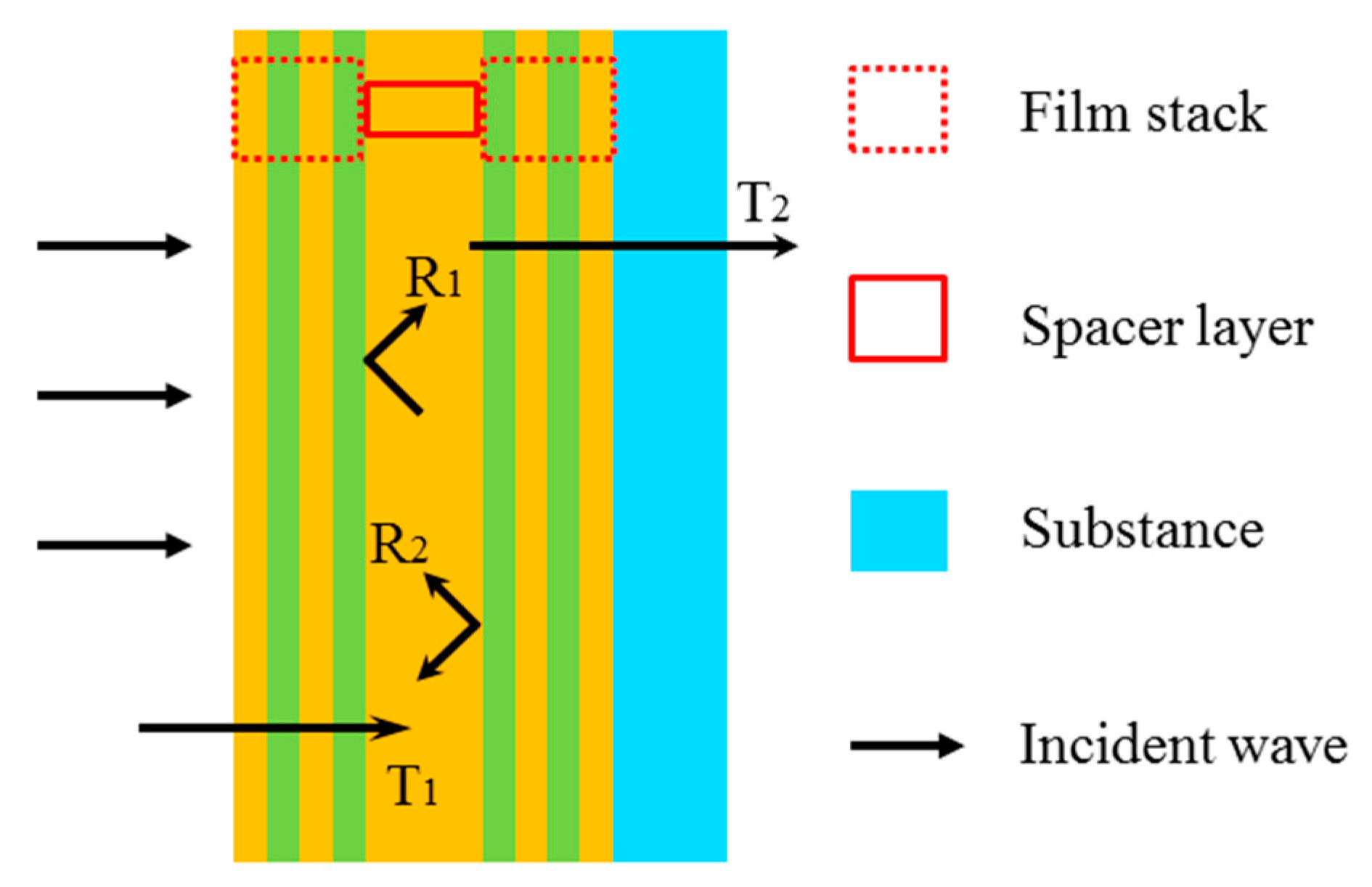
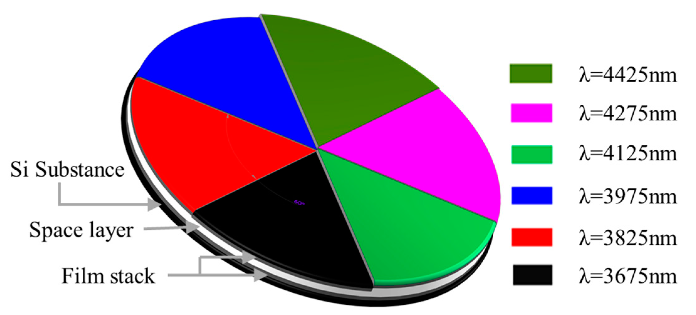
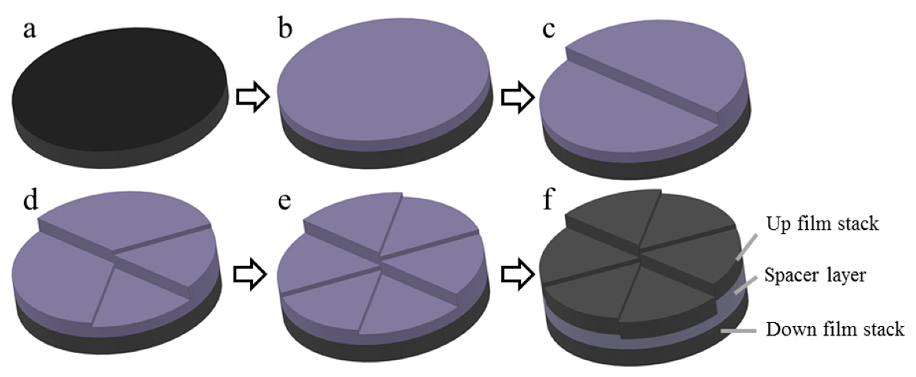
2. Basic Principle and Film Design
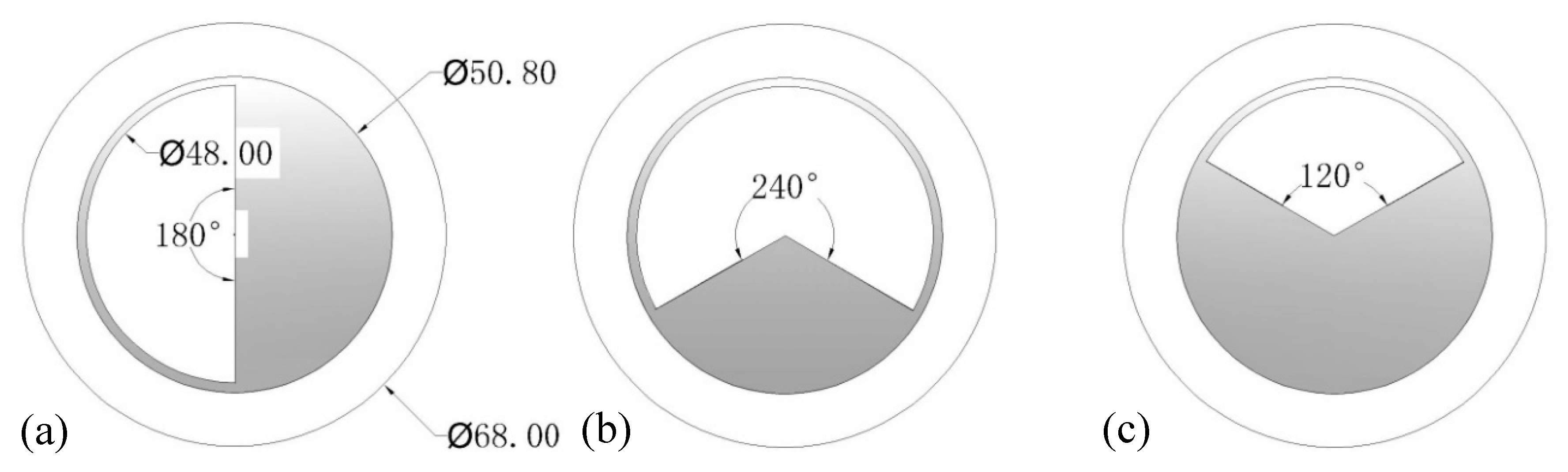
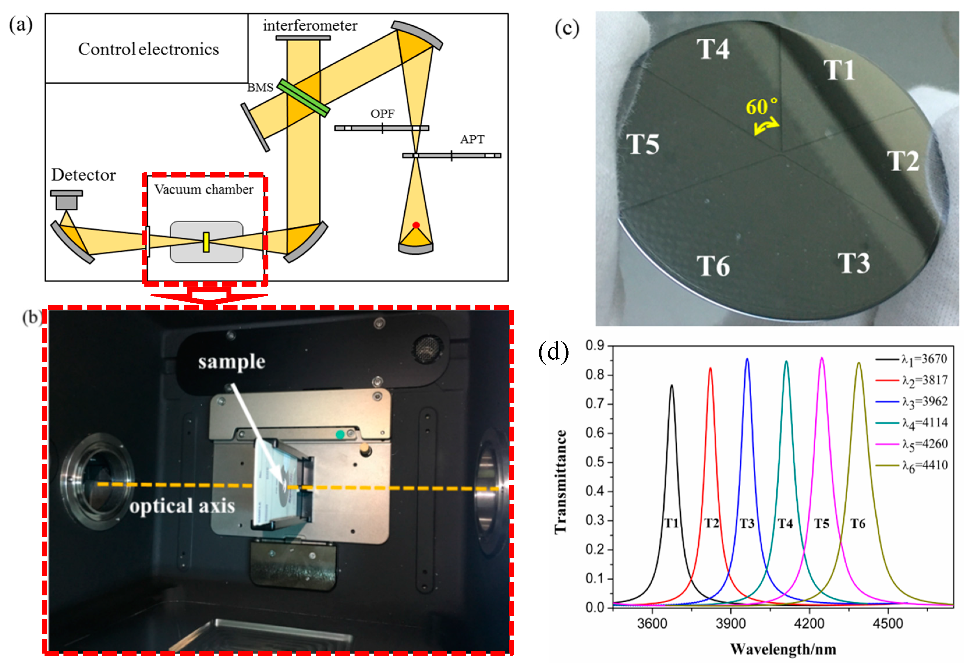
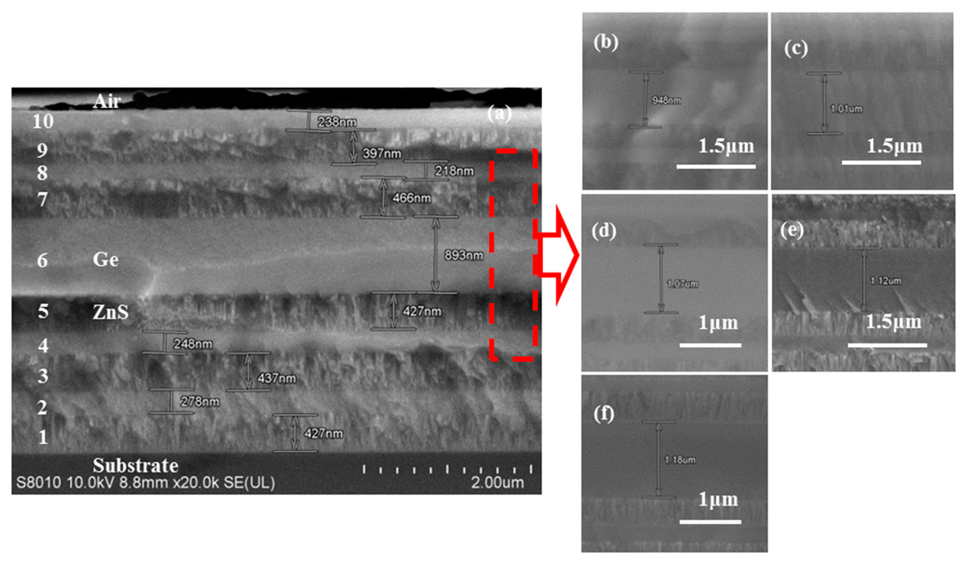
The FP interferometer was composed of a spacer in the middle and two parallel plates outside. The inner surfaces of the plate were coated with the same high-reflectivity film and its reflectivity determined the peak transmittance. The central transmittance wavelength could be selected with a changing thickness of the spacer layer. In an FP narrow-band filter layer system, the plates and spacer could all be substituted by high reflective films and dielectric layers, respectively; its structure is shown in Figure 1.
Transmittance of central wavelength was as following [25]:
T = T 0 / ( 1 + F sin 2 θ )
in Equation (1),
T 0 = T 1 T 2 / ( 1 R 1 R 2 ) 2
F = 4 R 1 R 2 / ( 1 R 1 R 2 ) 2
θ = ( φ 1 + φ 2 2 δ ) / 2
where R1 and R2, T1 and T2 are the reflectance and transmittance of the films stack, respectively; φ1 and φ2 are the reflective phases of the films stack; δ equal to 2πndcosθ/λ, which is the phase thickness of the spacer layer; n is the refractive index of a single layer film; d is the physical thickness of a single layer film and λ is the reference wavelength. R1 and R2, T1 and T2 are all functions of n, d, and λ [25]. Here, we only considered the case of normal incidence of light. The λ0 of the maximum transmittance was determined by Equations (5) and (6).
θ 0 = ( φ 1 + φ 2 4 π λ n d ) / 2 = k π
λ 0 = 2 n d [ k + ( φ 1 + φ 2 ) 2 π ] = 2 n d m
where k is a natural number, m is the order of interference equal to k + (φ1 + φ2)/(2π).
According to the principle mentioned above, six-channel filters working in a wavelength range of 3.5–4.6 μm were designed with reference wavelength of 4 μm, by optimizing the basic film layer structure of G|HLHL aH LHLH|A. Herein, A and G represents air and silicon substrate with indices of 1 and 3.5, respectively. H is Ge materials with a refractive index of 4. L is ZnS materials with a refractive index of 2.17. Their optic thickness are all λ/4. Ge used to be a spacer layer and the coefficient of a was set to modify the thickness of the spacer. Moreover, a suitable matching layer of ZnS was prepared near the substrate to get a high transmittance.
Design films based on the FP theory, the basic layer system, was determined and shown as follows:
G|0.9364L1.087H0.9692L0.9924H0.944L aH 0.6678L1.4277H0.8455L0.9546H|A
The interval between the adjacent center wavelengths was designed to be 150 nm apart, and the corresponding physical thickness difference of the spacer layer was 60 nm. The spectra are shown in Figure 2.
The peak transmittance of each channel could reach 95% or more, and the cutoff transmittance was less than 1%, the full width at half maximum (FWHM) was between 47 and 55 nm. A linear relation between peak wavelength and spacer layer thickness was determined and shown in the inset picture of Figure 1, which obeyed Equation (6).

3. Experiments

The structure of the 6-channels narrow-band filter is shown in Figure 3. Each channel occupied a sector angle of 60° with a center wavelength from 3.675 to 4.425 μm. The three hard masks shown in Figure 4 were designed to realize the 6 channels. Substrate was Si wafer purchased from Zhejiang Lijing Optoelectronics (Hangzhou, China), with a thickness of 0.4 mm and a diameter of 50.8 mm.
First, low reflection films were deposited on silicon substrates and then a 900-nm Ge-film spacer layer was added. Next, two channels, shown in Figure 5c, could be obtained by depositing 180 nm of Ge film with a mask (Figure 4a), and then two 60-nm Ge-film layers were prepared under No. 2 mask and No. 3 mask, respectively. After this, we could get 4 and 6 channels, as shown in Figure 5d,e, respectively. Last, an up-reflective film was prepared, as shown in Figure 5f.
Generally, plating a low refractive index film on a high refractive index substrate is the effective road to increase the transmittance. The ideal single layer antireflection film has an optical thickness of λ/4, and its refractive index needs to satisfy n 1 2 = n 0 × n 2 [25]. Where, n 0 is the refractive index of the incident medium, n 1 is the refractive index of the film and n 2 is the refractive index of the substrate. The refractive index of Y2O3 almost satisfies the above equation, so this film with a λ/4 thickness was deposited on the back surface of the Si substrate. The deposition parameters are shown in Table 1. The deposition rate and thickness were all controlled by using the quartz crystal film thickness controller manufactured by the Shanghai Moringtech Company (Shanghai, China). The gold-plated crystal oscillator was purchased from JJK companies (Albuquerque, NM, USA).

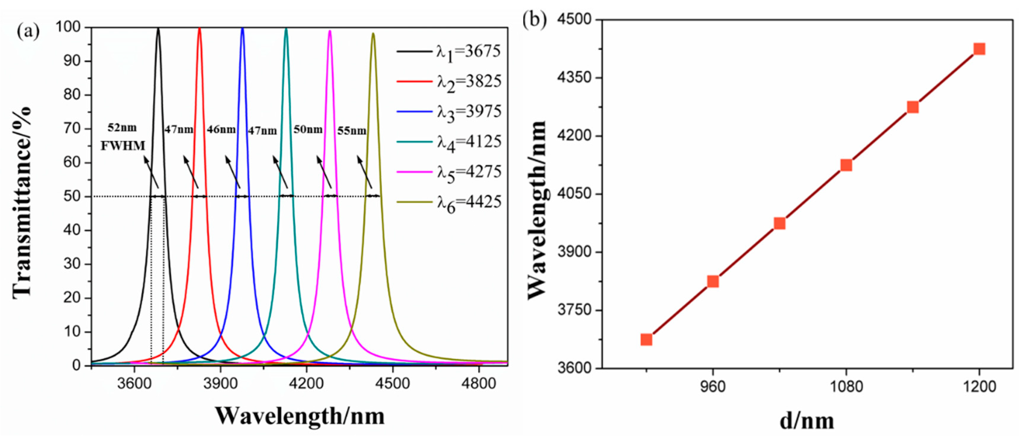
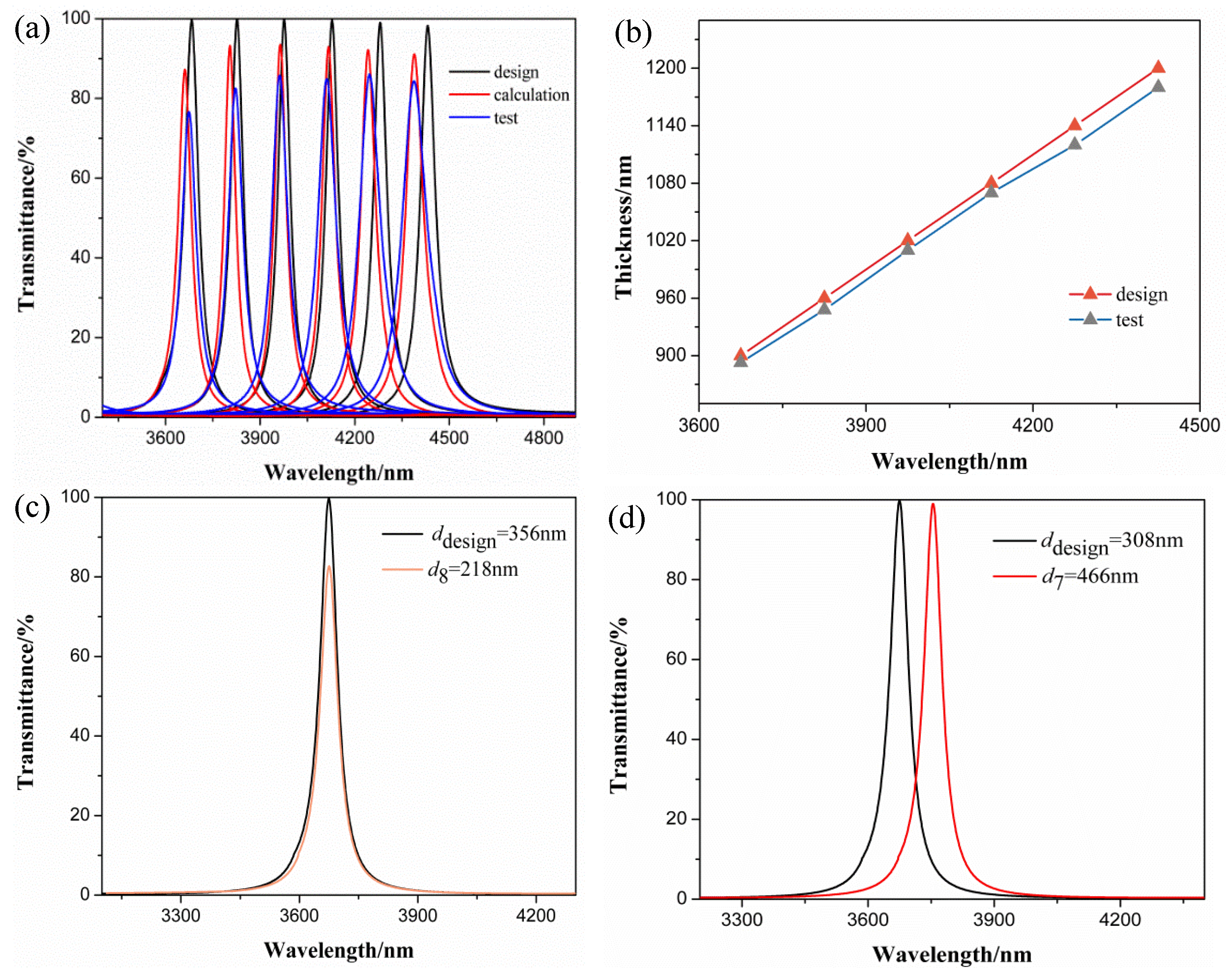
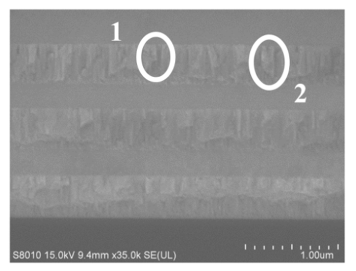
4. Results Discussion and Comparison

Transmission spectra of these samples were all measured by using a vacuum infrared Fourier spectrometer with a type of VERTEX 70V manufactured by BRUKER (Billerica, MA, USA). Its basic measurement optic structure diagram and sample holder are shown in Figure 6a,b, respectively. During measurement, spectral resolution could reach to 2 cm−1, when using an MIR source and each channel was scanned 16 times, to reduce the error. Peak wavelength was determined to a wavelength with maximum spectral transmittance. In order to eliminate the influence of water vapor and other impurities in the air, the measurements were all carried out in a vacuum environment with a pressure less than 0.2 mbar. Incident light with an incident angle near zero and a beam diameter of 2 mm was used to carry out transmittance measurement. The sample and transmittance spectra are shown in Figure 6c,d, respectively.
The channel information is shown in Table 2. The peak wavelength was located in the range of 3.5–4.6 μm, and the peak transmittance varied from 76.5% to 86%. The average FWHM of the six channels was about 50 nm.
The test results showed that the peak transmittance was slightly lower than the design value. Thus, an SEM cross-section of the first channel filter was tested; shown in Figure 7a, and the space layer thickness of channel 2–6 are also show in Figure 7b–f. Details of the thickness difference of each layer are included in Table 3.
According to the results of the tested thickness, the calculated transmittance spectrum of the six channels was acquired; as shown in Figure 8a. The calculated curve Tmax was 14% lower than that of the design, and 5% more than that of test. The peak wavelength position of measurement were determined to be a linear relation, similar to that of the design from Figure 8b. The maximum position difference was about 10 nm and the corresponding relative error was less than 0.35%. Furthermore, we found that the thickness error of layer 7 and 8 showed a giant deviation, as compared to the theory. Therefore, we plotted the transmittance curves with the tested and theoretical thickness of layer 7 and 8, respectively, as shown in Figure 8c,d. It can be observed from Figure 8c that the tested Tmax dropped to 82% with a thickness deviation of 138 nm, but the peak wavelength was maintained here. However, as seen in Figure 8d, the decrease of Tmax was only 3% with a 157 nm thickness deviation, but the displacement of the peak wavelength could be up to 60 nm. Based on the analysis above, it was known that the film thickness deviation was the main cause of the decrease of Tmax and the error of positioning, and each layer played a different role in peak transmittance and wavelength.
Film scatter also caused a decrease in transmittance, and was usually divided into in-body scattering and surface scattering [26,27]. In-body scattering was due to the difference in refractive index caused by the columnar structure (circle 2) and gap (circle 1) of the evaporated film, as shown in Figure 9.
Table 4 shows a comparison of the commercial products [28,29,30] and our filter. Most of the products were single-channel narrow-band filters, and the peak position deviation was between ±15 and ±20 nm. However, the peak position deviation in this work was between ±5 and ±15 nm, and the peak position error (Δλ/λ0, Δλ, and λ0 were the positioning accuracy and peak wavelength, respectively) was controlled within 0.13%–0.35%, which were far less than the same type of products in the market. In this work, the average peak transmittance could go up to 83%, which was greater than the others.

5. Conclusions

In our work, a 6-channel narrow-band filter with higher optical properties was developed on the basis of the FP theory, using three hard masks, to modify spacer thickness. The average peak transmittance was more than 83%, the cutoff transmittance was less than 1%, peak positioning accuracy error was less than 0.35% and a passband half-width varying from 55 to 94 nm, were observed. These properties are better than that of a commercial filter. In the test results section, a single factor analysis showed that the deviation of Ge and ZnS film thickness was the main reason for the decrease in Tmax and the location error, respectively. The combination of the two factors would greatly reduce the peak transmittance and the location accuracy of the central wavelength.

Author Contributions

Conceptualization, H.L.; Methodology, H.L. and Y.D.; software, Y.D.; Validation, Y.D., C.C., T.J. and S.Y.; Writing—original draft preparation, Y.D.; Writing—review and editing, H.L.

Funding

This research was funded by Community Technology (41423060201); Xi’an Key Laboratory of Intelligent Detection and Perception (201805061ZD12CG45); Research Project of Key Laboratory of Shaanxi Provincial Department of Education (17JS049); Key Industry Innovation Chain Project of Shaanxi Provincial Science and the Technology Department (2018ZDCXL-GY-08-02-01).

Acknowledgments

We are grateful to Haifeng Liang and Changlong Cai for their guidance and assistance throughout the process, and thanks to the Key Laboratory of Optical Measurement and Thin Film of Shaanxi Province for providing platform support.

Conflicts of Interest

The authors declare no conflict of interest.

References

  1. Yang, G.P.; Yu, X.C.; Feng, W.F.; Liu, W.; Chen, W. The development and application of hyperspectral RS technology. Bull. Surv. Mapp. 2018, 10, 1–4. [Google Scholar]
  2. Yang, Y.Z.; Cao, W.X.; Sun, Z.H.; Wang, G.F. Development of real-time hyperspectral radiation sea-observation system. Acta Opt. Sin. 2009, 29, 102–107. [Google Scholar] [CrossRef]
  3. Wen, Z.Y.; Chen, G.; Wang, J.G. The project and simulation of a compositive miniature spectrum instrument based on the array of Fabry-Perot cavity. Spectrosc. Spectr. Anal. 2006, 26, 1955–1959. [Google Scholar]
  4. Lei, Y.; Ming-ming, X.; Jie-xiang, C.; Hui, X. Optical system of the hyper-spectral imager for the underwater environment and targets monitoring. Acta Photonica Sin. 2018, 47, 3071. [Google Scholar]
  5. Cao, H.Y.; Gao, H.T.; Zhao, C.G. Development of china land quantitative remote sensing satellite technology. Spacecr. Eng. 2018, 27, 1673–8748. [Google Scholar]
  6. Dai, L.Q.; Tang, S.F.; Xu, L.N.; Sun, Q.Y.; Yang, X.B.; Wang, Z.M.; Jin, Z.T.; Zhao, Y.H. Development overview of space-borne mulita-spectral imager band range from visible to thermal infrared. Infrared Technol. 2019, 41, 1001–8891. [Google Scholar]
  7. Ju, H.; Wu, Y.H. The miniaturization of spectrometers. Chin. J. Sci. Instrum. 2001, S2, 131–133. [Google Scholar]
  8. Zhou, Y.; Yang, H.H.; Liu, Y.; Lin, S. Application and development of hyperspectral imaging technology. J. Astronaut. Metrol. Meas. 2017, 37, 1000–7202. [Google Scholar]
  9. Cai, Y.; Liu, D.Q.; Luo, H.H. Design and fabrication of 3.5~4.0 μm band-pass filter working at cryogenic temperature. Chin. J. Lasers 2012, 39, 1101003. [Google Scholar]
  10. Edmund Optics Worldwide. Bandpass Filters. Available online: http://www.edmundoptics.com/f/infrared-ir-bandpass-filters/14290/ (accessed on 4 September 2019).
  11. Seoul Precision Opics Co. Infrared Band Pass Filter. Available online: http://www.spocc.com/infrared-filter.html (accessed on 4 September 2019).
  12. Northumbria Optical Coatings. Narrow Band Pass Filters. Available online: http:// https://www.noc-ltd.com/catalogue (accessed on 4 September 2019).
  13. Semrock. Band Pass Filters. Available online: http://www.nmerry.com/lvguangpian/Semrock/2016/0906/355.html (accessed on 4 September 2019).
  14. Bright, C.I. Electrically conductive and infrared transparent thin metal film coatings. SPIE Opt. Eng. 1986, 678, 202–210. [Google Scholar]
  15. Jan, K.; Sven, P.; Bernd, G. Mid-infrared optical properties of thin films of aluminum oxide, titanium dioxide, silicon dioxide, aluminum nitride, and silicon nitride. Appl. Opt. 2012, 51, 6789–6798. [Google Scholar]
  16. Wang, Z.S.; Wang, L.; Sang, T.; Wu, Y.G.; Jiao, H.F.; Zhu, J.T.; Chen, L.Y.; Wang, S.W.; Chen, X.S.; Lu, W. Design and fabrication of narrow band multichannel filters. Infrared Laser Eng. 2007, 36, 1007–2267. [Google Scholar]
  17. Wang, S.W.; Wang, L.; Wu, Y.G.; Wang, Z.S.; Liu, D.Q.; Lin, B.; Chen, X.S.; Lu, W. Arrays of narrow bandpass filters fabricated by combinatorial etching technique. Infrared Laser Eng. 2006, 26, 746–751. [Google Scholar]
  18. Luo, H.H.; Li, Y.P.; Cai, Q.Y.; Liu, D.Q. Fabrication of 8-channel micro integrated filter in 2.0~2.4μm by combine masks and plating. Chin. J. Lasers 2012, 39, 1107001. [Google Scholar]
  19. Fang, C.L.; Dai, B.; Qiao, X.; Wang, Q.; Zhang, D.W. Optoflui dictunable linear narrow-band filter based on braggnanocavity. Photonics J. 2016, 9, 1–8. [Google Scholar]
  20. Tang, H.L.; Gao, J.S.; Zhang, J.; Wang, X.Y.; Fu, X.H. Preparation and spectrum characterization of a high quality linear variable filter. Coatings 2018, 8, 308. [Google Scholar] [CrossRef]
  21. Lin, B.; Liu, D.Q.; Kong, L.F.; Zhang, F.S. Fabrication of mid-infrared 8-channel micro integrated filter. Acta Photonica Sin. 2005, 34, 1316–1319. [Google Scholar]
  22. Zhang, L.; Ni, R.; Huang, C.; Li, B.; Liu, D.Q. Fabrication of a narrow bandpass optical filter with center wavelength at 14.95 μm. Acta Photonica Sin. 2014, 34, 731003. [Google Scholar]
  23. Chen, P.; Luo, L.W.; Sheng, B.; Huang, Y.S. Study on fabrication method of linear variable filter. Opt. Instrum. 2016, 4, 308. [Google Scholar]
  24. Chen, C.P.; Shi, J.T.; Guo, R.; Bai, B.; Yang, C.M.; Guo, H.X. Design and preparation of Min-infrared bandpass filter. J. Appl. Opt. 2012, 33, 595–598. [Google Scholar]
  25. Tang, J.F.; Gu, P.F.; Liu, X.; Li, H.F. Modern Optical Thin Film Technology, 1th ed.; Zhejiang University Press: Hang Zhou, China, 2006. [Google Scholar]
  26. Guenther, K.H.; Gruber, H.L. Morphology and light scattering of dielectric multilayer systems. Thin Solid Film. 1979, 34, 343. [Google Scholar] [CrossRef]
  27. Lu, J.J.; Liu, W.G.; Pan, Y.Q. Optical Thin Film Technology, 2th ed.; Publishing House of Electronics Industry: Beijing, China, 2011. [Google Scholar]
  28. Spectrogon. Narrow-Band Filters. Available online: http://www.nmerry.com/lvguangpian/Spectrogon/2016/0906/341.html (accessed on 4 September 2019).
  29. HB-Optical. Near-Infrared Band-Pass Filters. Available online: http://www.hb-optical.com/products_detail/productId =104.html (accessed on 4 September 2019).
  30. Alluxa. Ultra Narrow Band-Pass Filters. Available online: http://www.nmerry.com/lvguangpian/Alluxa/2018/0622/514.html (accessed on 4 September 2019).
Figure 1. Fabray–Perot (FP) film structure.
Coatings 09 00567 g001
Figure 2. (a) Transmittance spectra of a 6-channel fan-shaped integrated narrow-band filter; (b) the relationship between the peak wavelength position and the physical thickness of the spacer layer.
Coatings 09 00567 g002
Figure 3. The 6-channel fan-shaped integrated narrow-band filters structure.
Coatings 09 00567 g003
Figure 4. Mask for plating the spacer layer, (a) No. 1 mask; (b) No. 2 mask; (c) No. 3 mask.
Coatings 09 00567 g004
Figure 5. Schematic diagram of the spacer-layer deposition process of a 6-channel sector integrated narrowband filter. (a) Down film stack; (b) a 900-nm Ge-film was added on (a); (c) Add 180nm Ge film on (b) using mask No. 1; (d) Add 60 nm Ge film on (c) using mask No. 2; (e) Add 60 nm Ge film on (d) using mask No. 3; (f) a up film stack was added on (e).
Coatings 09 00567 g005
Figure 6. (a) Test equipment structure diagram; (b) sample holder; (c) fan-shaped integrated narrow-band filter test sample; and (d) transmittance spectra.
Coatings 09 00567 g006
Figure 7. (a) SEM test chart of the first channel filter sample; (bf) is a sectional view of the second to sixth channel spacer layer.
Coatings 09 00567 g007
Figure 8. (a) Thickness calculated spectra, design spectra and test spectra comparison chart; (b) Tmax position theory and test comparison chart; (c) a spectra of the influence of the thickness of the eighth layer Ge on the transmittance; (d) a spectra of the influence of the thickness of the seventh layer ZnS on the transmittance.
Coatings 09 00567 g008
Figure 9. ZnS-film microstructure.
Coatings 09 00567 g009
Table 1. Material deposition parameters.
MaterialBase Pressure Vacuum (Pa)Temperature (°C)Evaporation Rate (nm/s)
Ge1.3 × 10−31200.3
ZnS3 × 10−31050.4
Y2O32 × 10−32500.4
Table 2. The 6-channel information.
ChannelT1T2T3T4T5T6
Peak position (nm)367038173962411442604410
Transmittance (%)76.582.585.784.886.784.3
FWHM (nm)55.9855.6460.2769.379.6493.53
Table 3. Theoretical thickness and test thickness difference table.
Film NumberDesign Thickness (nm)Test Thickness (nm)Deviation (nm)
1432.04427−5.04
2271.75278−6.25
3447.1543710.15
4248.112480.11
5435.544278.54
69008937
96094812
1020101010
1080107010
1140112020
1200118020
7308.11466−157.89
8356218138
9390.06397−6.94
10238.652380.65
Table 4. Optical properties comparison table.
Company NamePeak Wavelength (nm)Base MaterialFilter Channel CharacteristicsPositioning Accuracy (nm)Peak Transmittance
Spectrogon3700SiliconSingle-channel±2075%
3860SapphireSingle-channel±2060%
4120SapphireSingle-channel±2070%
4270SapphireSingle-channel±2570%
4275SapphireSingle-channel±1570%
4515SapphireSingle-channel±2070%
HB-Optical2100Single-channel±1075%
2200Single-channel±1075%
Alluxa1064SiliconSingle-channel85%
In this work3675Silicon6 channels integration±1076.5%
3825±1082.5%
3975±1085.7%
4125±1084.8%
4275±1086%
4425±1084.3%

