Structure of Highly Porous Silicon Dioxide Thin Film: Results of Atomistic Simulation

Abstract
:
1. Introduction
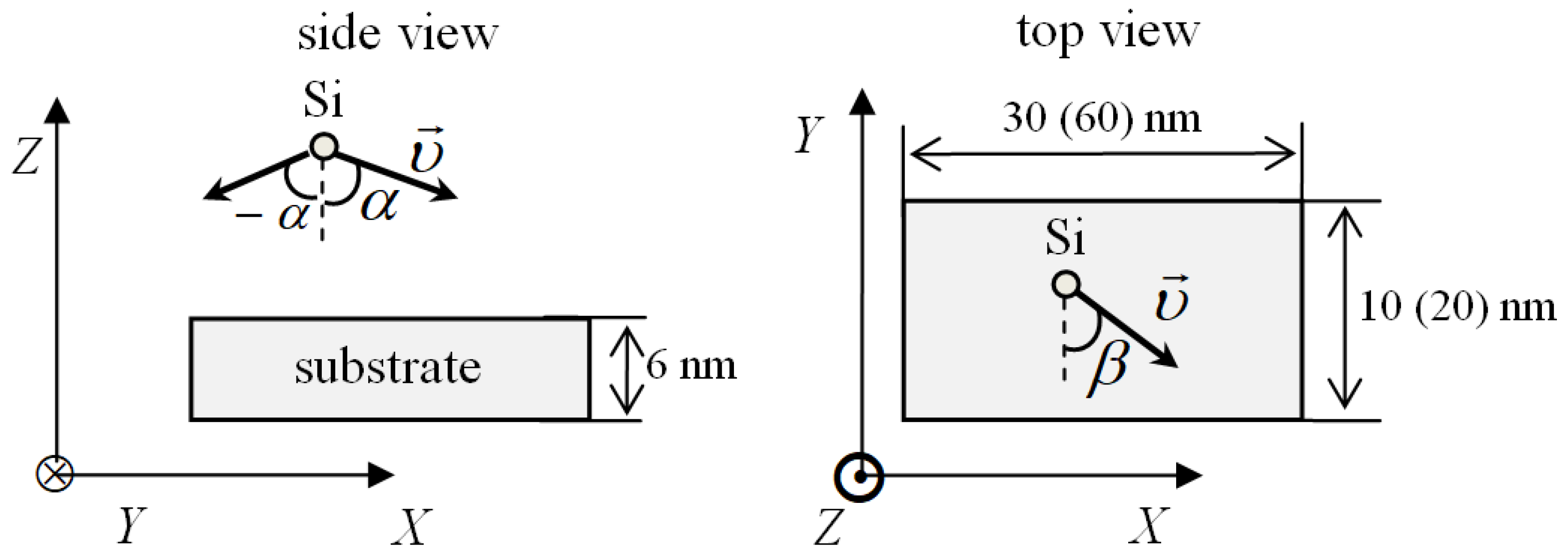
2. Method
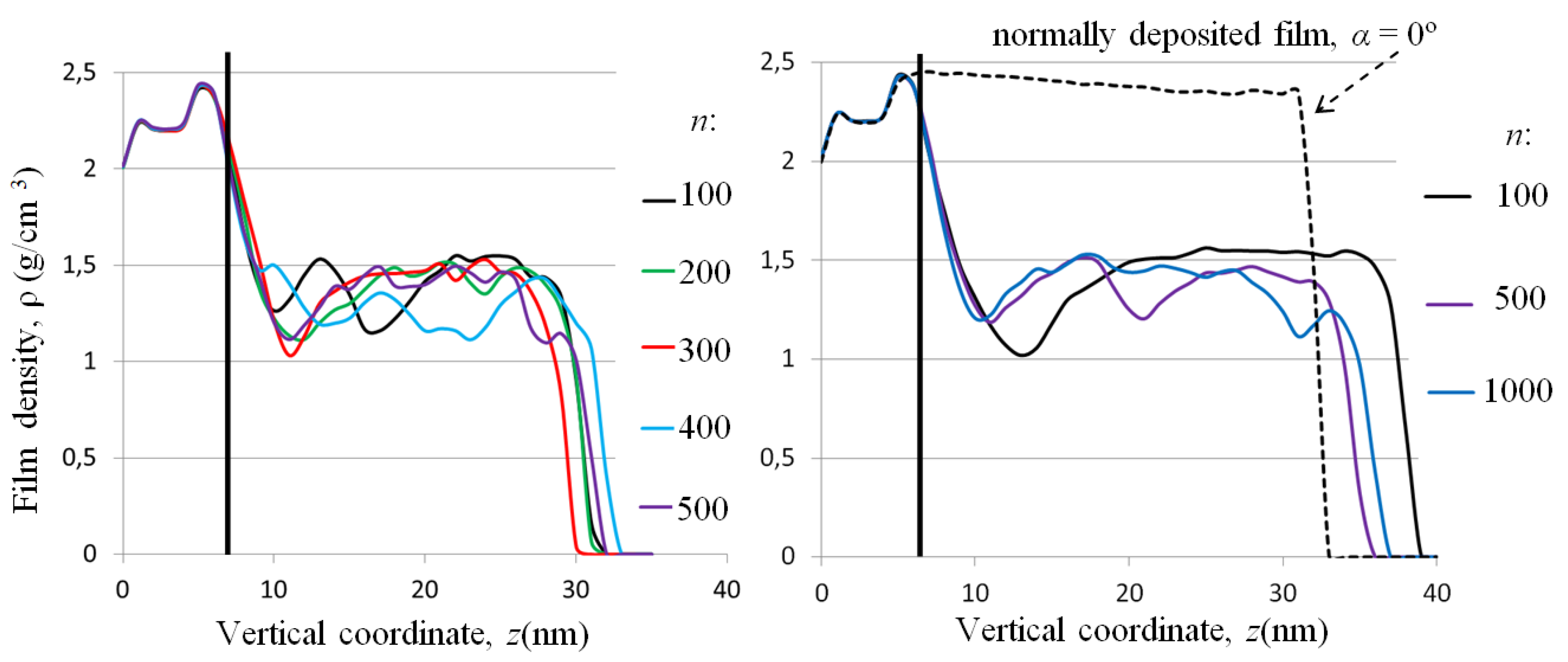
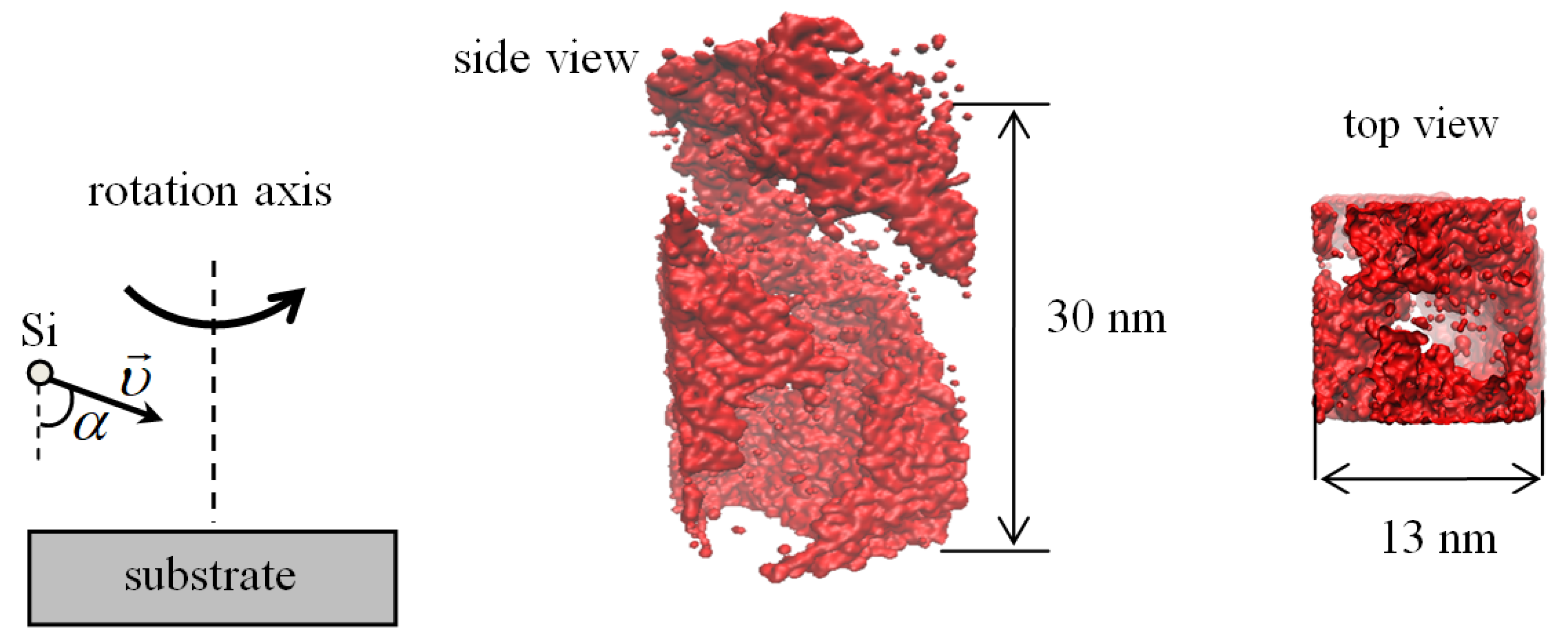
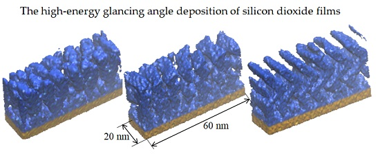
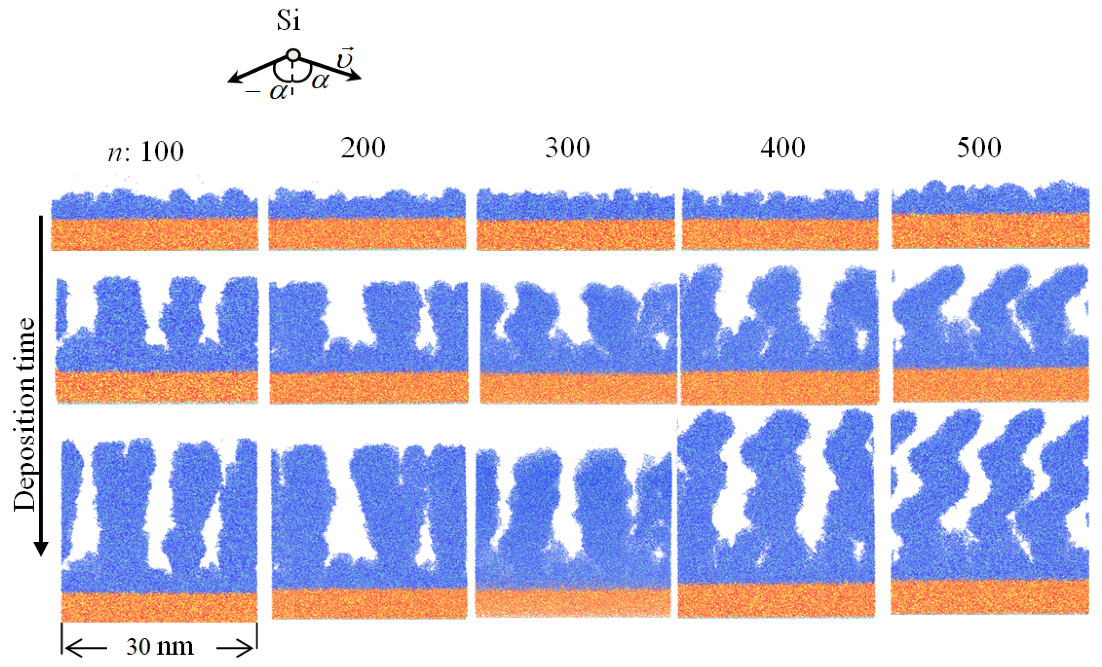
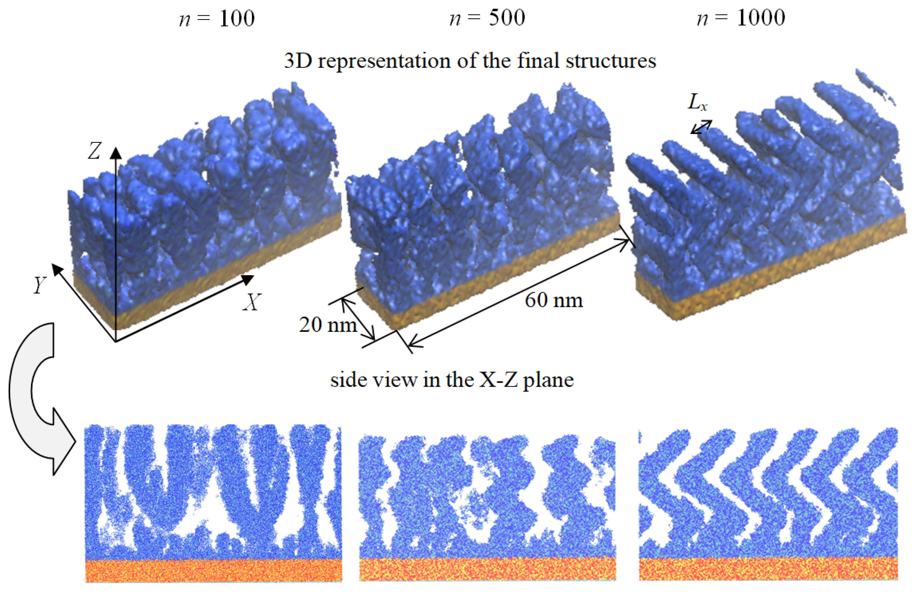
3. Results and Discussion
4. Conclusions
Author Contributions
Funding
Conflicts of Interest
References
- Robbie, K.; Brett, M.J.; Lakhtakia, A. Chiral sculptured thin films. Nature 1996, 384, 616. [Google Scholar] [CrossRef]
- Hawkeye, M.M.; Brett, M.J. Glancing angle deposition: fabrication, properties, and applications of micro- and nanostructured thin films. J. Vac. Sci. Technol. 2007, 25, 1317–1335. [Google Scholar] [CrossRef]
- Woo, S.-H.; Park, Y.J.; Chang, D.H.; Sobahan, K.M.A.; Hwangbo, C.K. Wideband antireflection coatings of porous MgF2 films by using glancing angle deposition. J. Korean Phys. Soc. 2007, 51, 1501–1506. [Google Scholar] [CrossRef]
- Tkachenko, V.; Marino, A.; Otón, E.; Bennis, N.; Otón, J.M. Morphology of SiO2 films as a key factor in alignment of liquid crystals with negative dielectric anisotropy. Beilstein J. Nanotechnol. 2016, 7, 1743–1748. [Google Scholar] [CrossRef]
- Trottier-Lapointe, W.; Zabeida, O.; Schmitt, T.; Martinu, L. Ultralow refractive index optical films with enhanced mechanical performance obtained by hybrid glancing angle deposition. Appl. Opt. 2016, 55, 8796–8805. [Google Scholar] [CrossRef]
- Tolenis, T.; Grinevičiūtė, L.; Buzelis, R.; Smalakys, L.; Pupka, E.; Melnikas, S.; Selskis, A.; Drazdys, R.; Melninkaitis, A. Sculptured anti-reflection coatings for high power lasers. Opt. Mater. Express 2017, 7, 1249–1258. [Google Scholar] [CrossRef]
- Oliver, J.B.; Kessler, T.J.; Smith, C.; Taylor, B.; Gruschow, V.; Hettrick, J.; Charles, B. Electron-beam–deposited distributed polarization rotator for high-power laser applications. Opt. Express 2014, 22, 23883–23896. [Google Scholar] [CrossRef]
- Oliver, J.B.; Smith, C.; Spaulding, J.; Rigatti, A.L.; Charles, B.; Papernov, S.; Taylor, B.; Foster, J.; Carr, C.W.; Luthi, R.; et al. Glancing-angle–deposited magnesium oxide films for high-fluence applications. Opt. Mat. Express 2016, 6, 2291–2303. [Google Scholar] [CrossRef]
- Karabacak, T.; Singh, J.P.; Zhao, Y.P.; Wang, G.C.; Lu, T.M. Scaling during shadowing growth of isolated nanocolumns. Phys. Rev. B 2003, 68, 125408. [Google Scholar] [CrossRef] [Green Version]
- Robbie, K.; Brett, M.J.; Lakhtakia, A. First thin-film realization of a helicoidal bianisotropic medium. J. Vac. Sci. Technol. A 1995, 13, 2991–2993. [Google Scholar] [CrossRef]
- Smy, T.; Vick, D.; Brett, M.J.; Dew, S.K.; Wu, A.T.; Sit, J.C.; Harris, K.D. Three-dimensional simulation of film microstructure produced by glancing angle deposition. J. Vac. Sci. Technol. A 2000, 18, 2507–2512. [Google Scholar] [CrossRef]
- Grüner, C.; Liedtke, S.; Bauer, J.; Mayr, S.G.; Rauschenbach, B. Morphology of Thin Films Formed by Oblique Physical Vapor Deposition. ACS Appl. Nano Mat. 2018, 1, 1370–1376. [Google Scholar] [CrossRef]
- Backholm, M.; Foss, M.; Nordlund, K. Roughness of glancing angle deposited titanium thin films: an experimental and computational study. Nanotechnology 2012, 23, 385708. [Google Scholar] [CrossRef] [Green Version]
- Badorreck, H.; Steinecke, M.; Jensen, L.; Ristau, D.; Jupé, M.; Müller, J.; Tonneau, R.; Moskovkin, P.; Lucas, S.; Pflug, A.; et al. Correlation of structural and optical properties using virtual materials analysis. Opt. Express 2019, 27, 22209–22225. [Google Scholar] [CrossRef]
- Schmidt, D.; Schubert, M. Anisotropic bruggeman effective medium approaches for slanted columnar thin films. J. Appl. Phys. 2013, 114, 083510. [Google Scholar] [CrossRef]
- Grigoriev, F.V.; Sulimov, A.V.; Katkova, E.V.; Kochikov, I.V.; Kondakova, O.A.; Sulimov, V.B.; Tikhonravov, A.V. computational experiments on atomistic modeling of thin film deposition. Appl. Opt. 2017, 56, C87–C90. [Google Scholar] [CrossRef]
- Grigoriev, F.V.; Sulimov, A.V.; Katkova, E.V.; Kochikov, I.V.; Kondakova, O.A.; Sulimov, V.B.; Tikhonravov, A.V. Full-atomistic nanoscale modeling of the ion beam sputtering deposition of SiO2 thin films. J. N. Cryst. Sol. 2016, 448, 1–5. [Google Scholar] [CrossRef]
- Grigoriev, F.V.; Sulimov, A.V.; Katkova, E.V.; Kochikov, I.V.; Kondakova, O.A.; Sulimov, V.B.; Tikhonravov, A.V. Annealing of deposited SiO2 thin films: full-atomistic simulation results. Opt. Mat. Express 2016, 6, 3960–3966. [Google Scholar] [CrossRef]
- Grigoriev, F.V.; Sulimov, V.B.; Tikhonravov, A.V. Atomistic simulation of the glancing angle deposition of SiO2 thin films. J. N. Cryst. Sol. 2019, 512, 98–102. [Google Scholar] [CrossRef]
- Grigoriev, F.V.; Sulimov, A.V.; Kochikov, I.V.; Kondakova, O.A.; Sulimov, V.B.; Tikhonravov, A.V. Supercomputer modeling of the ion beam sputtering process: full-atomistic level. In Proceedings of the SPIE—The International Society for Optical Engineering, Jena, Germany, 21–24 September 2015; Volume 9627, pp. 962708-1–962708-9. [Google Scholar] [CrossRef]
- Thompson, M.V. Atomic collision cascades in solids. Vacuum 2002, 66, 99–114. [Google Scholar] [CrossRef]
- Berendsen, H.J.C.; Postma, J.P.M.; van Gunsteren, W.F.; DiNola, A.; Haak, J.R. Molecular-dynamics with coupling to an external bath. J. Chem. Phys. 1984, 81, 3684–3690. [Google Scholar] [CrossRef]
- Abraham, M.J.; Murtola, T.; Schulz, R.; Páll, S.; Smith, J.C.; Hess, B.; Lindahl, E. GROMACS: High performance molecular simulations through multi-level parallelism from laptops to supercomputers. SoftwareX 2015, 1–2, 19–25. [Google Scholar] [CrossRef]
- Humphrey, W.; Dalke, A.; Schulten, K. VMD: Visual molecular dynamics. J. Mol. Graph. 1996, 14, 33–38. [Google Scholar] [CrossRef]
- Voevodin, V.l.; Antonov, A.; Nikitenko, D.; Shvets, P.; Sobolev, S.; Sidorov, I.; Stefanov, K.; Voevodin, V.V.; Zhumatiy, S. Supercomputer lomonosov-2: large scale, deep monitoring and fine analytics for the user community. Supercomput. Front. Innov. 2019, 6, 4–11. [Google Scholar] [CrossRef]
- Lakhtakia, A.; Mesier, R. Sculpured thin Films: Nanoengineered Morphology and Optics; SPIE: Bellingham, WA, USA, 2005. [Google Scholar]
- Christian, P.; Glancing Angle Deposition of Silicon Nanostructures by on Beam Sputtering. Universität Leipzig, Dissertation. Available online: https://www.iom-leipzig.de/fileadmin/redaktion/pdf/Dissertationen/Diss_Patzig_200dpi_sicher.pdf (accessed on 5 August 2019).
- Vedam, K.; Limsuwan, P. Piezo- and elasto-optic properties of liquids under high pressure. II. Refractive index vs. density. J. Chem. Phys. 1978, 69, 4772–4778. [Google Scholar] [CrossRef]
- Melninkaitis, A.; Grinevičiūtė, L.; Abromavičius, G.; Mažulė, L.; Smalakys, L.; Pupka, E.; Ščiuka, M.; Buzelis, R.; Kičas, S.; Tolenis, T. Next-generation allsilica coatings for UV applications. In Proceedings of the SPIE 10447, Laser-Induced Damage in Optical Materials, Boulder, CO, USA, 24–27 September 2017. 104470U. [Google Scholar] [CrossRef]


| Subst. Dimens. | 10 nm × 30 nm | 20 nm × 60 nm | ||||||
|---|---|---|---|---|---|---|---|---|
| n | 100 | 200 | 300 | 400 | 500 | 100 | 500 | 1000 |
| ρ | 1.31 | 1.34 | 1.39 | 1.26 | 1.44 | 1.33 | 1.32 | 1.35 |
© 2019 by the authors. Licensee MDPI, Basel, Switzerland. This article is an open access article distributed under the terms and conditions of the Creative Commons Attribution (CC BY) license (http://creativecommons.org/licenses/by/4.0/).
Share and Cite
Grigoriev, F.V.; Sulimov, V.B.; Tikhonravov, A.V. Structure of Highly Porous Silicon Dioxide Thin Film: Results of Atomistic Simulation. Coatings 2019, 9, 568. https://doi.org/10.3390/coatings9090568
Grigoriev FV, Sulimov VB, Tikhonravov AV. Structure of Highly Porous Silicon Dioxide Thin Film: Results of Atomistic Simulation. Coatings. 2019; 9(9):568. https://doi.org/10.3390/coatings9090568
Chicago/Turabian StyleGrigoriev, F.V., V.B. Sulimov, and A.V. Tikhonravov. 2019. "Structure of Highly Porous Silicon Dioxide Thin Film: Results of Atomistic Simulation" Coatings 9, no. 9: 568. https://doi.org/10.3390/coatings9090568
APA StyleGrigoriev, F. V., Sulimov, V. B., & Tikhonravov, A. V. (2019). Structure of Highly Porous Silicon Dioxide Thin Film: Results of Atomistic Simulation. Coatings, 9(9), 568. https://doi.org/10.3390/coatings9090568