Article

Vacuum-Free and Highly Dense Nanoparticle Based Low-Band-Gap CuInSe2 Thin-Films Manufactured by Face-to-Face Annealing with Application of Uniaxial Mechanical Pressure

Materials Department 6 (i-meet), Friedrich-Alexander-University Erlangen-Nürnberg (FAU), Martensstr. 7, 91058 Erlangen, Germany
*
Author to whom correspondence should be addressed.
Coatings 2019, 9(8), 484; https://doi.org/10.3390/coatings9080484
Submission received: 13 May 2019 / Revised: 17 July 2019 / Accepted: 29 July 2019 / Published: 31 July 2019

Abstract

:
Copper indium gallium sulfo-selenide (CIGS) based solar cells show the highest conversion efficiencies among all thin-film photovoltaic competition. However, the absorber material manufacturing is in most cases dependent on vacuum-technology like sputtering and evaporation, and the use of toxic and environmentally harmful substances like H2Se. In this work, the goal to fabricate dense, coarse grained CuInSe2 (CISe) thin-films with vacuum-free processing based on nanoparticle (NP) precursors was achieved. Bimetallic copper-indium, elemental selenium and binary selenide (Cu2−xSe and In2Se3) NPs were synthesized by wet-chemical methods and dispersed in nontoxic solvents. Layer-stacks from these inks were printed on molybdenum coated float-glass-substrates via doctor-blading. During the temperature treatment, a face-to-face technique and mechanically applied pressure were used to transform the precursor-stacks into dense CuInSe2 films. By combining liquid phase sintering and pressure sintering, and using a seeding layer later on, issues like high porosity, oxidation, or selenium- and indium-depletion were overcome. There was no need for external Se atmosphere or H2Se gas, as all of the Se was directly in the precursor and could not leave the face-to-face sandwich. All thin-films were characterized with scanning electron microscopy (SEM), energy dispersive X-ray spectroscopy (EDX), X-ray diffraction (XRD), and UV/vis spectroscopy. Dense CISe layers with a thickness of about 2–3 µm and low band gap energies of 0.93–0.97 eV were formed in this work, which show potential to be used as a solar cell absorber.

1. Introduction

Solar cells from copper indium gallium sulfo-selenide (CIGS) reach a certified efficiency of 23.35% [1] when manufactured in batches and by processes using vacuum technology like sputtering or evaporation and toxic substances like H2Se or at least maintaining a Se atmosphere during annealing. Vacuum-free processing and improving the scalability of absorber fabrication would be very beneficial. CIGS nanoparticles (NPs) have successfully been used recently to achieve dense absorber layers [2,3] and high-efficiency solar cells, with, for example, 13.8% [4] or 15% [5] efficiency. An alcohol-based molecular precursor yielded 14.4% efficiency [6] while using H2Se annealing. Ink-jet printing of CIGS nanoparticles [7] or molecular precursors [8,9], which sometimes uses hydrazine as solvent, shows the possibility of low-cost solar cell absorbers with precise deposition techniques. Even an all solution processed CIGS device with an efficiency of 13.8% was fabricated while using H2Se annealing [10].
However, the CISe, without gallium and sulfur in the system, despite the usually lower efficiency than CIGS, also has its own interesting applications. For example, a CuInSe2 (CISe) thin-film solar cell with a low band-gap of only 0.95 eV has been demonstrated and successfully used as a bottom cell in a tandem solar cell approach [11]. Moreover, it is a less complex system compared with CIGS, thus making it a good material to develop new manufacturing processes and study certain effects, always with the prospect to also apply the process in CIGS production.
In this work, the vacuum-free manufacturing of a CuInSe2 (CISe) thin-film is described. Nanoparticle-based inks with environmentally non-harmful dispersants were thus deposited by low-cost and easily up-scalable doctor-blading. The synthesized nanoparticle precursors were bimetallic Cu-In and elemental Se, as well as the binary selenides Cu2−xSe and In2Se3, dispersed in isopropanol as nano-inks. Moreover, a face-to-face annealing technique was used, which applies mechanical pressure to the sample during the annealing process. Therefore, a combination of liquid phase sintering and pressure sintering with the chemical reaction sintering during the CISe formation can be achieved, which uses particle rearrangement, capillary forces, and creeping to densify the nanoparticle-film. The resulting 2–3 µm dense CISe layers show a low band gap energy of 0.93–0.97 eV, which are described to have promising prospects for use as an absorber layer [11] when the surface smoothness is improved. In the future, a continuous nano-ink deposition on infinite substrates and a temperature treatment using roll-to-roll machines might be used for CIGS absorber fabrication.

2. Materials and Methods

An overview of the experimental processes listing the used nanoparticles and visualizing the face-to-face method is shown in Figure 1.

2.1. Synthesis of Nanoparticles

All chemicals mentioned below were used as received without further purification and the syntheses were performed in ambient conditions if not described otherwise.
Cu-In NP: Bimetallic, slightly indium-rich copper-indium nanoparticles were synthesized according to the works of [12,13,14]. CuCl2 (1 mmol) and InCl3 (1.12 mmol) were dissolved in 150 °C hot tetra ethylene glycol (TEG), while a reducing agent solution was prepared separately by dissolving NaBH4 (14.84 mmol) in 10 °C pre-cooled TEG. Both solutions were then dropped together in a third beaker at room temperature under vigorous stirring using a Reglo Digital MS-4 peristaltic pump (Ismatec, Wertheim, Germany) and immediately formed a black precipitate. To terminate the bubbling alcoholysis and remove excess BH4, acetone was added to the beaker 10 min after the reaction was finished. The copper-poor indium-rich nanoparticles with a Cu/In ratio of 0.89 were isolated by centrifugation, washed several times with isopropanol (IPA), and finally dispersed in IPA.
Se NP: Elemental selenium nanoparticles were synthesized according to the works of [15,16,17]. The Se NPs were fabricated from a 0.127 mol/L Na2SeSO3 solution, prepared by dissolving Na2SO3 and Se powder in 80 °C hot deionized (DI) water after aging for more than 24 h. To stabilize the nanoparticles, a 1.35 mmol/L polyvinylpyrrolidone (PVP) solution was used containing trisodium citrate (2.38 mmol) as acidic buffer. Then, 25 mL of the Na2SeSO3 precursor solution was mixed into the stabilizing solution and 15 mL HCl was added at room temperature. The solution immediately turned from clear to an orange-red murky color. After 1 h of stirring, the nanoparticles were isolated by centrifugation and washed several times with pre-cooled deionized water. For storage, the particles were concentrated and dispersed in IPA.
Cu2−xSe NP: Binary copper selenide nanoparticles were synthesized by a redox-reaction in deionized water according to the works of [18,19]. First, 158 mg Se was reduced to Na2Se and Na2Sex with 18 g NaOH in 40 mL DI-H2O. Na2Se as well as Na2Sex form Cu2−xSe in a reaction with 350 mg CuCl2 that was coordination-complex-stabilized with 877 mg ethylenediaminetetraacetic acid (EDTA) in 15 mL DI-H2O. If no EDTA is used, Cu3Se2 NPs are formed instead. The particles were isolated via centrifugation, washed several times with deionized H2O, and then dispersed in IPA.
In2Se3 NP: Binary indium selenide nanoparticles were synthesized by a redox reaction in deionized water according to the works of [19,20]. First, 205 mg Se was reduced to Se2− with 149 mg NaBH4 in 32.5 mL DI-H2O under an N2-atmosphere following a precipitation reaction with a solution of 431 mg InCl3 in 6 mL DI-H2O. After the reaction was finished, 2.5 mL acetone was added to the flask to remove any remaining BH4. The nanoparticles were isolated via centrifugation, washed with deionized H2O, and dispersed in IPA.

2.2. Processing of Absorber Layer

The substrates for all samples were 25 mm × 25 mm float glass slides coated with 500 nm molybdenum. No diffusion barrier for Na was used, so Na from the glass was provided for the CISe film. All nano-inks were mixed from the respective NPs with a Cu/In ratio of 0.89 and printed on the substrates by doctor blading until no visible holes remained in the film, usually 10–30 coatings. Typically, for each layer, 40 µL of a nano-ink was injected into the film applicator (Erichsen Testing Equipment, Hemer, Germany) with a blade to a substrate distance of 200 µm, and the blade was moved with a velocity of 10–12 mm/s. In route I, the Cu-In and Se nanoparticles were used as the precursor without (a) and with a sputtered indium rich Cu-In seeding layer (b) to study the effects of a seeding layer on the CISe films. To even out the excess indium and enhance diffusion processes, Cu2−xSe nanoparticles were used in route Ib as well. In route II, the binary selenide nanoparticles were used as the precursor, while only a single Se NP layer was deposited on Mo first to form the MoSe2-phase during heat treatment.
The annealing was performed on a hot plate or in a tube furnace (Heraeus, Hanau, Germany) in an N2 atmosphere at 550 °C for 5 min. All hot-plate samples were face-to-face sealed according to the work of [21], using a second uncoated float glass slide with which external uniaxial mechanical pressure of 46.1 kN/m2 was applied to the sandwiched nanoparticle films during the annealing procedure. There was no additional Se atmosphere or H2Se gas needed for the face-to-face sealed samples and, using the weights, a combination of liquid phase sintering and pressure sintering could be achieved during the temperature treatment.

2.3. Characterization

The morphology of the processed thin film layers and their element composition (with energy dispersive X-ray spectroscopy (EDX)) were examined using a JSM-7610F field-emission scanning electron microscope (JEOL, Tokyo, Japan) and an acceleration voltage of 15 kV. The respective film thickness was measured from cross-section images over a large area.
Phase analysis was performed using an Empyrean X-Ray diffractometer (XRD, Panalytical Inc., Etten Leur, Netherlands) with Cu-Kα radiation (wavelength of 0.15406 nm) and Bragg-Brentano geometry and the according software HighScore Plus (version 4.1) outfitted with the database of International Centre for Diffraction Data (ICCD).
The band gap energy of the manufactured CISe films was determined from UV/vis measurements with a Lambda 950 (Perkin Elmer, Waltham, MA, USA) in reflection mode. The measured value of %-reflectivity was used to calculate the Kubelka-Munk function, F ( h ν ) = [ 1 R ( h ν ) ] 2 2 R ( h ν ) , where R is the reflectivity and hν is the photon energy. Then a Tauc plot was used to determine the band gap energy from extrapolation of the slope of the linear part of the curve.

3. Results

3.1. Route I

First, the results without the seeding layers are shown. The XRD spectrum in Figure 2 features strong and sharp CISe reflections with a full width at half maximum (FWHM) of 0.14°, the Mo back contact at 40.5°, and indicates the formation of the MoSe2-phase at 32°. Left-over Se can also be identified as it was used with excess to remove the possibility of Se-lacking CISe, and the XRD measurement was performed before any KCN etching. No indication of oxides or binary selenides can be seen in the spectrum, but as CuSe reflections overlap with the ones of Se, especially at 56°, it cannot be completely excluded.
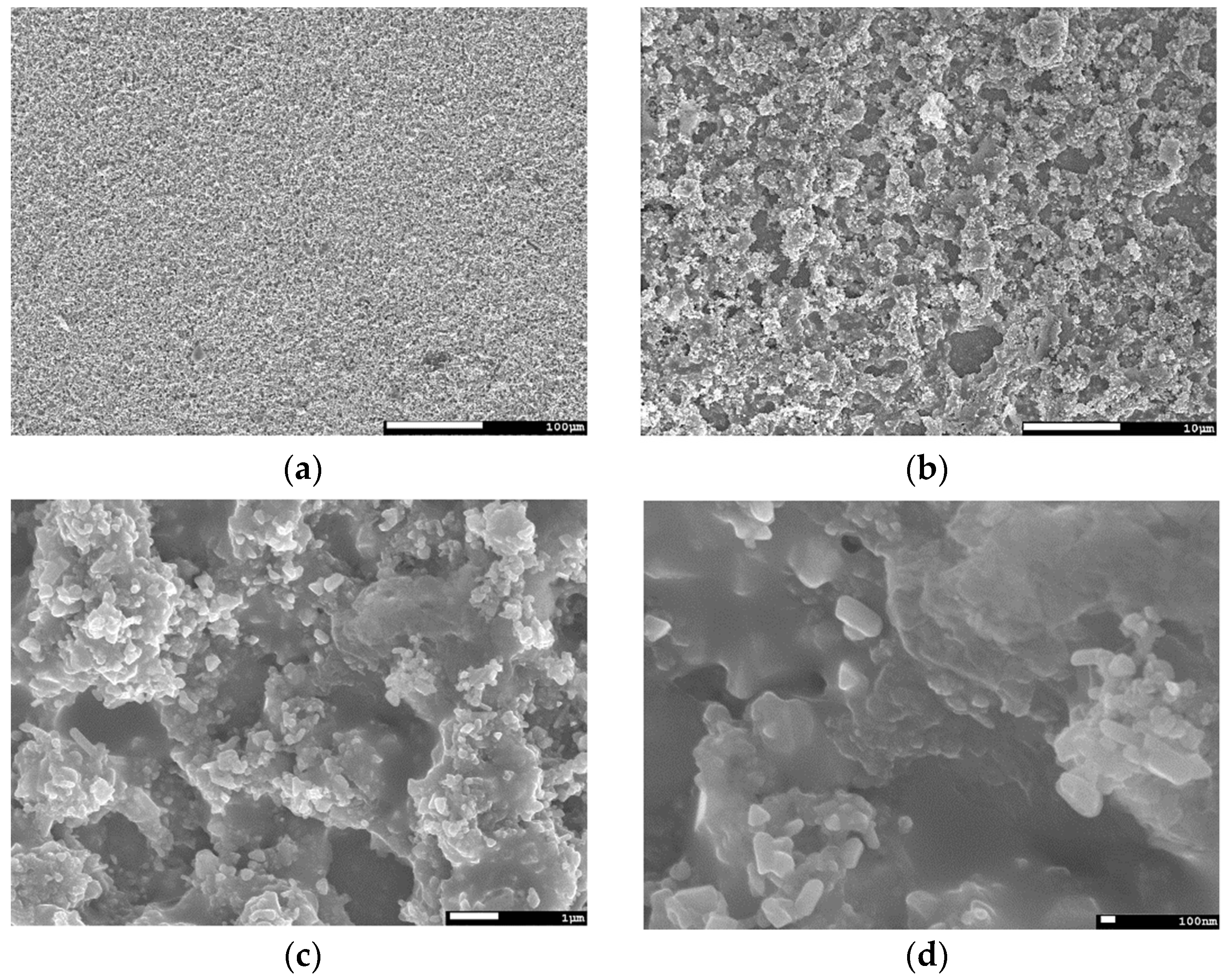
The surface morphology as seen in Figure 3a is a mostly closed layer with little surface roughness, and no damage from the face-to-face glass is visible. However, there is also a pin-hole that reaches down to the back contact. In higher magnifications of Figure 3b, the CISe looks smooth and very well sintered together, while only very few 100 nm grains remain that are connected to the µm-sized grains. A more detailed image-series of this sample is shown in Figure A1. In the pin-hole, MoSe2 can be identified with EDX (Mo: 27.0 at %; Se: 51.3 at %; O: 12.5 at %; Cu: 5.5 at %; In: 3.7 at %), thus confirming that the hole reaches the back-contact and most likely a shunt will be formed when the buffer-layer and front electrode are fabricated.
The cross-section morphology as shown in Figure 3c features a ca. 3 µm thick (as measured from the SEM image) and dense CISe layer. On the right, one of the pin-holes can also be seen, which reaches the back-contact.
In Figure A2 (see Appendix), the Tauc plot derived from UV/vis reflectivity measurements shows a band gap energy of 0.93 eV that fits to copper-poor CISe. EDX analysis shows a Cu/In ratio of 0.93: Cu: 10.3 at %; In: 11.1 at %; Se: 72.1 at %, confirming the copper-poor composition and showing the Se excess that was even visible in XRD.
In the second part of route I, the sputter-deposited Cu-In seeding layer was included in the process to study the effect of a seeding layer and an additional liquid In phase on the film formation. The thickness of 45 nm Cu and 190 nm In was chosen to result in a 200 nm CISe layer during selenization and the excess indium was equalized by coating Cu2−xSe nanoparticles before more Cu-In and Se-NPs were deposited as further precursor material.
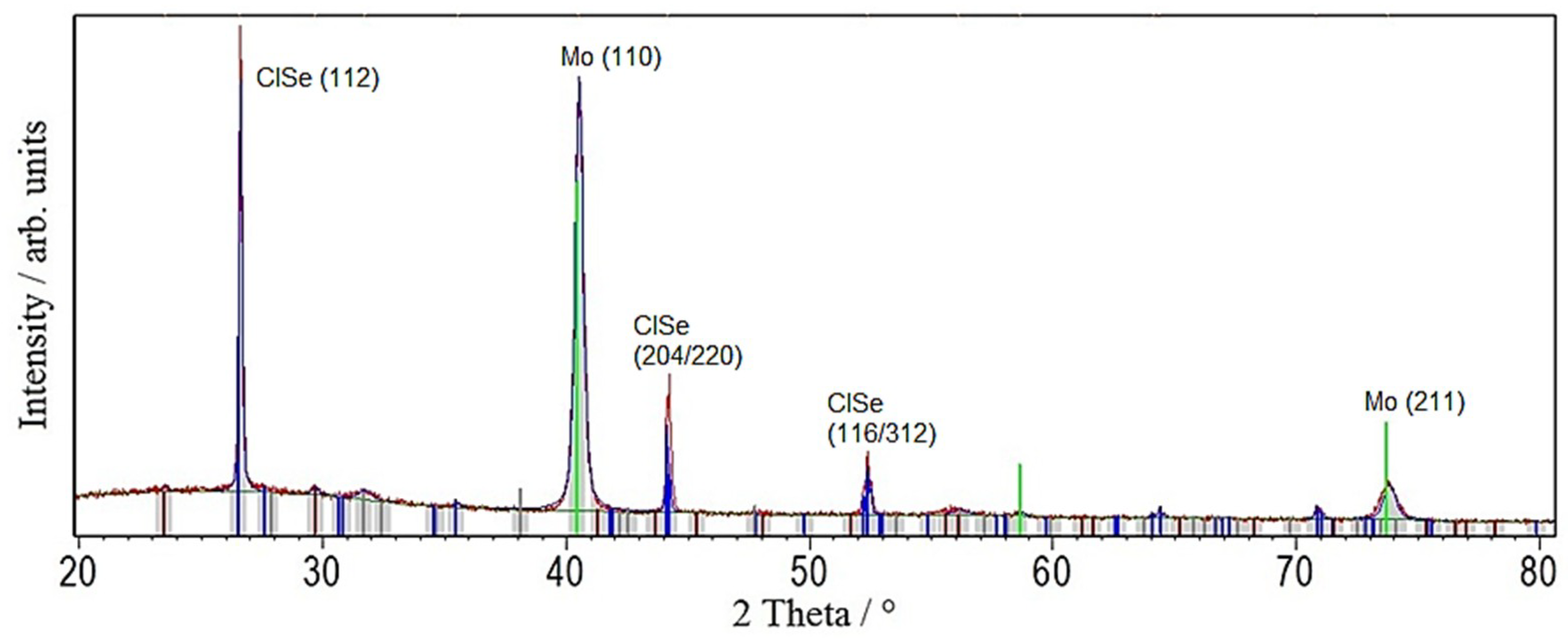
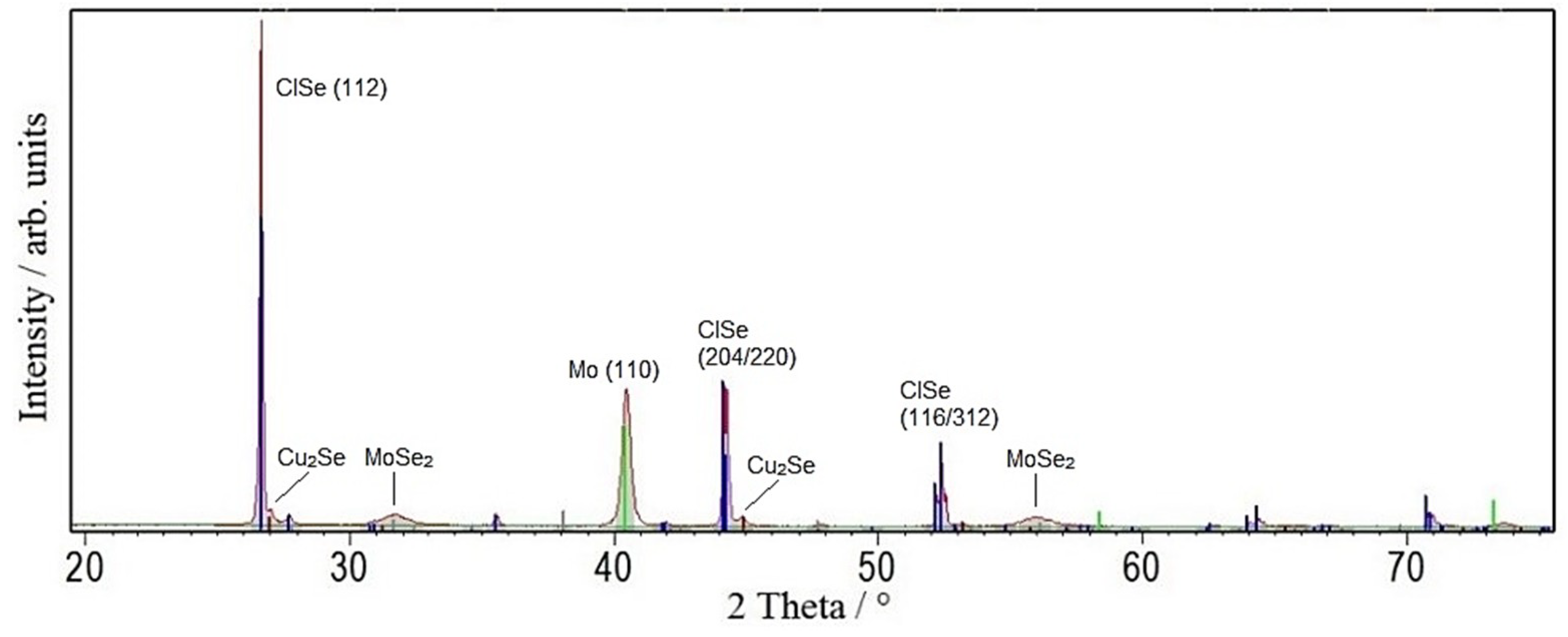
Figure 4 shows the XRD spectrum of the CISe layer from this hybrid precursor after face-to-face annealing. The CISe reflections are sharp with an FWHM of 0.13° and really strong when compared with the Mo signal, the MoSe2-phase is formed as well, and there are no indications for oxides or indium selenides. However, a small amount of copper selenide can be identified, most likely owing to a slight excess when balancing the In amount.
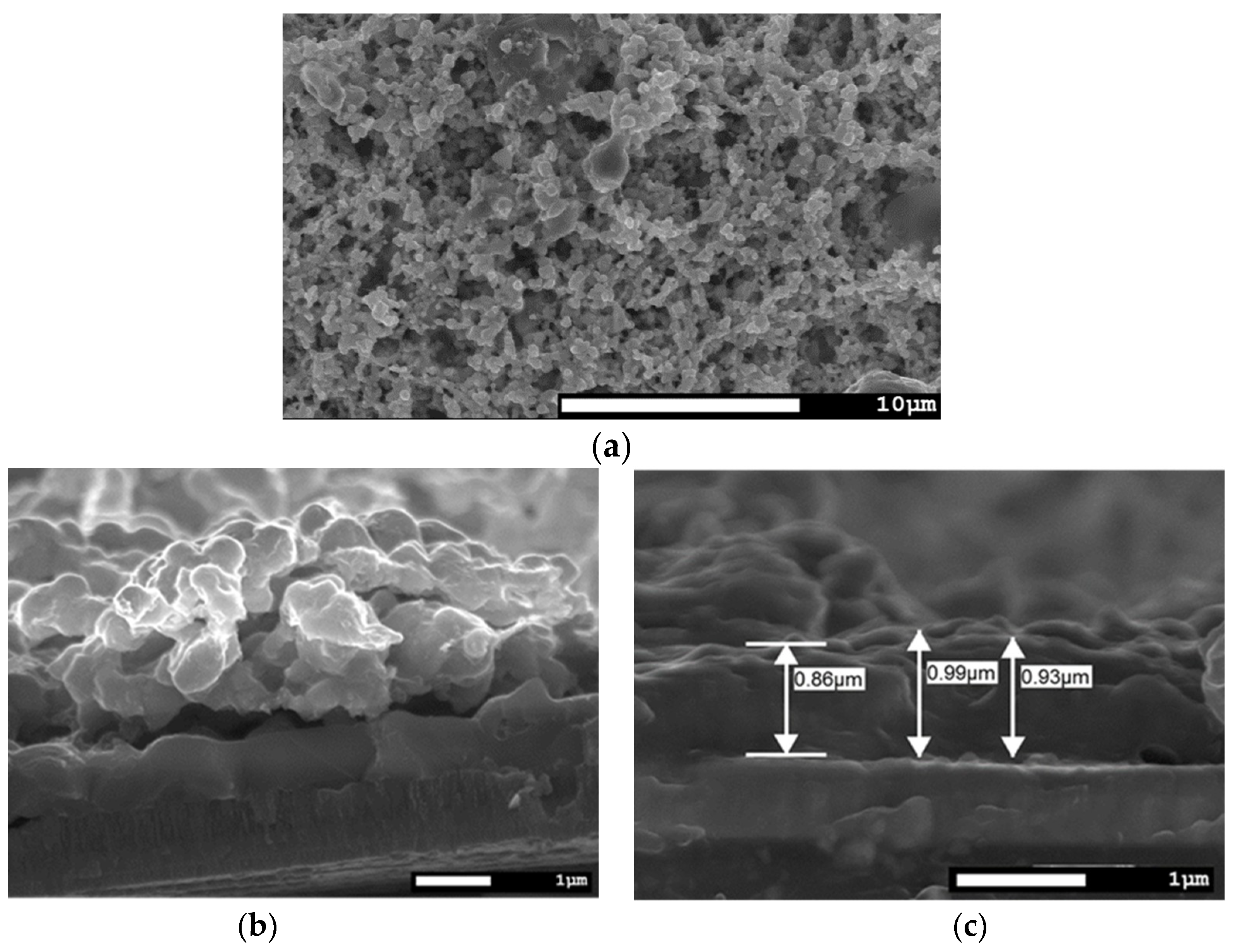
The surface morphology, as seen in Figure 5a, is comparable to the films without seeding layers, but the cross-section morphology (Figure 5b) changes a lot. In this case, on top of the back contact, a ca. 1 µm completely dense CISe film is formed from the sputtered seeding layer, which far exceeds the calculated thickness of 200 nm. Then, the morphology changes to a 2.5 µm coarse grained film. It is also to be noted that the 1 µm dense layer is found all along the cross section and no pin-holes to the back contact are present.
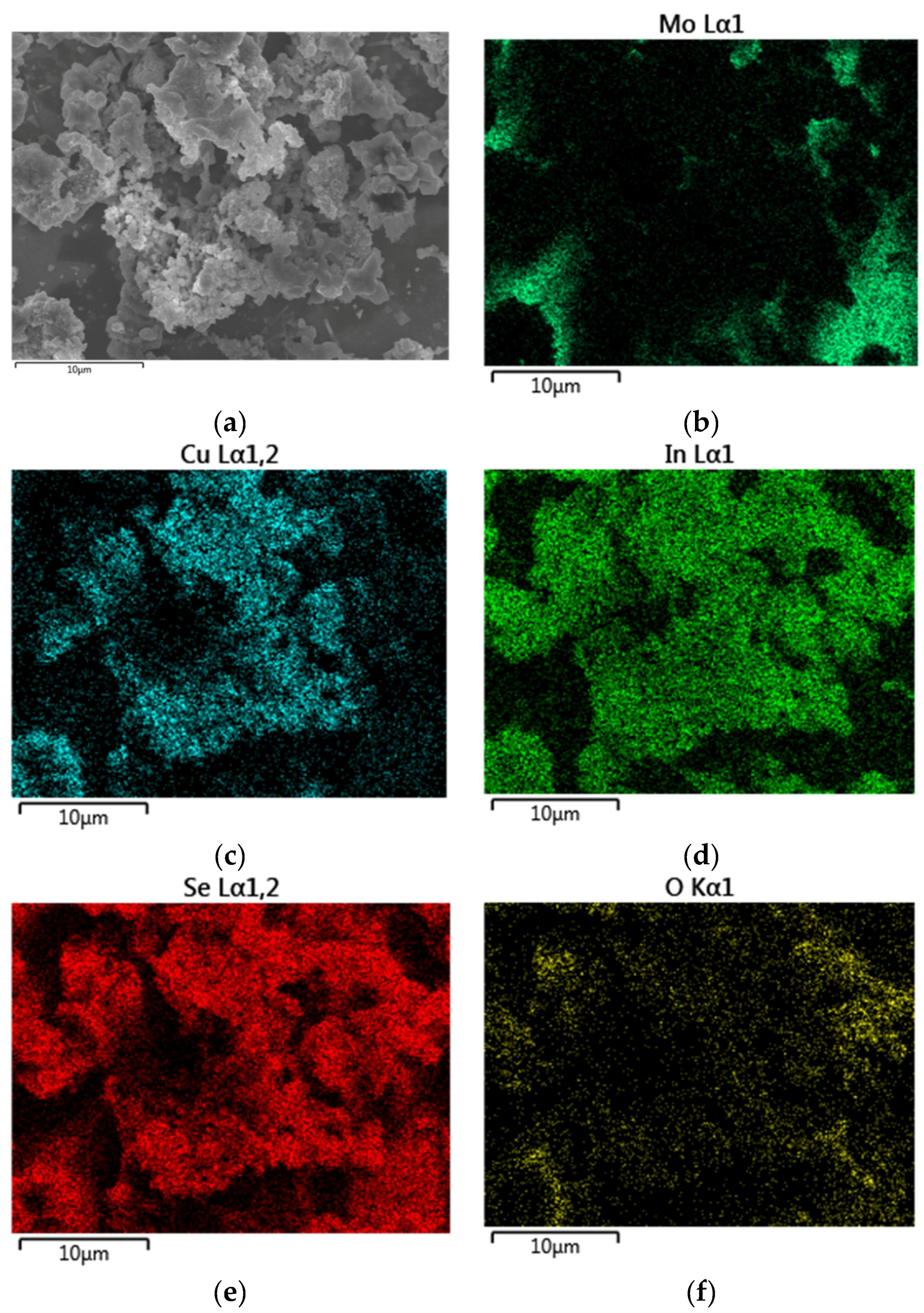
Figure A2 (Appendix) shows the Tauc plot to determine the band gap of 0.97 eV of this CISe layer, again being in the low-band-gap region, but with a Cu/In ratio closer to 1. EDX shows a copper rich (Cu/In > 1) elemental composition of Cu: 24.7 at %; In: 22.8 at %; Se: 46.7 at %; O: 3.9 at %, but as already seen in XRD, the copper excess can be explained by the Cu2Se remaining in the film. An EDX-mapping of this sample is shown in Appendix Figure A3. It can be seen that the Cu and Se distribution resemble the surface morphology, whereas In is evenly distributed over the examined area. Another EDX result from a route Ib CISe film matches the Cu/In ratio of 0.88 from the precursor: Cu: 15.1 at %; In: 17.2 at %; Se: 37.9 at %; O: 22.8 at %.

3.2. Route II

In this section, the results from the binary selenide precursors after temperature treatment are shown. The chosen selenides Cu2−xSe and In2Se3 are direct predecessors of CuInSe2 during its formation pathway and CISe formation was studied in situ [19].
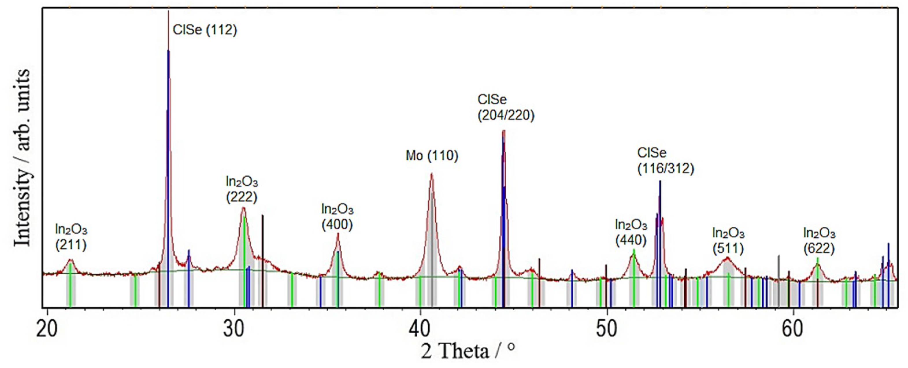
The XRD spectrum in Figure 6 shows sharp CISe reflections with an FWHM of 0.13° and the Mo back contact, but also huge amounts In2O3.
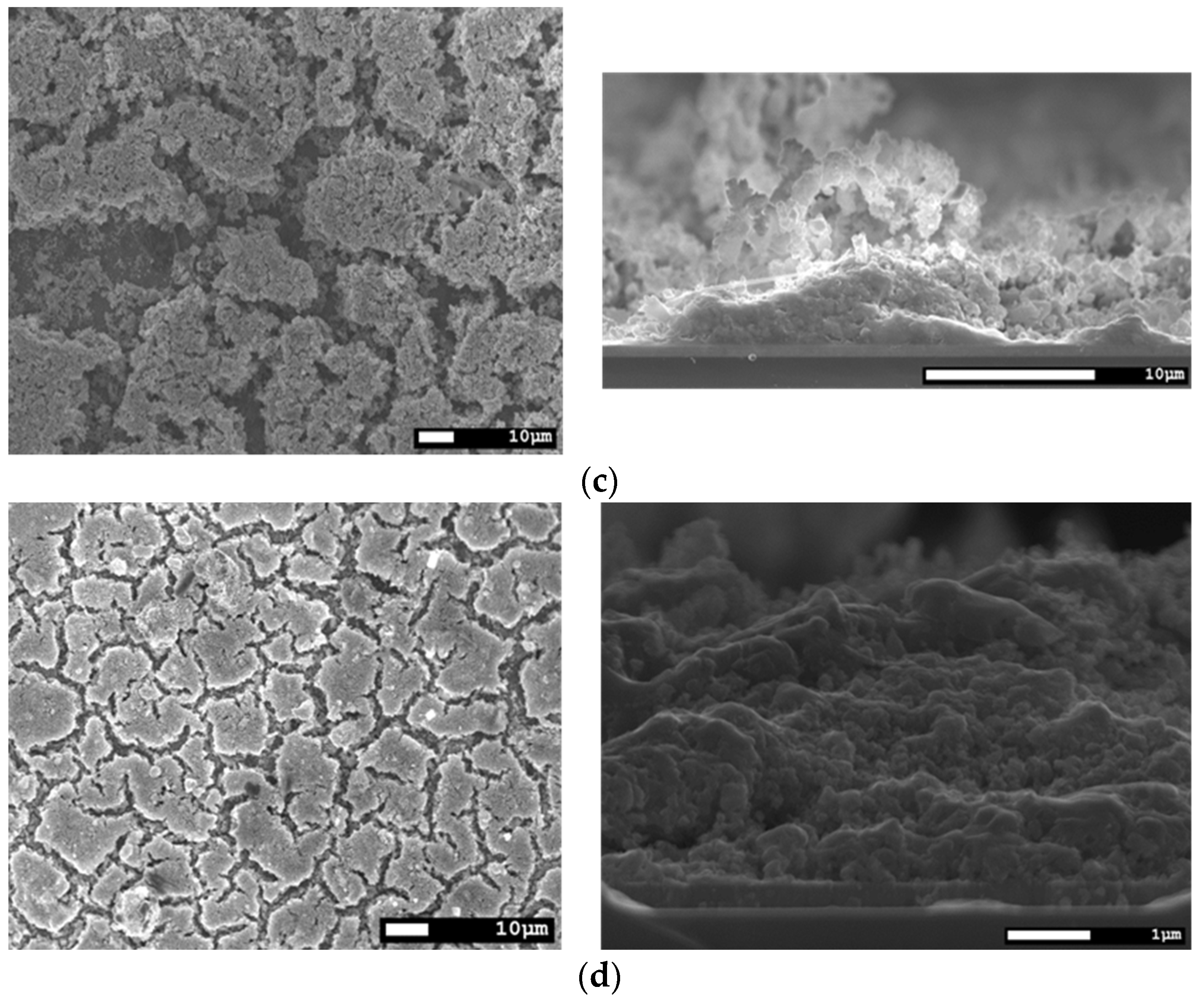
In Figure 7, the surface and cross-section morphologies of CISe films from selenide precursors after different temperature treatments are shown. As can be seen, the face-to-face annealing with application of pressure (a) does not work as well as for the route I precursors. Drying cracks are visible in all of the respective layers, but they are most prominent in the sample processed by face-to-face annealing (a). Temperature treatment without any pressure (b) did work better considering surface area coverage, but the benefit of face-to-face can still be seen in the cross-section images. In the spots where grains were formed, they are better sintered together and less porous than in the sample from the tube furnace. In both samples, the drying cracks reach the back contact and will result in shunts once the buffer- and window-layer are applied. An improvement in surface coverage and cross-section morphology was achieved by repeating the coating and face-to-face annealing process two times (c). The cracks no longer reach the back contact, but are still large and inconsistently uncovered areas. Another possibility for improvement was the use of an ethanol based nano-ink instead of isopropanol. This makes use of the better wetting, coating and drying properties of ethanol owing to its significantly lower viscosity, slightly lower surface tension, and slightly lower boiling point, while having almost the same density as IPA. In this sample (d), the surface coverage is the best out of all the variants and in the cross-section, the layer looks densely sintered together even without application of pressure.
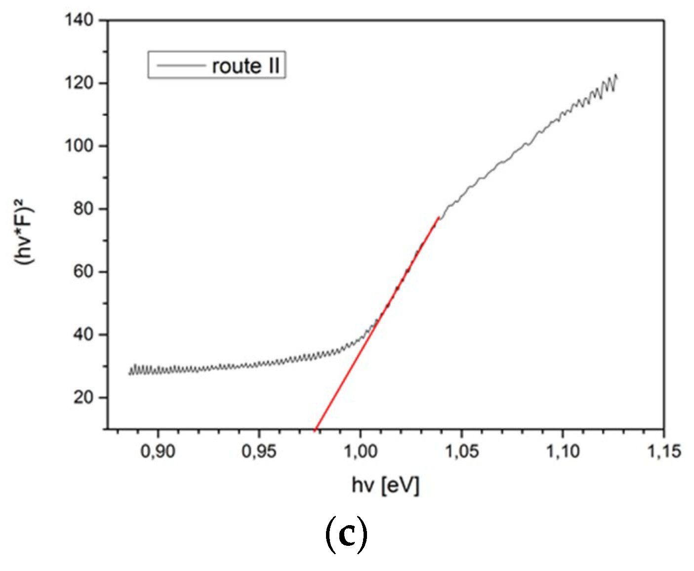
The band gap energy of a route II CISe film was found to be 0.98 eV. The corresponding Tauc plot is shown in Figure A2 (Appendix). The elemental composition measured with EDX shows a slightly copper-poor composition with a Cu/In ratio of 0.92: Cu: 18.6 at %; In: 20.3 at %; Se: 43.5 at %; O: 17.5 at %. The EDX mapping (see Appendix Figure A4) shows an evenly distributed elemental composition and a smooth surface of the CISe film.
An EDX mapping of another sample from the same series, but with a Cu/In ratio of 0.88, is shown in Figure A5 (Appendix): Cu: 15.5 at %; In: 17.6 at %; Se: 32.1 at %; O: 7.7 at %. The molybdenum is clearly seen, where no CISe film covers the back electrode. Cu and Se again resemble the surface morphology and In is evenly distributed in the CISe film.

4. Discussion

In route Ia, by annealing the nanoparticle precursors in the N2-atmosphere, and thus excluding oxygen from air, nanoparticle oxidation can be prevented as verified by XRD. In a regular atmosphere, oxidation happens easily at elevated temperatures, especially for indium. Oxide layers surrounding the nanoparticles would hinder the reactions and diffusion processes and promote a more porous morphology with more nano-sized grains and remaining selenides. Additionally, the applied pressure helps to condense the precursor film, even more so once the Se melts. Capillary forces rearrange the nanoparticles, and thus the CISe film quality is enhanced by liquid phase and pressure sintering. Complete transformation of the nanoparticle precursor into a dense CISe layer in 5 min, as well as an absence of oxides and selenides, shows the potential of the face-to-face annealing with external pressure for solar cell manufacturing, especially if the formation of pin-holes can be prevented and the surface smoothness can be enhanced. Also, there is no need for external Se atmosphere or H2Se gas, as all the Se is directly in the precursor and does not evaporate and leave the face-to-face sandwich. Should an excess of Se or copper selenides be present in the film, it can easily be removed by KCN or even better by ammonium sulfide (NH4)2S treatment [22]. Absorbers with band gap energies below 1 eV like this have been used in tandem solar cells [11], once the surface morphology is better optimized in terms of smoothness and porosity.
When using the sputter-deposited seeding layer in route Ib, it can be concluded that during the face-to-face annealing with applied pressure, two liquid phases of In and Se exist one after the other in the temperature region of their respective melting points, and the rearrangement of nanoparticles can occur twice. Aided by pressure sintering, the Cu-In and Se precursor continues to grow in the dense morphology provided by the sputtered seeding layer, as long as both liquid phases and the Cu2−xSe phase are present. Here, the 200 nm dense CISe calculated from the sputtered Cu grows to almost five times the thickness. In the top region of the precursor, only Se can contribute to the liquid phase sintering and there is no Cu2−xSe present at the start of the annealing process, so the resulting morphology resembles the commonly known coarse grained CISe. To achieve a completely vacuum-free route Ib CISe layer, elemental Cu and In NPs could be used as well as very indium rich, bimetallic Cu-In NPs to form the seeding layer and provide the liquid indium. The below 1 eV band gap energies of these samples again allow for application in tandem solar cells [11], once the morphology is optimized.
Route II showed several hindering mechanisms when compared with route I. The remaining In2O3 most likely stems from the partly oxidation of the indium selenide nanoparticles before the coating process, which was observed as a change in dispersion-color and with EDX measurements in SEM. Therefore, diffusion processes and chemical reactions are hindered and a complete transformation of the precursor was prevented. This could be overcome by an excess of Se NP, as In2O3 has been transformed back to selenide in earlier work [23,24], which can continue the reaction to CISe and consume the possibly left-over Cu2−xSe. The morphology of the final film needs even more optimization compared with route I in terms of surface coverage and porosity. This is mostly because of the lack of a liquid phase during the reaction. There is no beneficial particle rearranging by capillary forces to densify the film. Even though, with application of external pressure, a densification of certain areas was observed, the porosity accumulates at the drying cracks and thus widens them. Improvement was achieved by repeating the coating and annealing processes. In this way, the nanoparticles from the second coating filled up the drying cracks left in the layer after the first annealing, and the film quality in terms of surface coverage was enhanced. The best quality, however, was found in a sample derived from ethanol-based nano-inks, which used the better wetting behavior of ethanol compared with isopropanol owing to its significantly lower viscosity, slightly lower surface tension, and slightly lower boiling point. The dispersion stability of the nanoparticles between IPA and ethanol did not vary significantly. In this sample, the surface coverage is the best out of all the variants and, in the cross section, the layer looks densely sintered together even without application of pressure or the presence of a liquid phase, suggesting that the packing of precursor nanoparticles is much better compared with the IPA-ink. Route II, however, needs more improvement before the CISe-layers reach absorber quality, although the band gap energy of the slightly copper-poor film is 0.98 eV and again shows potential for low-band-gap applications.

5. Conclusions

In this work, two different routes were examined to manufacture dense and homogenous low-band-gap CISe thin-films using nanoparticle based precursors. In route I, the face-to-face-method with application of external pressure was used at a temperature of 550 °C to form 3 µm homogenous and dense CISe-layers from bimetallic Cu-In and elemental Se nanoparticles. A 200 nm dense CISe film was prepared from a sputtered Cu and In seeding layer that continued to grow from addition of nano-ink up to 1 µm completely dense and closed before transitioning into a coarse grained morphology. A vacuum-free seeding layer can be achieved with elemental Cu and In NP or indium rich Cu-In bimetallic NP. Both CISe-layers from route I show low-band-gap energies of 0.93–0.97 eV and might be used as a solar cell absorber if the film quality in terms of porosity and smoothness is enhanced. This shows the prospect of a simple continuous coating process on infinite substrates and roll-to-roll machines for the temperature treatment with application of pressure.
Route II, which uses binary Cu2−xSe and In2Se3 nanoparticles, results in partly closed layers with drying cracks and large amounts of remaining In2O3. Using ethanol instead of isopropanol for nano-ink formulation or repeating the coating and annealing process improves the layer quality in terms of both surface and cross-section morphology. Nevertheless, for route II, more optimization is necessary, before any use as solar cell absorber is feasible.

Author Contributions

Conceptualization of experiments, M.S.; Performing experiments and acquiring results, M.S., D.S., T.O., and V.B.; Writing—original draft preparation and editing, M.S.; Writing—review, P.J.W.; Project administration, P.J.W.

Funding

This research was funded by the German Federal Ministry for Economic Affairs and Energy (Bundesministerium für Wirtschaft und Energie) for financial support under the contract MYCIGS.

Conflicts of Interest

The authors declare no conflict of interest.

Appendix A

Figure A1. Scanning electron microscopy (SEM) top view image series of a CuInSe2 (CISe)-film from Cu-In + Se precursor after face-to-face annealing at 550 °C for 5 min with 46.1 kN/m2 at different magnifications, (a) 200×; (b) 2,000×; (c) 10,000×; (d) 30,000×.
Coatings 09 00484 g0a1
Figure A2. Tauc plots of different CISe-film samples derived form reflectivity measurements. (a) From Cu-In + Se precursor after face-to-face annealing at 550 °C for 5 min with 46.1 kN/m2 pressure. (b) From Cu-In + Se precursor with seeding layer after face-to-face annealing at 550 °C for 5 min with 46.1 kN/m2 pressure. (c) From Cu2−xSe + In2Se3 precursor after face-to-face annealing at 550 °C for 5 min with 46.1 kN/m2 pressure.
Coatings 09 00484 g0a2aCoatings 09 00484 g0a2b
Figure A3. Energy dispersive X-ray spectroscopy (EDX) mapping (a) of route Ib CISe film with an elemental composition of Cu: 24.7 at % (b); In: 22.8 at % (c); Se: 46.7 at % (d); O: 3.9 at % (e).
Coatings 09 00484 g0a3
Figure A4. EDX mapping (a) of ethanol based route II CISe film shows an evenly distributed elemental composition of Cu: 18.6 at % (b); In: 20.3 at % (c); Se: 43.5 at % (d); O: 17.5 at % (e).
Coatings 09 00484 g0a4
Figure A5. EDX mapping (a) of IPA based route II CISe film with an elemental composition of Cu: 15.5 at % (c); In: 17.6 at % (d); Se: 32.1 at % (e); O: 7.7 at % (f). Mo of back contact (b) is visible where the CISe film does not cover the back electrode.
Coatings 09 00484 g0a5

References

  1. Green, M.A.; Hishikawa, Y.; Dunlop, E.D.; Levi, D.H.; Green, M.A.; Hohl-Ebinger, J.; Yoshita, M.; Ho-Baillieet, A.W.Y. Solar cell efficiency tables (Version 53). Prog. Photovolt Res. Appl. 2019, 27, 3–12. [Google Scholar] [CrossRef]
  2. Singh, M.; Prasher, P.; Suganuma, K. Fabrication of dense CIGS film by mixing two types of nanoparticles for solar cell application. Nano-Struct. Nano-Objects 2017, 11, 129–134. [Google Scholar] [CrossRef]
  3. Yu, H.; Hsing, L. Dense CIGS films obtained by blending submicron-sized particles with nanoparticle suspensions using a non-vacuum process. Int. J. Appl. Ceram. Technol. 2019, 16, 974–980. [Google Scholar] [CrossRef]
  4. Arnou, A.P.; Bowers, J.W.; Walls, J.M.; Whitelegg, S.; Kirkham, P.; Allen, C.; Stubbs, S.; Liu, Z.; Masala, O.; Newman, C.; et al. High-efficiency nanoparticle solution-processed Cu(In,Ga)(S,Se)2 solar cells. IEEE J. Photovolt. 2018, 8, 288–292. [Google Scholar] [CrossRef]
  5. McLeod, S.M.; Hages, C.J.; Carter, N.J.; Agrawal, R. Synthesis and characterization of 15% efficient CIGSSe solar cells from nanoparticle inks. Prog. Photovolt. Res. Appl. 2015, 23, 1550–1556. [Google Scholar] [CrossRef]
  6. Park, G.S.; Chu, V.B.; Kim, B.W.; Kim, D.; Oh, H.-S.; Hwang, Y.J.; Hwang, Y.J.; Min, B.K. Achieving 14.4% alcohol-based solution-processed Cu(In,Ga)(S,Se)2 thin film solar cell through interface engineering. ACS Appl. Mater. Interfaces 2018, 10, 9894–9899. [Google Scholar] [CrossRef]
  7. Barbé, J.; Eid, J.; Ahlswede, E.; Spiering, S.; Powalla, M.; Agrawal, R.; Gobbo, S.D. Inkjet printed Cu(In,Ga)S2 nanoparticles for low-cost solar cells. J. Nanoparticle Res. 2016, 18, 379. [Google Scholar] [CrossRef]
  8. Tiwari, D.; Koehler, T.; Lin, X.; Sarua, A.; Harniman, R.; Wang, L.; Klenk, R.; Fermin, D.J. Single molecular precursor solution for CuIn(S,Se)2 thin films photovoltaic cells: Structure and device characteristics. ACS Appl. Mater. Interfaces 2017, 9, 2301–2308. [Google Scholar] [CrossRef]
  9. Lin, X.; Klenk, R.; Wang, L.; Köhler, T.; Albert, J.; Fiechter, S.; Ennaoui, A.; Lux-Steiner, M.C. 11.3% efficiency Cu(In,Ga)(S,Se)2 thin film solar cells: Via drop-on-demand inkjet printing. Energy Environ. Sci. 2016, 9, 2037–2043. [Google Scholar] [CrossRef]
  10. Romanyuk, Y.E.; Hagendorfer, H.; Stücheli, P.; Fuchs, P.; Uhl, A.R.; Sutter-Fella, C.M.; Werner, M.; Haass, S.; Stückelberger, J.; Broussillou, C.; et al. All solution—Processed chalcogenide solar cells—From single functional layers towards a 13.8% efficient CIGS device. Adv. Funct. Mater. 2015, 25, 12–27. [Google Scholar] [CrossRef]
  11. Elanzeery, H.; Babbe, F.; Melchiorre, M.; Werner, F.; Siebentritt, S. High-performance low bandgap thin film solar cells for tandem applications. Prog. Photovolt. Res. Appl. 2018, 26, 437–442. [Google Scholar] [CrossRef] [Green Version]
  12. Chen, G.; Wang, L.; Sheng, X.; Liu, H.; Pi, X.; Yang, D. Chemical synthesis of Cu(In) metal inks to prepare CuInS2 thin films and solar cells. J. Alloys Compd. 2010, 507, 317–321. [Google Scholar] [CrossRef]
  13. Chang, J.; Lee, J.H.; Cha, J.H.; Jung, D.Y.; Choi, G.; Kim, G. Bimetallic nanoparticles of copper and indium by borohydride reduction. Thin Solid Films 2011, 519, 2176–2180. [Google Scholar] [CrossRef]
  14. Schuster, M.; Möckel, S.A.; Wibowo, R.A.; Hock, R.; Wellmann, P.J. Optimising the parameters for the synthesis of CuIn-nanoparticles by chemical reduction method for chalcopyrite thin film precursors. MRS 2013, 1538, 203–208. [Google Scholar] [CrossRef]
  15. Stroyuk, A.L.; Raevskaya, A.E.; Kuchmiy, S.Y.; Dzhagan, V.M.; Zahn, D.R.T.; Schulze, S. Structural and optical characterization of colloidal Se nanoparticles prepared via the acidic decomposition of sodium selenosulfate. Colloids Surf. A Physicochem. Eng. Asp. 2008, 320, 169–174. [Google Scholar] [CrossRef]
  16. Ingole, A.R.; Thakare, S.R.; Khati, N.T.; Wankhade, A.V.; Burghate, D.K. Green synthesis of selenium nanoparticles under ambient condition. Chalcogenide Lett. 2010, 7, 485–489. [Google Scholar]
  17. Schuster, M.; Wernicke, T.; Möckel, S.A.; Wellmann, P.J. Determination of the molar extinction coefficient of colloidal Selenium for optical characterization of stabilized nanoparticulate dispersions. Int. J. Nanoparticles Nanotechnol. 2016, 2, 1–8. [Google Scholar] [CrossRef]
  18. Zhang, W.; Zhang, X.; Zhang, L.; Wu, J.; Hui, Z.; Cheng, Y.; Liu, J.; Xie, Y.; Qian, Y. A redox reaction to synthesize nanocrystalline Cu2−xSe in aqueous solution. Inorg. Chem. 2000, 39, 1838–1839. [Google Scholar] [CrossRef]
  19. Schuster, M.; Distaso, M.; Möckel, S.A.; Künecke, U.; Peukert, W.; Wellmann, P.J. Synthesis of In2Se3 and Cu2−xSe micro- and nanoparticles with microwave—Assisted solvothermal and aqueous redox reactions for the preparation and stabilization of printable precursors for a CuInSe2 solar cell absorber layer. Energy Proced. 2015, 84, 62–70. [Google Scholar] [CrossRef]
  20. Min, Y.; Moon, G.D.; Park, J.; Park, M.; Jeong, U. Surfactant-free CuInSe2 nanocrystals transformed from In2Se3 nanoparticles and their application for a flexible UV photodetector. Nanotechnology 2011, 22, 46560. [Google Scholar] [CrossRef]
  21. Schuster, M.; Sisterhenn, P.; Graf, L.; Wellmann, P.J. Processing and characterization of vacuum-free CuInSe2 thin films from nanoparticle—Precursors using novel temperature treatment techniques. Int. J. Nanopart. Res. 2018, 2, 1–10. [Google Scholar]
  22. Buffière, M.; Mel, A.A.E.; Lenaers, N.; Brammertz, G.; Zaghi, A.E.; Meuris, M.; Poortmans, J. Surface cleaning and passivation using (NH4)2S treatment for Cu(In,Ga)Se2 solar cells: A safe alternative to KCN. Adv. Energy Mater. 2015, 5, 1401689. [Google Scholar] [CrossRef]
  23. Möckel, S.A.; Hölzing, A.; Hock, R.; Wellmann, P.J. In-situ phase formation study of copper indium diselenide absorber layers from CuIn nanoparticles and evaporated selenium. Thin Solid Films 2013, 353, 133–137. [Google Scholar] [CrossRef]
  24. Pulgarín-Agudelo, F.; López-Marino, S.; Fairbrother, A.; Placidi, M.; Pina, B.; Saucedo, E. A thermal route to synthesize photovoltaic grade CuInSe2 films from printed CuO/In2O3 nanoparticle-based inks under Se atmosphere. J. Renew. Sustain. Energy 2013, 5, 053140. [Google Scholar] [CrossRef]
Figure 1. Schematic overview on the experimental processes, showing details of nanoparticle synthesis, nano-inks for process routes I and II, as well as a schematic of the face-to-face process. Route Ia uses only ink I from Cu-In and Se NP, route Ib uses an additional sputtered Cu-In seeding layer, route II uses ink II from In2Se3 and Cu2-xSe NP and additional Se NP. SEM, scanning electron microscopy; EDX, energy dispersive X-ray spectroscopy; XRD, X-ray diffraction; EDTA, ethylenediaminetetraacetic acid; TEG, tetra ethylene glycol; PVP, polyvinylpyrrolidone.
Coatings 09 00484 g001
Figure 2. XRD pattern of a CuInSe2 (CISe)-film from Cu-In + Se nanoparticle precursor after face-to-face annealing at 550 °C for 5 min with 46.1 kN/m2 pressure.
Coatings 09 00484 g002
Figure 3. (a) SEM top view of a CISe-film from Cu-In + Se nanoparticle precursor after face-to-face annealing at 550 °C for 5 min with 46.1 kN/m2 pressure shows a homogenous, but rough surface with a hole. (b) Higher magnification image of the same sample shows well sintered grains. (c) Cross-section image of the same sample shows a 3 µm dense layer with a hole to the back-contact.
Coatings 09 00484 g003aCoatings 09 00484 g003b
Figure 4. XRD pattern of a CISe-film from Cu-In + Se nanoparticle precursor with a sputter-deposited seeding layer after face-to-face annealing at 550 °C for 5 min with 46.1 kN/m2 pressure.
Coatings 09 00484 g004
Figure 5. SEM images of a CISe-film from Cu-In + Se nanoparticle precursor with a sputter-deposited seeding layer after face-to-face annealing at 550 °C for 5 min with 46.1 kN/m2 pressure. (a) Top view image comparable to route Ia. (b) Cross-section image shows a dense CISe film from the seeding layer and on top a ca. 2.5 µm thick coarse grained CISe film. (c) Cross-section close up of dense CISe film from the sputtered seeding layer with ca. 1 µm thickness.
Coatings 09 00484 g005
Figure 6. XRD pattern of a CISe-film from Cu2−xSe + In2Se3 nanoparticle precursor after the repetition of coating and annealing at 550 °C for 5 min shows huge amounts of In2O3 in the film.
Coatings 09 00484 g006
Figure 7. SEM top view and cross-section of a CISe-film from Cu2−xSe + In2Se3 nanoparticle precursor after different temperature treatments. (a) Face-to-face annealing at 550 °C for 5 min with 46.1 kN/m2 pressure. (b) Annealing in the tube furnace at 550 °C for 5 min without application of pressure. (c) Two times repetition of ink-coating and face-to-face annealing at 550 °C for 5 min with 46.1 kN/m2 pressure. (d) Using an ethanol based nano-ink and annealing in the tube furnace at 550 °C for 5 min without application of pressure.
Coatings 09 00484 g007aCoatings 09 00484 g007b