1. Introduction
Steadily raising power in laser material processing, finer and finer structures in semiconductor lithography and state-of-the-art optical components are faced with increasing demands and requirements. Absorption, being one of the key parameters in high-end laser applications, is gaining more and more attention due to the undesired effects resulting from thermal lensing like focus shifting, wave front deformation and depolarization. In order to take these critical issues into account in modern optic design, highly sensitive absorption measurement techniques in combination with reliable absolute calibration are required.
Commonly, measuring spectral reflectance and transmittances is the method of choice to investigate optical losses of thin films, followed by a calculation of the optical constants e.g., the refractive index
n and extinction coefficient
k. However, extinction coefficients obtained by that procedure contain both scatter and absorption contributions because it is not feasible to separate these parts by simply measuring transmission and reflection spectra. For particular applications, however, individual absorption and scattering data are strongly required due to their different potential interferences on the optical system performance. Further, bulk and coating/surface effects need to be separated to discriminate between different origins of absorption and scattering, respectively. Consequently, direct absorption measuring in optical thin films and bulk materials have gained more and more attention in optics qualification to ensure or improve stabile production processes, to prepare particular optical functionalities and to identify potential show stoppers upon use in high-end laser applications. Following this increasing demand, a variety of direct absorption measurement techniques have been developed recently featuring—despite particular pros and cons—a high sensitivity [
1,
2,
3,
4,
5]. Providing not only relative but absolute absorption data has recently become more and more important e.g., in order to quantitatively simulate complex optical systems. However, with respect to an absolute calibration, the various direct absorption measurement techniques show remarkable differences when it comes to a universal and efficient procedure.
This paper will give an introduction of the laser induced deflection (LID) technique and its independent absolute calibration for the characterization of optical thin films. Further, particular LID measurement concepts are presented together with experimental results.
2. Materials and Methods
2.1. Laser Induced Deflection (LID) Technique
The laser induced deflection (LID) technique belongs to an ensemble of photo-thermal techniques with a pump-probe-configuration [
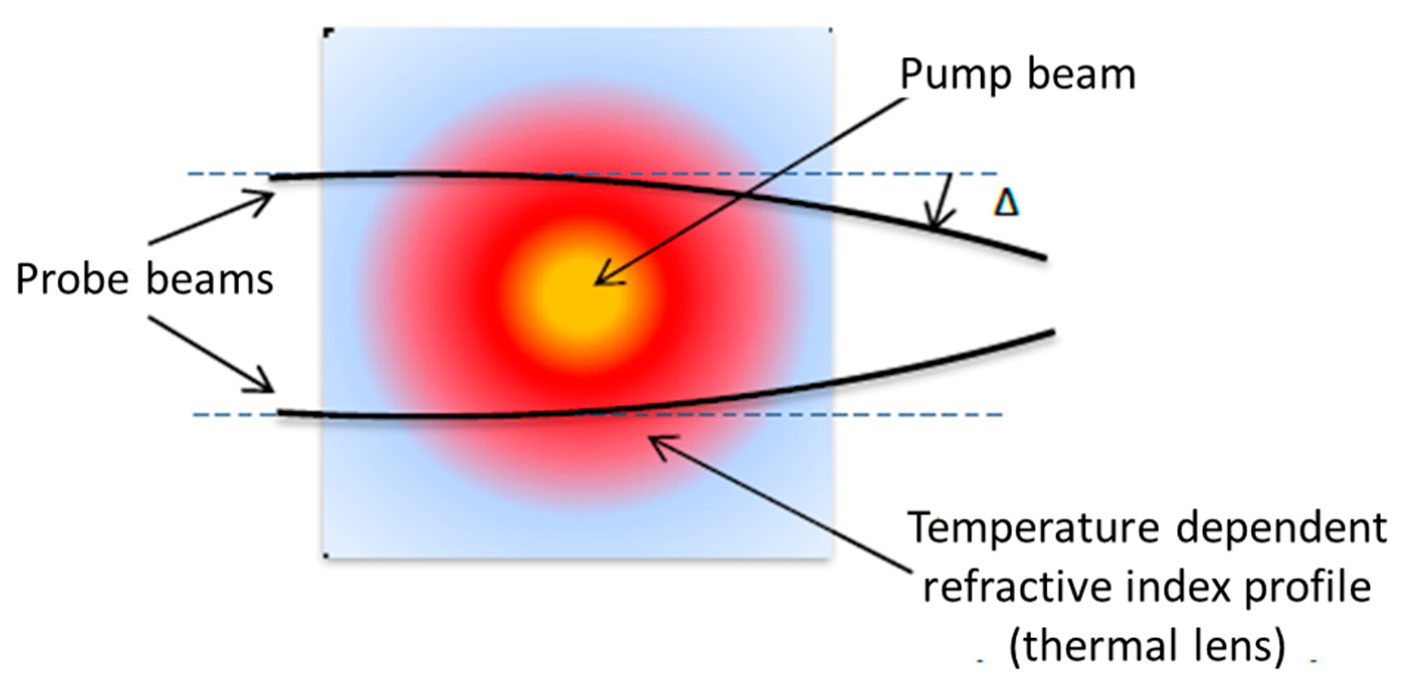
6]. When the pump laser hits the sample under investigation, the absorbed pump laser power forms a temperature profile (
Figure 1). The latter is turned into a refractive index profile (= thermal lens) by both the thermal expansion and the temperature dependent refractive index, respectively. The refractive index gradient accounts for a deflection of the probe beams (from the same laser source), that is proportional to the absorbed pump laser power.
In the case of the LID technique, the deflection for each probe beam is detected separately by two-dimensional position sensitive detectors (PSD). The total measuring signal comprises of the sum of both PSD signals. Since the deflection directions on the PSDs have opposite signs for the two probe beams (
Figure 1), the two signals are mathematically subtracted from each other. As a result, any measurement perturbations resulting from the probe laser source are strongly reduced for signal-to-noise enhancement. In combination with high averaging and the subsequent electronics, probe beam deflections in the range of some tens of Nanometers are detectable. Contrary to the majority of applied photo-thermal techniques, the LID technique uses a transversal configuration between pump and probe beam, i.e., the probe beam passes the sample under 90° to the pump beam. Thereby, in most cases crossing pump and probe beams is avoided. Instead the probe beam passes the sample outside the pump beam area. Since the refractive index profile outside the pump beam area is a function of the absorbed pump laser power only, the LID measuring signal is independent on the geometry of the pump laser beam. As another different feature compared to other photo-thermal techniques, the pump beam is not focused into the sample and typically has a larger beam size than the probe beam.
The LID measurement data is not obtained on a laser pulse-by-pulse basis. Instead, the probe beam position change with irradiation time is steadily registered with high sampling rate (16 kHz range) until it reaches its steady-state, i.e., the absorption induced refractive index gradient stays constant. To obtain a high accuracy, averaging is applied resulting in one data point every half a second. Due to the rather long data acquisition (0.5 s) and total measurement time (tens to hundreds of seconds), the deflection signal is only a function of the average absorbed pump laser power. Therefore, the actual operation mode (pulsed or continuous wave) of the pump laser does not affect the outcome of the measurement as long as the sample absorption and mean pump laser power is identical. In addition, lamps instead of laser sources can be applied as pump light source as long as the light can be shaped to an mm-size spot on the sample. Compared to alternative photo-thermal techniques, it is not required to temporally shape a pump laser operating in continuous wave mode. Furthermore, the pump laser pulse duration is not of importance for the LID measurement itself. However, the pump laser operation mode can strongly influence the sample absorption e.g., due to nonlinear absorption. This of course needs to be taken into account when choosing the pump laser source.
The LID technique itself is not limited by the pump laser wavelength as long as the average power of the pumping light is sufficient to detect the sample’s absorption. A limiting factor is the wavelength of the probe laser if the investigated sample/substrate is not transparent. Here, a change of the probe beam wavelength or the use of a particular LID measuring concept (see
Section 2.3.3) is required.
2.2. Absolute Calibration
Absolute calibration is a key figure of merit in photo-thermal absorption measurement techniques. For the LID technique, the approach of the calorimetry—electrical calibration—has been transferred for the first time to photo-thermal techniques. To obtain the absolute absorption value out of the LID measurement data, the thermal lens is generated by particular electric heaters. Since the shape of the thermal lens is different for bulk and coating (surface) absorption, both need to be calibrated separately for each combination of sample material and geometry [
7]. In case of coating/surface absorption, small surface-mount-device (SMD) elements—fixed onto a very thin copper plate (thickness ~200 µm)—are placed centrally onto the sample surface (
Figure 2). The copper plate allows for the required high thermal conduction to the sample. This calibration procedure can only be applied to transversal pump-probe configurations where the probe beam is not guided through the irradiated/heated sample part.
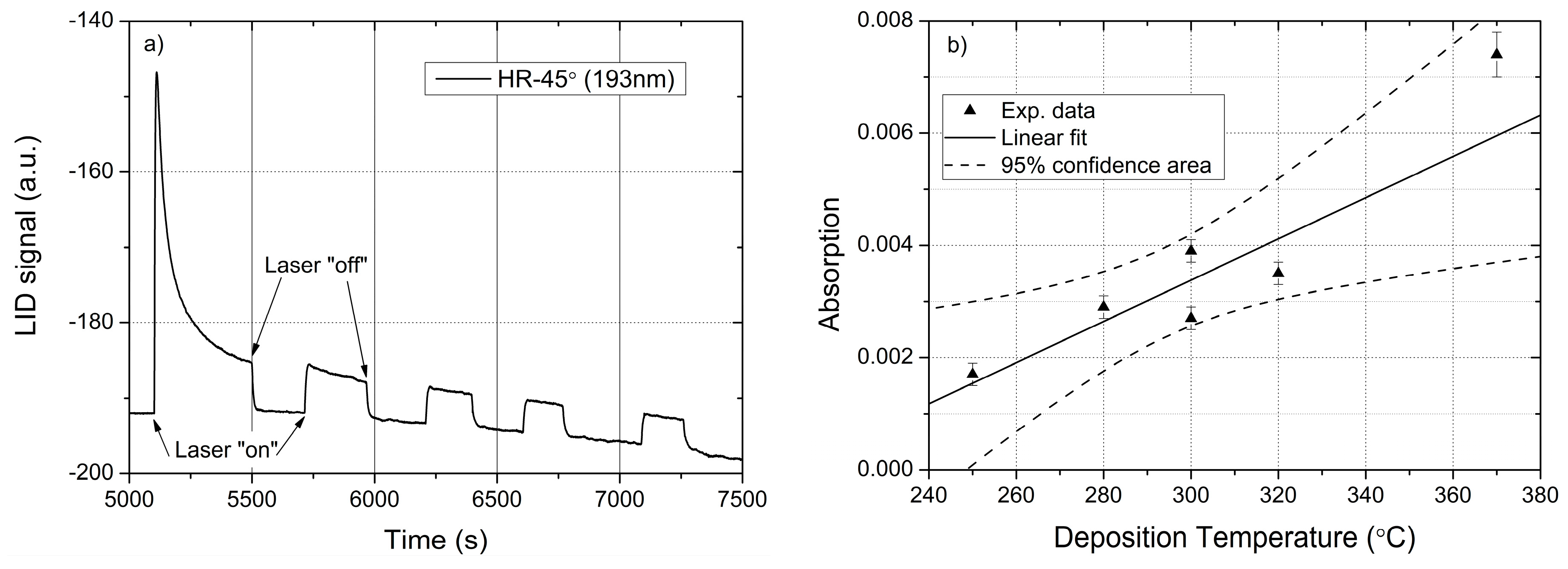
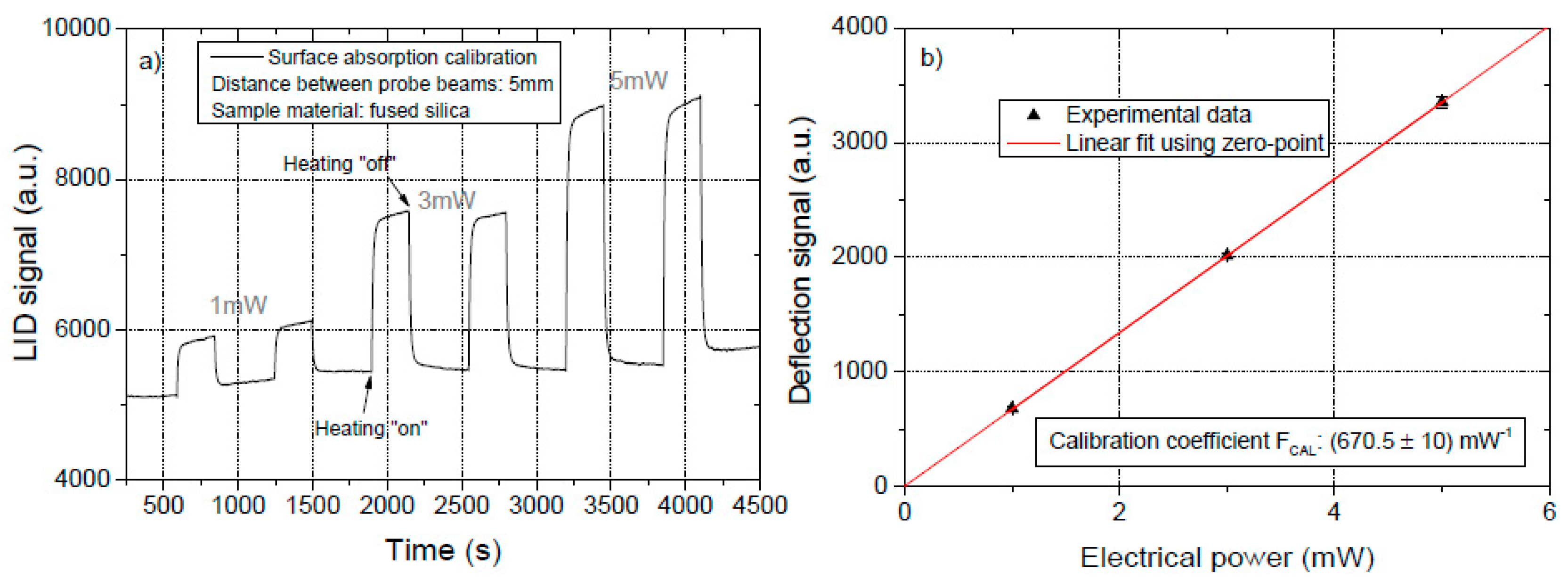
The calibration procedure itself is composed of measuring the probe beam deflection as a function of the electric power (
Figure 3a). Plotting the deflection signals versus electrical power gives a linear function (
Figure 3b) which spans over several orders of magnitude for the electric power [
8].
The calibration coefficient
FCAL is defined by the slope of the linear function including the zero-point, i.e., no electrical power means no probe beam deflection. It is valid for the applied combination of sample material and geometry. The unique feature and key advantage of this electric heating approach is the ability to calibrate the measurement setup without knowledge of the thermo-optical parameters of the sample. To verify the calibration procedure, separate reflectance, transmission, absorption and scattering measurements have been performed for different materials and coatings to proof the energy balance. The results have confirmed that within measurement accuracy, a value of 1 has been obtained for the energy balance in each of the investigations [
9].
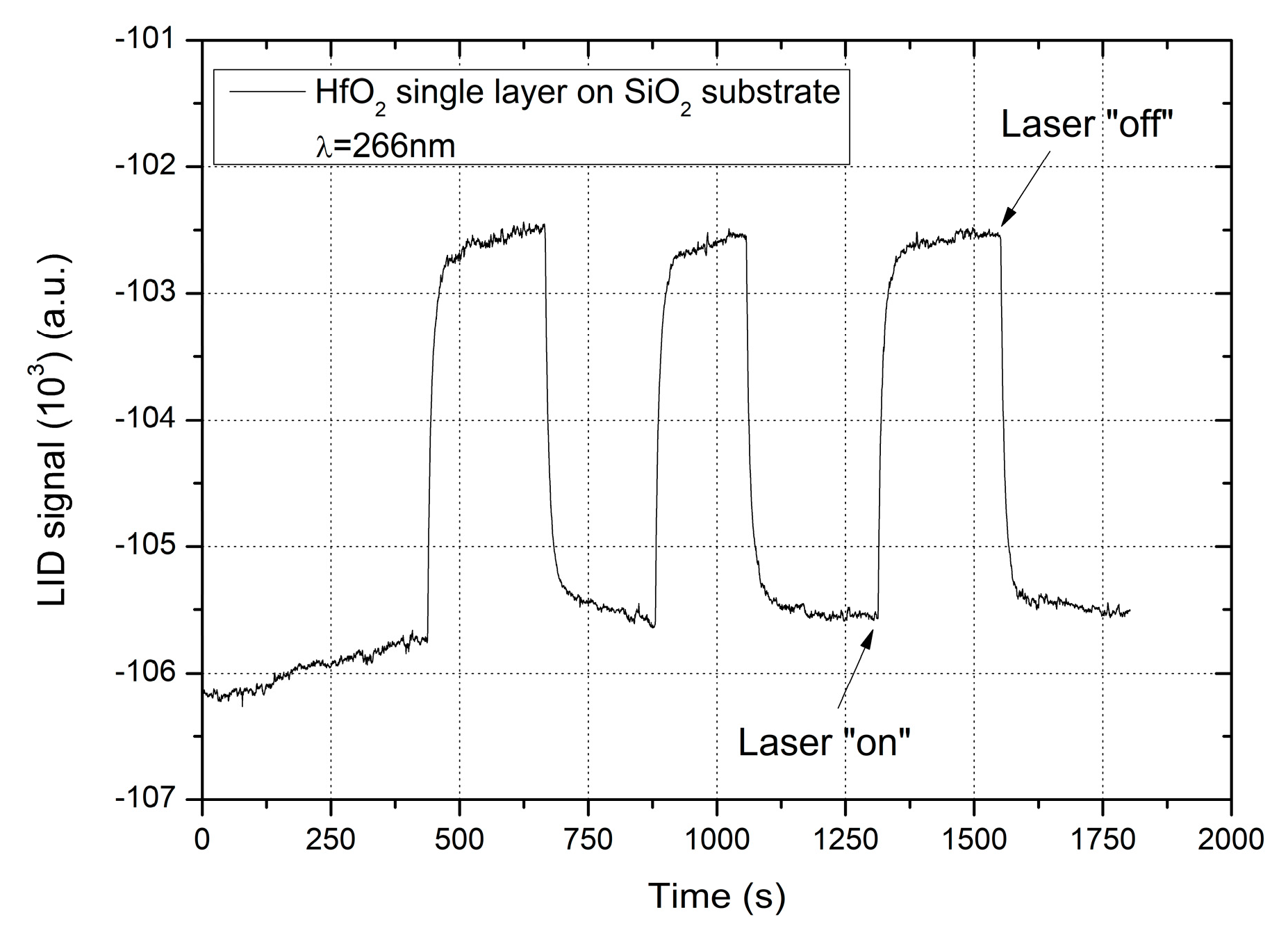
After completing the electrical calibration, the sample(s) of investigation are characterized.
Figure 4 gives a measurement example for an HfO
2 single layer upon 266 nm laser irradiation.
The measurement consists of three individual cycles comprising of the time between laser irradiation “on” and “off” events. Before the first cycle of the sample irradiation starts, the “base line” of the LID signal needs to be constant or show a constant drift (
Figure 4). This drift behavior is due to environmental changes like temperature in the setup surroundings. Small temperature variations already affect optic mountings within the setup by thermal expansion. As a result, small changes in the probe beam path and thus its location on the position sensitive detectors are detected.
Constant drifts during a measurement cycle are taken into account during data analysis. Here, the LID deflection signal is defined as the difference between the “base line” signal and the steady-state signal for the constant thermal lens upon irradiation. Once the LID deflection signals for all measurement cycles are obtained, their mean value is defined as the LID intensity ILID. Together with the corresponding mean pump laser power PL for all cycles and the calibration coefficient FCAL, the coating absorption A is calculated by
2.3. LID Measurement Concepts
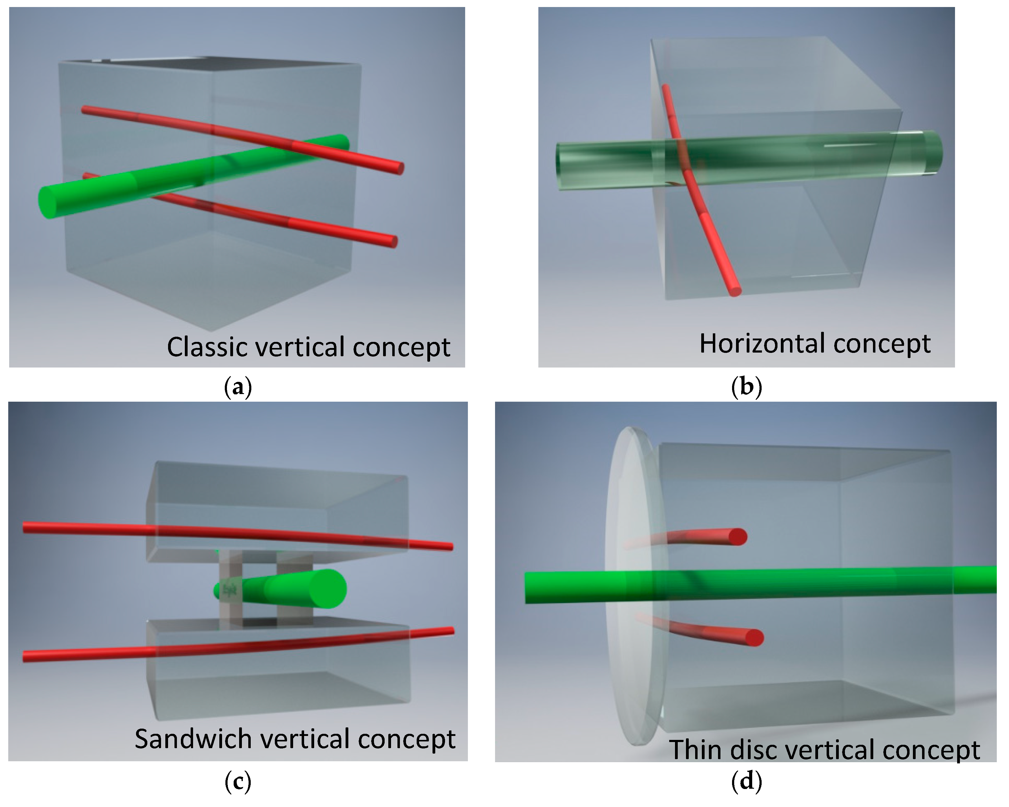
In order to account for the variety of measurement tasks, different concepts based on the LID technique have been developed (
Figure 5). For the different concepts, it was investigated whether to pass two probe beams through the sample outside the irradiated area or just one probe beam inside the irradiated area. Further, the two-dimensional PSD allows detecting both, the probe beam deflection in direction of the pump laser (= horizontal) or perpendicular to it (= vertical). Due to the general scheme in
Figure 1 it was tested how the LID technique can be adapted to round sample geometries without side-face polishing, which is a preferred geometry in coating manufacturing. Finally, particular attention is paid to increasing the sensitivity of substrates that are disadvantageous for photo-thermal measurements (e.g., Sapphire, CaF
2…). However, all the different concepts have been considered with respect to maintaining the electrical calibration procedure.
2.3.1. Classic Vertical Concept
The classic vertical concept (
Figure 5a) applies two probe beams above/beneath the irradiated spot and utilizes the probe beam deflection perpendicular to the pump beam direction. A high signal-to-noise ratio makes the vertical concept the best option for absorption measurements in bulk and highly reflective coatings if the required sample geometry can be supplied. The position of the probe beam can be changed with respect to the sample length. Consequently, for measuring coatings the probe beams pass the sample close to the coated surface while for bulk absorption measurement the probe beams pass the sample in the middle of the sample length where influences of the front/rear surfaces are minimal. In the case of transparent coatings, the deflection always comprises of both, the coating and substrate absorption. For separation, there are two approaches. For the first, an uncoated reference substrate of same geometry/material is measured additionally, and the difference in the deflection signals is assigned to the coating absorption. In case of double-side coated surfaces, however, only the sum of both coating absorptions is accessible. In order to avoid systematic errors, it is essential that the coated and uncoated substrates feature identical bulk and surface absorption properties. For a second approach, the deflection signals are measured at different positions along the sample length. In case of a single-side coated sample (neglecting the absorption of the uncoated surface), two different positions are required. Together with the corresponding bulk and surface absorption calibrations, the bulk and coating absorptions can be calculated. In contrast to the first approach, the individual coating absorptions of a double-side coated substrate are detectable by using three different measurement positions along the sample length.
2.3.2. Horizontal Concept
The only concept that breaks with the general LID scheme is the horizontal concept for coating measurements only. Here, in contrast, only one probe beam is guided centrally through the middle of the irradiated area at a position closest to the coated sample surface (
Figure 5b). The resulting deflection in the direction of the pump beam allows for detecting the surface absorption virtually free of the sample’s bulk absorption [
9]. Therefore, the horizontal concept is an alternative choice in particular for investigating anti-reflecting or partially reflecting coatings, where typically both bulk and coating absorption are present in the measurement signal for the classic vertical concept. Using only one probe beam instead of two reduces the signal-to-noise ratio compared to the classic vertical concept. However, no separation between bulk and coating absorption is required which yields an overall improvement for the measurement accuracy. A limitation for absolute absorption measurements is given by guiding the probe beam through the pump laser volume. The use of the electrical calibration now requires virtually identical areas for electrical and laser heating. This limits the concept to top-hat shaped pump laser beams.
2.3.3. Sandwich Vertical Concept
The sensitivity of photo-thermal absorption measurement techniques depends on the thermo-optical properties of the investigated material. For a variety of interesting materials, e.g., crystals like Sapphire or CaF2, this results in very small thermal lenses. While this is favorable in the application, the measurement sensitivity easily gets insufficient for very low absorption detection.
The recently demonstrated sandwich vertical concept (
Figure 5c) solves this issue [
10]. The basic principle consists of a small sample of investigation that is placed between two larger tiles of an appropriate optical material (→ sandwich). The pump laser still hits the sample of investigation and generates the absorption induced heat. The probe beams, however, are passing the sandwich tiles instead of the sample. The probe beams are now deflected by the thermal lens that is generated in the optical tiles after the absorption induced heat in the sample is transferred into the tiles.
There are a few prominent features related to this concept. Compared to the LID vertical concept, it enables a strong increase in measurement sensitivity for materials with a low photo-thermal response by choosing appropriate optical tile materials, e.g., fused silica [
10]. The reason is that now the probe beams use the thermo-optical properties of the sandwich tile material instead of those of the sample material. Strictly speaking, the low sensitivity materials like Sapphire or CaF
2 are now measured with the sensitivity for fused silica. Separating the sites of pump beam absorption (sample of investigation) and probe beam deflection (optical tiles) allows a sensitivity increase for many optical materials by more than an order of magnitude.
Apart from the sensitivity increase, the Sandwich vertical concept also overcomes another drawback of the LID technique. As a result of the transversal pump-probe configuration, not only two, but in total four polished side-faces are required in order to allow both pump and probe beam guiding through the sample. Recently, it was proven by electrical calibration and real measurements that the amount of heat transferred into the optical tiles until stationary thermal lens condition is the same whether the contact surfaces are polished or not [
11]. Therefore, the requirement for additional side-face polishing is omitted. Moreover, the investigated material does not need to be transparent for the probe beam anymore. This clears the way for potential investigations of infrared optical materials or metallic substrates.
2.3.4. Thin Disc Vertical Concept
Commonly in optical coating manufacturing, round shaped substrates are standard for thin film investigations. In particular, substrates of 1” diameter and 1mm thickness are used as reference samples for post-coating characterizations. In order to match this geometry to the LID concept, the thin disc vertical concept has been developed (
Figure 5d). Using a particularly designed holder, a thin round sample (1–2” diameter, thickness: 1–2 mm) is pressed against a rectangular (cubic) substrate. The latter possesses at least four polished side-faces to allow for a measurement similar to the classic vertical concept. Similar to the Sandwich vertical concept, the probe beams are guided through the rectangular substrate—instead of using the actual sample of investigation—and use the thermal lens that is generated by heat conduction from the absorption in the coated thin sample. For transparent coating investigations, the LID measuring signal is composed of three absorptions originating from the coating itself, the thin round sample substrate and the rectangular substrate. To identify the coating absorption, it is required to perform a reference measurement using an uncoated thin substrate of same geometry/material attached to the rectangular substrate. In case of double-side coated surfaces, however, only the sum of both coating absorptions is accessible. It is essential that the thin substrates feature identical bulk and surface absorption properties in order to avoid systematic errors.
3. Results and Discussion
This section contains a variety of experimental results in order to show the benefit of using direct absorption measurements for optical coating characterization. The scope ranges from influences of deposition parameters or impurities to laser irradiation induced effect, nonlinear absorption and separation between thin film and interface absorption.
3.1. Absorption vs. Coating Deposition Temperature (Thin Disc Vertical Concept)
One of the critical parameters in optical coating manufacturing is the deposition temperature. It has, for example, an impact on the thin film structure (→ refractive index, scattering) or the stoichiometry (→ defects). Nonstoichiometric films often give rise to increased absorption due to the formation of intrinsic defects. For oxide coatings these are preferable oxygen vacancies [
12,
13,
14] whereas for fluorides the formation of color centers or even localized metallic clusters is critical [
15,
16]. For our studies, high-reflecting (HR) mirrors (MgF
2/LaF
3) for 193 nm and AOI = 45° have been deposited onto CaF
2 substrates (1” diameter, thickness 2 mm) by thermal evaporation using deposition temperatures in the range 250–370 °C. Absorption measurements have been carried out by means of the thin disc vertical concept using an ArF excimer laser (ExciStar S Industrial, Coherent GmbH, Goettingen, Germany) with a repetition rate
f = 1 kHz. Upon laser irradiation, all samples showed an initial absorption decrease related to laser induced desorption of hydrocarbons (
Figure 6a) [
17].
Figure 6b displays the absorption data after initial decrease as function of the deposition temperature. The data show a linear increase in the HR coating absorption with deposition temperature.
However, it cannot be distinguished whether both materials contribute to the raising absorption. The finding of an absorption increase is somewhat unexpected, since often higher temperature (annealing) yields absorption improvement in optical thin films like LaF
3 [
19]. However, interface or structural properties (layer growth) may strongly depend on the deposition process and temperature and affect the overall absorption. Further, temperature related changes may be advantageous or disadvantageous, respectively, for the individual coating materials.
3.2. Absorption vs. Impurities (Thin Disc Vertical Concept)
Besides intrinsic defects, impurities play a large role for the absorption properties of optical coatings. However, they are caused by other sources like insufficiently pure raw materials or inner parts of the deposition chamber, e.g., crucibles. We compared different HfO
2 single layers (optical thickness: 4λ/4 @266 nm) on fused silica substrates (1” diameter, thickness 1mm), made by ion-assisted deposition (IAD) from different raw materials. Since HfO
2 is the most preferred high-index material in the UV range, we tested the absorption at the prominent laser wavelengths 355 nm (Spruce-355/5, Huaray Precision Lasers, Wuhan, China) and 266 nm (NANIO 266-2-V-development, InnoLas Photonics GmbH, Krailling, Germany), respectively. All thin films have been characterized by TOF-SIMS analysis. It was found, that in particular the iron content strongly varies amongst the raw materials.
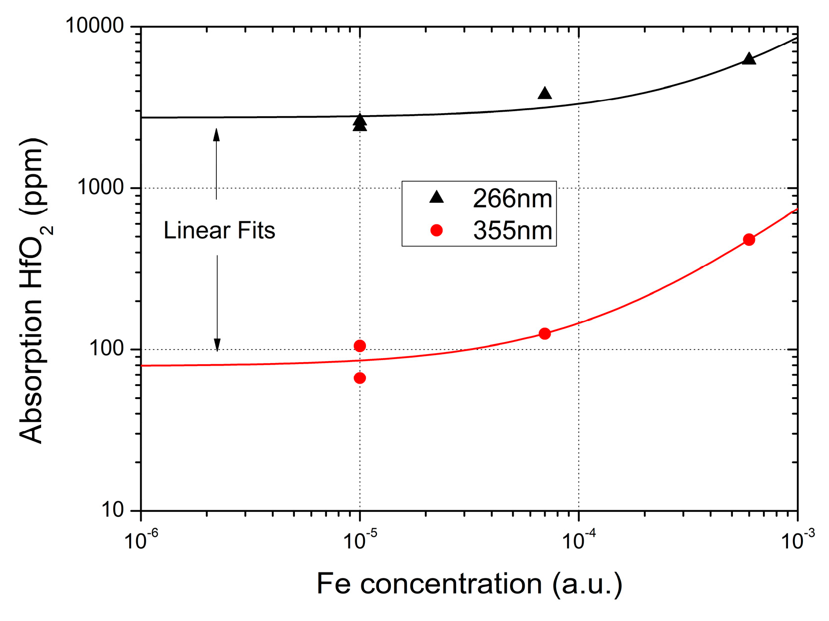
Figure 7 shows the HfO
2 layer absorption as a function of the iron content. It is seen that the HfO
2 absorption at 355 nm is significantly lower than at 266 nm which is attributed to the cumulative influence of the HfO
2 band edge. For both wavelengths, the absorption increases linearly with the iron concentration which coincides with the common very broad absorption bands of metallic impurities.
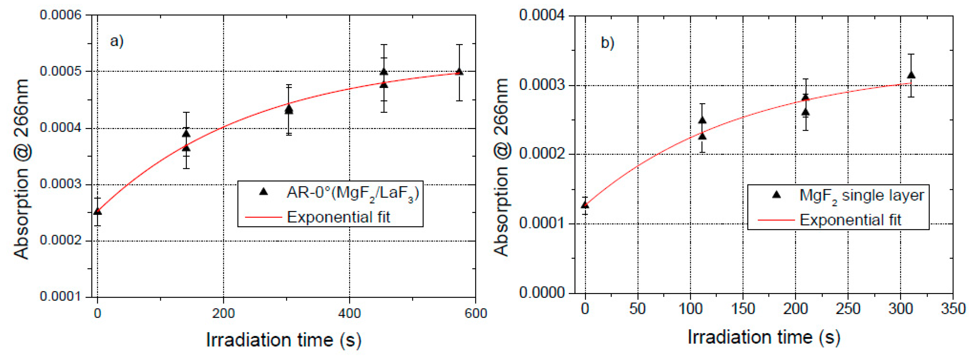
3.3. Absorption Change upon Initial Laser Irradiation (Thin Disc Vertical + Sandwich Concept)
Providing invariant laser operation requires optical components that do not alter upon laser irradiation. However, it is well-known that under exposure to UV or DUV laser light, even intrinsic defects in highly transparent optical materials can alter. A prominent example is fused silica where defect generation, defect annealing and defect transformation can occur upon initial ArF laser irradiation [
20]. Hence it is worth looking to the absorption properties of optical coatings with respect to their changes under intense UV or DUV laser irradiation. An AR coating based on MgF
2/LaF
3 has been deposited by thermal evaporation onto a CaF
2 substrate (1” diameter, thickness 1 mm). In addition, each of the coating materials has been deposited individually on separate substrates within the coating runs. The CaF
2 substrates have been attached to a fused silica cube for measurement (see
Figure 5d). Combining the thin vertical concept with the idea of the sandwich concept allows for a strong sensitivity increase (~factor of 10) by using the photo-thermal properties of fused silica instead of CaF
2. The three samples (AR, LaF
3, and MgF
2) have been irradiated at 266 nm (NANIO 266-2-V-development, InnoLas Photonics GmbH) with intermediate absorption measurements.
Figure 8a shows that during 10 minutes of laser irradiation, the absorption of the AR coating roughly has doubled before reaching a stationary value. The results of the individual coating materials give proof that while the LaF
3 thin film does not show any irradiation induced absorption change, the MgF
2 thin film nearly tripled its absorption during initial irradiation (
Figure 8b).
3.4. Separation between Thin Film and Interface Absorption (Thin Disc Vertical + Sandwich Concept)
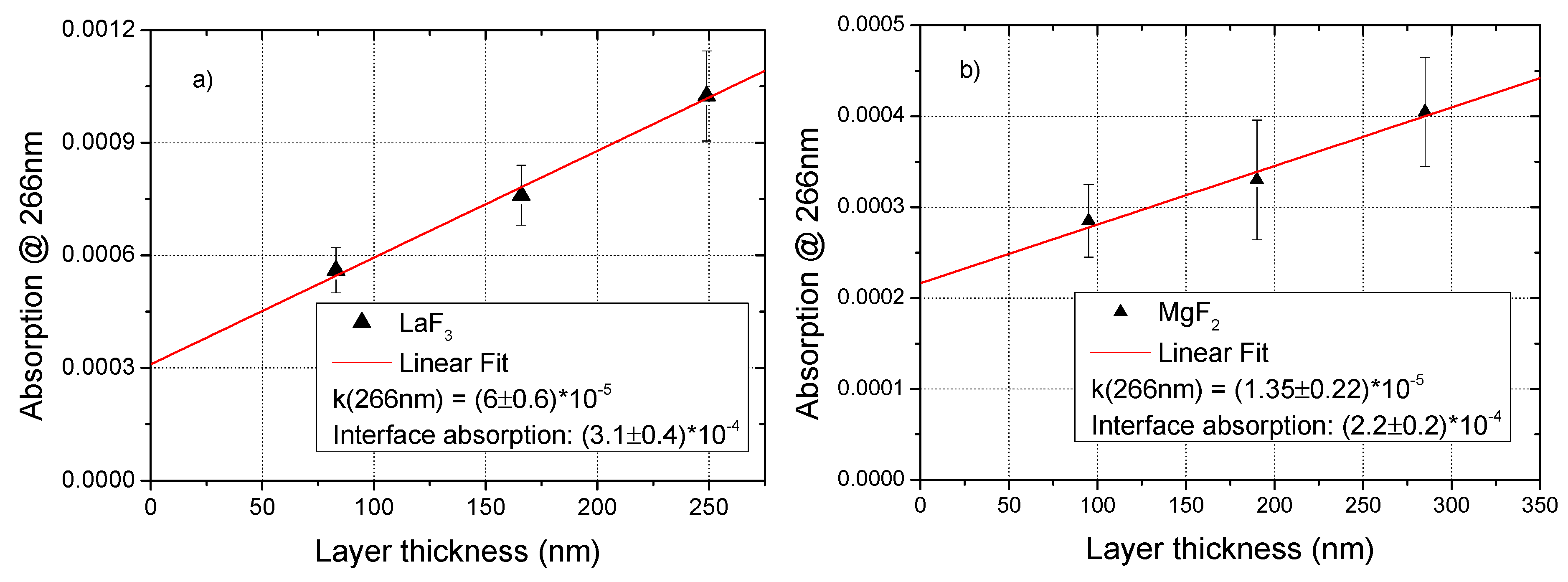
For transparent optical thin films like AR coatings, interface engineering i.e., surface polishing and cleaning, is the key to low absorption and corresponding to high resistance against very intense laser irradiation (LID—laser induced damage threshold). Inadequate surface preparation before the coating process may result in surface absorption not caused by the thin film itself. Consequently, strongly varying interface/surface absorption is likely to occur by different polishing/cleaning/coating technologies. Further, in order to simulate a total absorption of HR coatings, the absorption of the individual layer materials is required without contributions related to the substrate surface. Hence, separating between interface and thin film absorption by appropriate experiment design is highly required. One way to solve that issue is measuring a series of samples with different optical film thicknesses but identical surface preparation.
Figure 9 gives the results for LID absorption measurements at 266 nm (NANIO 266-2-V-development, InnoLas Photonics GmbH, Krailling, Germany) of single MgF
2 and LaF
3 single layers (thermal evaporation) on CaF2 substrates (1” diameter, thickness 1 mm) which have been attached to a fused silica cube for sensitivity enhancement.
The different layer thicknesses are matched to allow for optical thickness of multiple of λ/4 in order to generate identical surface reflectance. The results in
Figure 9 prove that the interface absorption contributes significantly to the total surface absorption. In particular for the thinnest layer of λ/4 thickness, the interface contribution can reach up to 50% and higher of the overall absorption. Consequently, the simulation for an HR mirror based on the investigated MgF
2 and LaF
3 materials would considerably overestimate its absorption and underestimate the achievable reflectivity. The
k values, calculated by
with α being the absorption coefficient per Nanometer and λ the wavelength, are in the 10
−5 range. These are reasonable data compared to commonly published data for the deep UV range [
15,
21].
3.5. Nonlinear Thin Film Absorption (Horizontal Concept)
For high laser intensities and/or short laser wavelengths, not only the linear but also a potential nonlinear absorption in the coatings need to be considered.
In the case of bulk materials, optical materials like SiO
2 or metal fluorides show very small intrinsic absorption due to their large bandgaps. High laser intensities, however, enables intrinsic or defect related nonlinear absorption, which is not accessible to common transmission measurements using spectrophotometers. Consequently, direct absorption measurement techniques combined with intense laser light have been applied to investigate the nonlinear absorption behavior in DUV bulk materials, mainly at the wavelengths 193, 248 and 266 nm. In contrast, very few experimental results exist with respect to the nonlinear absorption of the common thin film materials for the DUV wavelength region. This might originate from the linear absorption coefficients of coatings, which are significantly higher than for the corresponding bulk materials. Typically, any optical coating of a thickness of 10 mm would be completely opaque. Therefore, small nonlinear absorption might be hidden by a strong linear absorption background. However, recent experiments using direct absorption measurements have revealed measurable nonlinear absorption even in thin single layers [
22,
23,
24]. Similar to the linear absorption, it was demonstrated that two-photon absorption (TPA) coefficients in optical coatings remarkably exceed those for the corresponding bulk materials. To a certain extent, these enlarged nonlinear absorption values are referred to sequential two-step absorption processes via intermediate defect energy levels [
22].
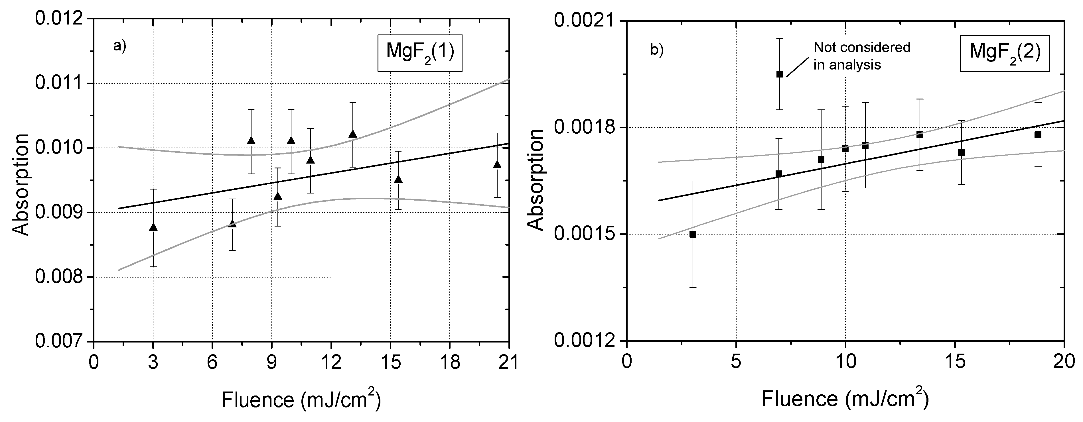
For investigating nonlinear absorption properties, two different MgF
2 thin films (thermal evaporation,
Table 1) on CaF
2 substrates (15 × 15 × 10 mm
3) have been measured at 193nm (ExciStar S Industrial, Coherent GmbH, Goettingen, Germany) as a function of the laser intensity. For very weak absorption values, i.e., α
h ≪ 1 and β
I0h ≪ 1, the light absorption
A in a thin film of a thickness
h as a function of the incident laser intensity
I0 can be simplified to
where α and β denote the one- and two-photon absorption coefficient, respectively. Therefore, using Equation (3) for the results of thin film absorption measurements as function of the laser intensity (or fluence) allow for a calculation of the two-photon absorption coefficient β.
Figure 10 shows the results for the two MgF
2 thin films.
Table 1 summarizes the calculated extinction coefficients and two-photon absorption coefficients for the investigated MgF
2 thin films. The
k values in the low to medium 10–4 range are very comparable to extinction coefficients obtained recently by spectral reflectance and transmission measurements [
15,
16,
21,
26,
27]. As in recently published investigations, the obtained two-photon absorption coefficients in this work are several orders of magnitude higher than those obtained for fluoride single crystals [
28,
29,
30,
31]. This might be explained in two ways. First, due to the typically low crystalline order of the thin films, their bandgaps are supposed to be lower than for the corresponding single crystal which can result in a higher nonlinear absorption coefficient. Second, a larger number of real defect states (extrinsic or intrinsic nature) are responsible for the high single photon absorption coefficient in thin films compared to the single crystals. Therefore, bridging the bandgap is likely to occur by sequential two-step absorption using intermediate defect energy levels. For such a scenario, the defect related, effective two-photon absorption can substantially exceed the intrinsic two-photon absorption via virtual energy states [
31].
4. Summary and Outlook
We have demonstrated that the combination of photo-thermal absorption measurement and reliable absolute calibration via electrical heaters allow for enhanced characterization of optical coatings. Based on the general idea of the laser induced deflection (LID) technique, a variety of concepts have been derived and presented to allow for different measurement requirements. Here, particular attention has been paid to realize the measurement of round sample geometries commonly used in coating characterization. Further, measuring transparent optical coatings with negligible contribution from the underlying substrate has been demonstrated. Finally, a concept is depicted to overcome the drawback of photo-thermally insensitive substrate materials like CaF2 or Sapphire.
Reliable absolute calibration is one of the most important issues for photo-thermal absorption measurements. In contrast to common simulation procedures or use of samples with known absorption properties, an electrical calibration adapted from the calorimetric absorption measurement is applied. Hereby, an absolute calibration of the setup is carried out without any knowledge of the substrate’s material parameters. However, it is required to use a calibration substrate of same geometry and material as the sample of investigation.
Experimental results have been presented for prominent UV and deep UV laser wavelengths (355, 266 and 193 nm), covering a variety of factors that critically can influence the absorption properties in optical coatings e.g., the deposition process, defects and impurities, intense laser irradiation and surface/interface engineering. The UV and deep UV wavelength region has been chosen because here, the combination of high laser intensity and high photon energy gives rise to enhanced interaction between the laser light and the optical coating. Further, prominent absorption bands of defects and impurities are located in the considered spectral region, e.g., color centers or oxygen deficiency centers.
With respect to round substrate geometries, current activities are ongoing to adapt the LID technique also to thick round standard substrates (e.g., thickness ¼”). Applying the thin round vertical concept would result in too low a sensitivity due to the large distance between the coating and the probe beams. The thick substrates are in particular applied for mirrors of highest reflectance (>99.99%). The ability to use the LID technique would give an additional advantage to optical coating characterization in combination with the cavity ring-down (CRD) technique that is used to precisely determine the mirror’s reflectance. Thereby it would be possible to separate between absorption and scattering loss contributions allowing a defined improvement of highly reflecting mirrors.
Author Contributions
Conceptualization, C.M.; Validation, S.B. and C.M.; Formal Analysis, S.B. and C.M.; Investigation, S.B and C.M; Data Curation, C.M.; Writing—Original Draft Preparation, C.M.; Writing—Review and Editing, S.B.; Visualization, C.M.; Supervision, C.M.; Project Administration, C.M.; Funding Acquisition, C.M.
Funding
This research was funded by GERMAN FEDERAL MINISTRY OF ECONOMICS AND TECHNOLOGY within the framework of the Confederation of Industrial Research Associations, grant numbers KF2206909UW2 and ZF4006807RE5.
Acknowledgments
The authors are grateful to company Layertec GmbH for providing the majority of the coated samples as well as for the TOF-SIMS investigations.
Conflicts of Interest
The authors declare no conflict of interest.
References
- Li, B.; Blaschke, H.; Ristau, D. Combined laser calorimetry and photothermal technique for absorption measurement of optical coatings. Appl. Opt. 2006, 45, 5827–5831. [Google Scholar] [CrossRef] [PubMed]
- Leonid, S. Light-induced absorption in materials studied by photothermal methods. Recent Pat. Eng. 2009, 3, 129–145. [Google Scholar] [CrossRef]
- Alexandrovski, A.; Fejer, M.; Markosian, A.; Route, R. Photothermal common-path interferometry (PCI): New developments. Proc. SPIE 2009, 7193, 71930D. [Google Scholar]
- Yoshida, S.; Reitze, D.H.; Tanner, D.B.; Mansell, J.D. Method for measuring small optical absorption coefficients with use of a Shack–Hartmann wave-front detector. Appl. Opt. 2003, 42, 4835–4840. [Google Scholar] [CrossRef] [PubMed]
- Waasem, N.; Fieberg, S.; Hauser, J.; Gomes, G.; Haertle, D.; Kühnemann, F.; Buse, K. Photoacustic absorption spectrometer for highly transparent dielectrics with parts-per-million sensitivity. Rev. Sci. Instrum. 2013, 84, 23109. [Google Scholar] [CrossRef] [PubMed]
- Guntau, M.; Triebel, W. A Novel method to measure bulk absorption in optically transparent materials. Rev. Sci. Instr. 2000, 71, 2279–2282. [Google Scholar] [CrossRef]
- Mühlig, C.; Triebel, W.; Kufert, S.; Bublitz, S. Characterization of low losses in optical thin films and materials. Appl. Opt. 2008, 47, C135–C142. [Google Scholar] [CrossRef]
- Mühlig, C.; Kufert, S.; Bublitz, S.; Speck, U. Laser induced deflection technique for absolute thin film absorption measurement: Optimized concepts and experimental results. Appl. Opt. 2011, 50, C449–C456. [Google Scholar] [CrossRef]
- Mühlig, C.; Bublitz, S. Sensitive and absolute absorption measurements in optical materials and coatings by laser induced deflection (LID) technique. Opt. Eng. 2012, 51, 121812. [Google Scholar] [CrossRef]
- Mühlig, C.; Bublitz, S.; Paa, W. Enhanced laser-induced deflection measurements for low absorbing highly reflecting mirrors. Appl. Opt. 2014, 53, A16–A20. [Google Scholar] [CrossRef]
- Mühlig, C.; Bublitz, S.; Paa, W. Sandwich concept: Enhancement for direct absorption measurements by laser induced deflection (LID) technique. In Proceedings of the Laser-Induced Damage in Optical Materials, Boulder, CO, USA, 23–26 September 2012. [Google Scholar]
- Heber, J.; Mühlig, C.; Triebel, W.; Danz, N.; Thielsch, R.; Kaiser, N. Deep UV laser induced luminescence in oxide thin films. Appl. Phys. A 2002, 75, 637–640. [Google Scholar] [CrossRef]
- Papernov, S.; Brunsman, M.D.; Oliver, J.B.; Hoffman, B.N.; Kozlov, A.A.; Demos, S.G.; Shvydky, A.; Cavalcante, F.H.; Yang, L.; Menoni, C.S.; et al. Optical properties of oxygen vacancies in HfO2 thin films studied by absorption and luminescence spectroscopy. Opt. Exp. 2018, 26, 17608–17623. [Google Scholar] [CrossRef] [PubMed]
- Ivanova, E.V.; Zamoryanskaya, M.V.; Rustovarov, V.A.; Aliev, V.S.; Gritsenko, V.A.; Yelisseyev, A.P. Cathodo-and photoluminescence increase in amorphous hafnium oxide under annealing in oxygen. J. Exp. Theor. Phys. 2015, 120, 710–715. [Google Scholar] [CrossRef]
- Dumas, L.; Quesnel, E.; Pierre, F.; Bertin, F. Optical properties of magnesium fluoride thin films produced by argon ion-beam assisted deposition. J. Vac. Sci. Technol. A 2002, 20, 102–106. [Google Scholar] [CrossRef]
- Larruquert, J.I.; Keski-Kuha, R.A.M. Far ultraviolet optical properties of MgF2 films deposited by ion-beam sputtering and their application as protective coatings for Al. Opt. Commun. 2003, 215, 93–99. [Google Scholar] [CrossRef]
- Heber, J.; Mühlig, C.; Triebel, W.; Danz, N.; Thielsch, R.; Kaiser, N. Deep UV laser induced luminescence in fluoride thin films. Appl. Phys. A 2003, 76, 123–128. [Google Scholar] [CrossRef]
- Mühlig, C.; Triebel, W.; Kufert, S.; Bublitz, S. Laser induced fluorescence and absorption measurements for DUV optical thin film characterization. In Proceedings of the Advances in Optical Thin Films III, Scotland, UK, 2–5 September 2008. [Google Scholar]
- Mühlig, C. Absorption and fluorescence measurements in optical coatings. In Optical Characterization of Thin Solid Films, 1st ed.; Stenzel, O., Ohlidal, M., Eds.; Springer International Publishing AG: Cham, Switzerland, 2018; Volume 64, pp. 407–432. [Google Scholar]
- Mühlig, C.; Stafast, H.; Triebel, W. Generation and annealing of defects in virgin fused silica (type III) upon ArF laser irradiation: Transmission measurements and kinetic model. J. Non-Cryst. Solids 2008, 354, 25–31. [Google Scholar] [CrossRef]
- Bischoff, M.; Gäbler, D.; Kaiser, N.; Chuvilin, A.; Kaiser, U.; Tünnermann, A. Optical and structural properties of LaF3 thin films. Appl. Opt. 2008, 47, C157–C161. [Google Scholar] [CrossRef]
- Apel, O.; Mann, K.; Zoellner, A.; Goetzelmann, R.; Eva, E. Nonlinear absorption of thin Al2O3 films at 193 nm. Appl. Opt. 2000, 39, 3165–3169. [Google Scholar] [CrossRef]
- Li, B.; Xiong, S.; Zhang, Y.; Martin, S.; Welsch, E. Nonlinear absorption measurement of UV dielectric components by pulsed top-hat beam thermal lens. Opt. Commun. 2005, 244, 367–376. [Google Scholar] [CrossRef]
- Jensen, L.; Mende, M.; Schrameyer, S.; Jupé, M.; Ristau, D. Role of two-photon absorption in Ta2O5 thin films in nanosecond laser-induced damage. Opt. Exp. 2012, 37, 4329–4331. [Google Scholar]
- Mühlig, C.; Bublitz, S.; Kufert, S. Nonlinear absorption in single LaF3 and MgF2 layers at 193 nm measured by surface sensitive laser induced deflection technique. Appl. Opt. 2009, 48, 6781–6787. [Google Scholar] [CrossRef] [PubMed]
- Taki, Y. Film structure and optical constants of magnetron-sputtered fluoridic films for deep ultraviolet lithography. Vacuum 2004, 74, 431–435. [Google Scholar] [CrossRef]
- Shuzhen, S.; Jianda, S.; Chunyan, L.; Kui, Y.; Zhengxiu, F.; Lei, C. High-reflectance 193 nm Al2O3/MgF2 mirrors. Appl. Surf. Sci. 2005, 249, 157–161. [Google Scholar] [CrossRef]
- Görling, C. Wechselwirkungsmechanismen Von DUV- und VUV-Laserstrahlung Mit Fluoridischen Einkristallen. Ph.D. Thesis, Georg-August-University, Gottingen, Germany, 2003. [Google Scholar]
- Taylor, A.J.; Gibson, R.B.; Roberts, J.P. Two-photon absorption at 248 nm in ultraviolet window materials. Opt. Lett. 1988, 13, 814–816. [Google Scholar] [CrossRef] [PubMed]
- Kittelmann, O.; Ringling, J. Intensity-dependent transmission properties of window materials at 193 nm irradiation. Opt. Lett. 1994, 19, 2053–2055. [Google Scholar] [CrossRef] [PubMed]
- Mühlig, C.; Triebel, W.; Stafast, H.; Letz, M. Influence of Na-related defects on ArF laser absorption in CaF2. Appl. Phys. B 2010, 99, 525–533. [Google Scholar] [CrossRef]
© 2019 by the authors. Licensee MDPI, Basel, Switzerland. This article is an open access article distributed under the terms and conditions of the Creative Commons Attribution (CC BY) license (http://creativecommons.org/licenses/by/4.0/).


