Article

Enhancement of Critical Current Density by Establishing a YBa2Cu3O7−x/LaAlO3/YBa2Cu3O7−x Quasi-Trilayer Architecture Using the Sol-Gel Method

1
College of Vanadium and Titanium, Panzhihua University, Panzhihua 617000, China
2
School of Biological and Chemical Engineering, Panzhihua University, Panzhihua 617000, China
*
Author to whom correspondence should be addressed.
Coatings 2019, 9(7), 437; https://doi.org/10.3390/coatings9070437
Submission received: 1 July 2019 / Revised: 8 July 2019 / Accepted: 10 July 2019 / Published: 13 July 2019
(This article belongs to the Special Issue Superconducting Films and Nanostructures)

Abstract

:
We developed a solution-derived method to establish a YBa2Cu3O7−x/LaAlO3/YBa2Cu3O7−x quasi-trilayer architecture. Using the method, nano-scale pinning sites were induced into the quasi-trilayer architecture and yielded an apparent improvement in the in-field critical current density (Jc) of high-quality YBa2Cu3O7−x (YBCO). The improvement in the in-field Jc of the films was closely related to the thickness of the LaAlO3 (LAO) interlayer. In this paper it is demonstrated that when the nominal interlayer thickness approximates 20 nm, which is slightly higher than the roughness of the YBa2Cu3O7−x surface, the LaAlO3 interlayer is discontinuous due to synchromesh-like growth of the LaAlO3 layer on relatively rough YBa2Cu3O7−x surface resulting from the mobility of the solution. Nanoscale defects, such as particles, some amorphous phases, and especially their concomitant lattice defects (such as stacking faults and plane buckling) arise in YBa2Cu3O7−x layers. These nanoscale defects could play a role in flux pinning and thus enhancing Jc. The effective non-vacuum solution to induce vortex pinning into YBa2Cu3O7−x films could be a reference for the further design of an optimal pinning landscape for higher Jc.

1. Introduction

YBa2Cu3O7−x (YBCO)-coated conductors with high current-carrying capacity at liquid nitrogen temperature are currently thought to be the best candidates for power application1 [1,2,3,4,5]. It is well known, however, that the critical current density (Jc) of YBCO-coated conductors or films decay exponentially with an applied magnetic field [6,7,8]. For practical application, enhancement of Jc in magnetic fields is urgently needed in order to produce higher-performance coated conductors or films. In YBCO films, grain boundaries and vortex pinning determine Jc. At 65–77 K, vortex pinning is more crucial to Jc [9,10,11,12,13]. In the last 20 years, there have been a large number of research studies on vortex pinning, and great progress has been made on Jc improvement, but the pinning mechanism is controversial and the pinning landscape is ill-defined. In fact, many thin-film defects, such as surface precipitates, twin boundaries, surface roughness or a-axis grains, misoriented grains and grain boundaries, point defects, planar defects, and voids, have been proposed as flux pinning sites in YBCO. Foltyn’s group observed that anything that locally disrupts crystalline perfection on a scale of 0.1–1.0 nm is a candidate [14]. The challenges in engineering defect structures for achieving the best performance are to determine which structures are beneficial and to tailor their density to produce the desired effects without obstructing the current. One of the most important and interesting issues is developing a novel way to produce a special defect type and investigating the effectiveness of defects for flux pinning.
There are a great number of ways to induce nanoscale film defects into YBCO as flux pinning sites, which can be divided into two categories. One is to design some defect structures on the substrate surface prior to YBCO film deposition, to form extended defects on YBCO films. The other is to directly add defects into YBCO films by doping or inserting another film between YBCO layers, which may produce several types of defects such as one-dimensional nanorods, nanodots, two-dimensional low angle boundaries, surface precipitation, and three-dimensional nano arrays [15,16,17,18]. For the latter, a previous study found that when an extra layer was inserted among YBCO layers, Jc variation was observed by altering the interlayer thickness [19]. Several investigators have inserted CeO2 [19,20,21], Y2O3 [22], SrTiO3 [23], and NdBa2Cu3O7−x [24] into YBCO layers through various vacuum deposition processes and obtained some interesting results. However, little research has been done on establishing a quasi-multilayer structure using the sol-gel method. During the sol-gel process, the fluidity of the precursor solution is likely to have a significant effect on the interface of the quasi-multilayer structure, which will further affect Jc greatly. To perfect the flux pinning mechanism for further enhancing the in-field Jc of YBCO conductors, an important goal is to develop new methods that can produce a special defect landscape and achieve the strongest pinning.
In this work, we established a YBCO/LaAlO3 (LAO)/YBCO trilayer or quasi-trilayer architecture, all using the sol-gel method. In the YBCO-based architecture, an LaAlO3 (LAO) layer with pseudo-cubic structure was chosen as the extra layer in order to increase the Jc of YBCO films. There are two main reasons for choosing LAO: (1) lattice matching between LAO and YBCO is beneficial for epitaxial growth, and (2) because phase transition of LAO at ~435 °C may cause stress or defects in a YBCO film, which may also pin vortices [18]. Indeed, the results demonstrated that an apparent improvement was achieved in the in-field Jc of high-quality YBCO by establishing a YBa2Cu3O7−x/LaAlO3/YBa2Cu3O7−x quasi-trilayer architecture using the sol-gel method. The cause for the improved Jc was generally considered to be that the inserted layer suppressed Jc decay with increasing film thickness because the inserted layer could improve the epitaxial feature of the films; however, here, we show that the inserted layer could also induce nanoscale defects into YBCO films, which behave as flux pinning sites.

2. Experiments

2.1. Film Preparation

The precursor solution of YBCO films was obtained by dissolving fluorine-contained yttrium, non-fluorine barium, and non-fluorine copper acetate salts into methanol with the help of acrylic acid [25,26]. The total metallic ion concentration of the synthesized precursor solution was 1.2 mol/L. Using the low-fluorine solution, the YBCO gel films were produced by dip coating on single-crystal LAO (001) substrate. The withdrawal speed was controlled at 1 mm/s for the bottom YBCO and 2 mm/s for the top YBCO. The dip-coated gel films were pyrolyzed at 450 °C for 15 min and then fired at 800 °C for 100 min. The mixture atmosphere of O2 and N2 was controlled by a precision mass flowmeter with an O2 content of 1.3%. During the heat treatments, an appropriate moisture level was necessary for the formation of the YBCO phase. The moisture was introduced by bubbling deionized water with a dew-point temperature of 40 °C. After firing, the films were oxygenated at 450 °C for 2 h, which transformed the YBCO into an orthogonal structure with superconducting properties.
To make the LAO precursor solution, lanthanum (III) nitrate hexahydrate and aluminium tri-sec-butoxide were dissolved into absolute ethyl alcohol using acetylacetone and propanetriol as additives. After stirring for 2 h, a clear LAO precursor solution was obtained. The concentration of the solution was 0.3 mol/L, which was achieved by altering the content of ethyl alcohol. The pH value of the LAO precursor solution was 7–8, which is moderate for dipping YBCO films. Otherwise, prefabricated bottom YBCO films would be significantly corroded in LAO solution with aluminium nitrate as an Al source (pH value of ~2), as used in our previous work [27].
Using an LAO precursor solution with a pH between 7–8, a uniform LAO gel film could be obtained on the YBCO-coated LAO substrate by a dip-coating process. The withdrawal speed was controlled at 1 mm/s. Subsequently, the LAO gel film was fired at 800 °C for 30 min in flowing N2 and 1.3 vol% O2 atmosphere, and an LAO film was formed. Film thickness was established by repeating the processes of dip-coating and firing. Finally, the top YBCO film was grown on an LAO/YBCO bilayer so that the YBCO/LAO/YBCO trilayer (or quasi-trilayer) architecture was formed entirely using the sol-gel method. The schematic diagram of the YBCO/LAO/YBCO trilayer architecture is shown in Figure 1. In this paper, YBCO/LAO/YBCO trilayer films with a nominal thickness of LAO interlayers of 20, 40, and 70 nm were obtained and named SIS-20, SIS-40, and SIS-70, respectively. For comparison, YBCO-YBCO films without any interlayers were prepared in the same batch with bottom and top YBCO layers during the fabrication of the YBCO/LAO/YBCO trilayer. The YBCO-YBCO films were named SS.

2.2. Film Testing

The thicknesses of all of the films were measured using a Surfcorder-SE3500 surface profiler (Kosaka, Japan). A 7000S-type X-ray diffractometer (XRD) (Shimadzu, Japan) was used to detect the phases and crystalline orientations of the as-prepared films. Scanning electron microscopy (SEM) experiments were performed on a JEM-6700F (JEOL, Tokyo, Japan). A JEM-3010-type (JEOL, Tokyo, Japan) transmission electron microscopy (TEM) was employed to observe the microstructure of the samples. An atomic force microscope (AFM) was conducted on YBCO film to evaluate the surface roughness. A VersaLab multi-function vibrating sample magnetometer (Quantum Design, San Diego, CA, USA) was used to measure the magnetic moment m under a varying magnetic field, then Jc was calculated using the extended Bean model, as given by Equation (1) [28,29]:
Jc = 20Δm/[Va(1 − a/3b)]
where Δm is the vertical width in the m-B loop in a certain field, and V, a, and b (a < b) are the volume, width, and length of the films, respectively. The size of the films used in the magnetization measurement was 2.5 × 3.0 mm. The temperature was fixed at 77 K, and a field with magnetic strength between 0–3 T was applied perpendicular to the film surface during measurements.

3. Results and Discussion

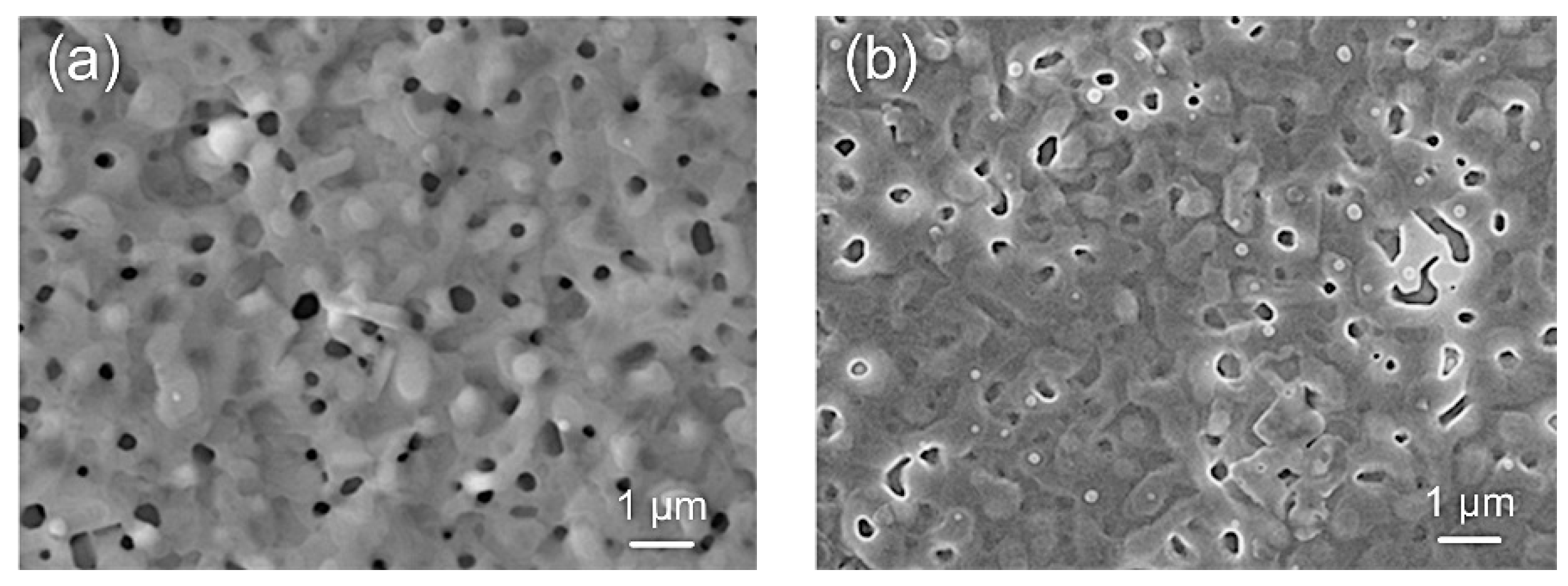
3.1. Jc of YBCO/LAO/YBCO Trilayer

Figure 2 shows typical M-H curves of YBCO/LAO/YBCO films with different LAO thicknesses measured at 77 K. As shown in this figure, the intensity of magnetization for samples SIS-40 and SIS-70 was low. Through calculating by the Bean model, it was found that Jc (self-field) was lower than 103 A/cm2, which is much lower than typical Jc values (106 A/cm2) of YBCO films [27]. During the process of building up the LAO thickness, the bottom YBCO film suffered from repeated heat treatments, which did not benefit the film orientation. However, when the thickness of the LAO interlayer was 20 nm, sample SIS-20 showed an enhanced magnetic intensity (M) compared with sample SS with the similar thickness of YBCO layer.
According to the M-H curves of samples SS and SIS-20, the Jc at 0–3 T was calculated, and the results are shown in Figure 3. From the figure, it is obvious that the Jc of SIS-20 was higher than that of SS under all measured fields. By comparison, the Jc of SIS-20 compared to that of SS was 2.5 times at 1 T, 2.8 times at 2 T, and 3.4 times at 3 T.
After firing the LAO film, 20 nm-thickness LAO layers were not enough to cover the entire bottom YBCO layer due to the rough surface of the solution-derived YBCO film, which will be shown below, leading to contact directly between the top and bottom YBCO layers. This means that the LAO is a discontinuous layer between YBCO layers. It is likely that a series of induced defects arise inside the quasi-trilayer, which contributes to flux pinning and increases Jc. The details are discussed below.

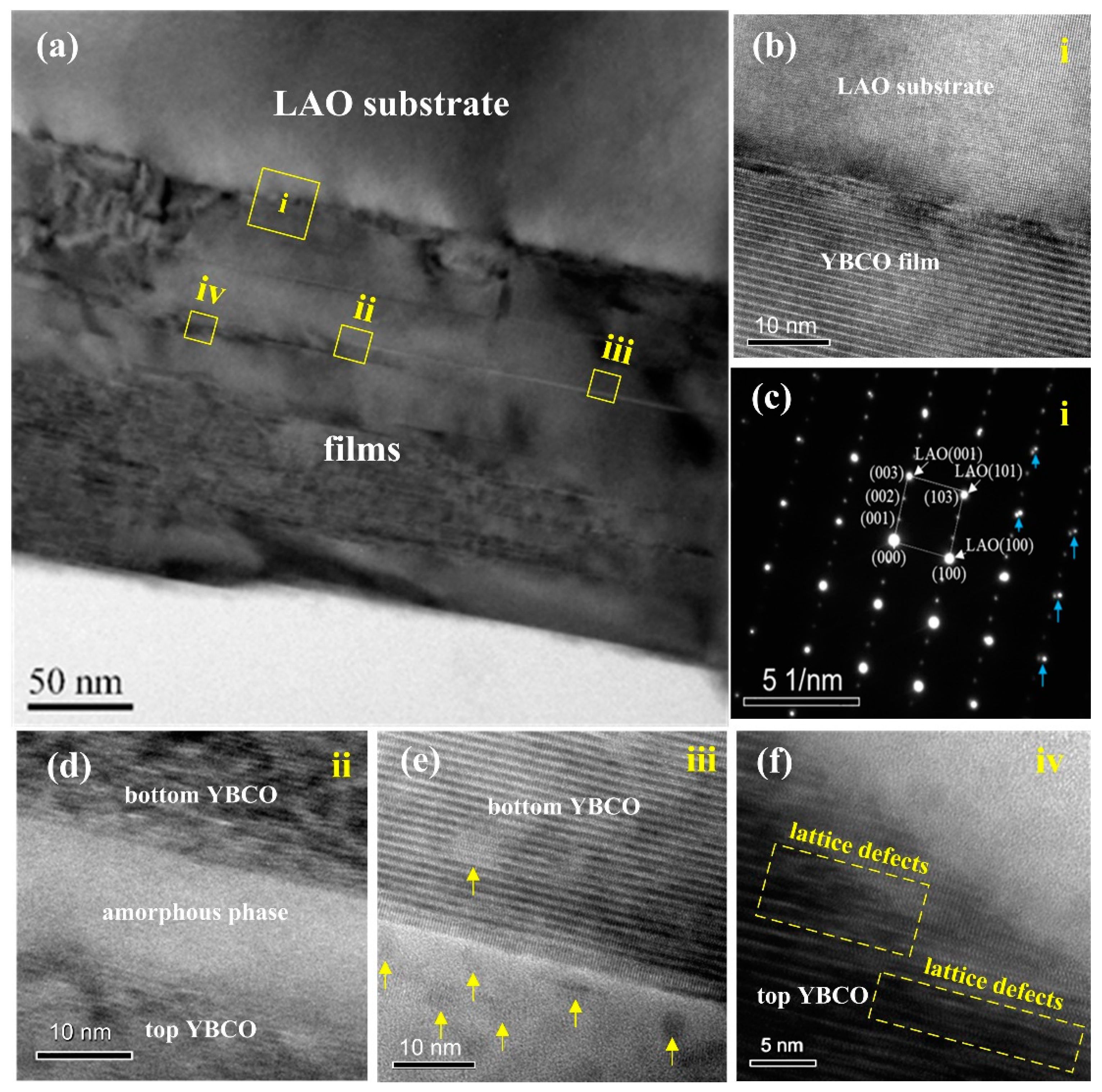
3.2. Mechanism of the Jc Variation

It was found that the interlayer thickness had a great influence on the Jc of the YBCO/LAO/YBCO trilayer, as shown in Figure 2. To further analyse the Jc variation in the trilayer, it is necessary to characterize the microstructure of the trilayer. In this part, we mainly investigate three aspects: phase and orientation, surface morphology, and high-resolution microstructure of the trilayer.
Figure 4 shows XRD patterns of the YBCO/LAO/YBCO trilayer with different LAO thicknesses. To distinguish weaker diffraction peaks, the ordinate was logarithmically processed. It can be seen from the figure that strong YBCO (00l) diffraction peaks appear in the four samples of SS, SIS-20, SIS-40, and SIS-70, indicating that the YBCO films have good c-axis preferred orientation. However, when the intermediate LAO layer is thick, in the SIS-70 sample, the diffraction peak at 2θ of 41.1° is identified as the (111) crystal plane of the LAO film, and the diffraction peak at 2θ of 32.8° s identified as the (103) crystal plane of the YBCO film. This indicates that non-c-axis oriented grains arose in sample SIS-70, which could reduce Jc dramatically. In the XRD patterns of SIS-40, SIS-20, and SS samples, there were no other peaks except the (00l) crystal plane of both YBCO and LAO, indicating that the sample had a good c-axis orientation when the intermediate LAO interlayer was thin.
The surfaces of the top YBCO layer of the four samples SS, SIS-20, SIS-40, and SIS-70 were observed, as shown in Figure 5. Since the lattice constant of YBCO in the c-axis direction is approximately three times longer than that in the a-axis (or b-axis) direction, usually the a- (b-) axis grains at the surface are needle-like or strip-shaped, while the c-axis grains are columnar through the film [8]. It can be seen from Figure 5 that although the SS sample had many holes on the surface, there were no needle-like or strip-shaped a-axis grains, and almost all of them were columnar c-axis grains. The columnar c-axis grains are advantageous for current transport in the ab plane of the YBCO film. The surface of the SIS-20 sample also exhibited a large amount of c-axis grains, but the surface was denser than the SS sample, which is beneficial for high Jc [26]. The surface of the SIS-40 sample was almost c-axis, but a small number of holes appeared; SIS-70 showed a large number of small particles, which would be likely to degrade Jc.
In combination with XRD analysis, it can be inferred that these large numbers of small particles in sample SIS-70 were induced by non-c-axis grains appearing in the LAO layer during the preparation of the intermediate LAO film, and these small particles are likely to have been YBCO (103)-oriented grains. As the thickness of the LAO interlayer increased, the subsequent growth of the top-layer YBCO film had a relatively poor c-axis orientation due to the deterioration of its own orientation (the occurrence of non-c-axis LAO (111) diffraction peaks in XRD). This trend was most prominent at the top surface of the YBCO film.
To further explore the reason for the enhanced Jc of the SIS-20 sample, the sample was subjected to transmission electron microscopic observation. Figure 6a is a TEM image of a YBCO/LAO/YBCO quasi-trilayer film (SIS-20 sample). As seen in the figure, the overall thickness of the film was approximately 180 nm. No continuous LAO layer was found in this range, indicating that the top and bottom YBCO layers were connected together in some area.
Amplification of the boxed areas i–iv in Figure 6a shows a high-resolution transmission electron microscopy image and the selected area electron diffraction (SAED), as shown in Figure 6b–f. In Figure 6b, it can be seen that the YBCO film is arranged regularly on the LAO substrate, and the interface with the LAO substrate is well-defined. In the corresponding SAED, as shown in Figure 6c, it can be seen that the diffraction spot from the YBCO (003) and LAO (001), YBCO (100) and LAO (100), and YBCO (103) and LAO (101) crystal planes were very close. Therefore, the diffraction spots were strengthened, indicating that the YBCO film was epitaxially grown on the LAO substrate along the c-axis direction. In addition, since the YBCO film was heteroepitaxially grown on the LAO substrate and there was a certain lattice mismatch between the two, the diffraction spots did not completely overlap, as indicated by the upward arrow in Figure 6c. This indicates that the strain field was present around bottom YBCO/LAO substrate interface, which can enhance the pinning force [30].
In the YBCO/LAO/YBCO quasi-trilayer (SIS-20 sample), the top and bottom YBCO films were connected together in some areas. In other regions, some amorphous and nanocrystalline particles were found around the centre of the trilayer, as shown in Figure 6d–f. The amorphous layer had a thickness of ~10 nm, and the nanocrystal had a size of 1–5 nm. The sizes of these amorphous and nanocrystalline particles induced by the LAO interlayer were in the nanoscale range of 1–10 nm. These particles can partially act as magnetic flux pinning sites; however, it is important that the concomitant lattice defects, such as stacking faults and plane buckling, arise in YBCO layers around these amorphous and nanocrystalline particles. Since the defects could play a role in flux pinning [31,32], Jc was enhanced.
The root-mean-square (RMS) surface roughness of YBCO films was 19 nm, as shown in Figure 7, which is close to the LAO interlayer thickness in the YBCO/LAO/YBCO quasi-trilayer. When prepared, LAO films can fill the low-lying areas on the surface of the bottom YBCO layer, due to the mobility of LAO solution, which can result in inhomogeneity of the LAO thickness. In the thinner LAO area, LAO layer was crystalline and grown epitaxially on YBCO layer. Since the lattice constant of YBCO c-axis was more than three times that of the LAO, the two Cu–O planes in the top YBCO layer grown on the bottom YBCO and LAO interlayer were not at the same level (a corresponding schematic diagram is shown in Figure 8). Ab-plane buckling was caused by stacking faults of the top YBCO layer grown around the LAO interlayer, as shown in Figure 8. Furthermore, the nanoscale lattice defects can extend into the YBCO layer and act as pinning sites [27].
In the thicker LAO area, amorphous LAO including a number of nanocrystalline particles emerged due to insufficient crystallization energy. Furthermore, element interdiffusion occurred at the LAO–YBCO interface, leading to the permeation of numerous nanoparticles into YBCO layers around the LAO. It should be noted that the top YBCO layer could be partially grown on amorphous LAO and present acceptable epitaxial characteristics. It is well known that the nucleation events strongly depend upon the underlying interface. Crystal nucleus tends to form on the crystallographic-coherent interface due to a smaller nucleation free energy barrier [33]. Therefore, the top YBCO will be easy to nucleate and grow epitaxially on the crystal bottom YBCO and LAO. During the growing process, the larger c-axis YBCO nucleus or particles will merge the smaller non-c-axis YBCO nucleus (i.e., Ostwald ripening process) or consume YBCO precursor on amorphous LAO gradually [34,35]. Since the amorphous LAO area is smaller, the Ostwald ripening mechanism would make the top YBCO maintain its primitive growth characteristics, as shown in Figure 6f and the corresponding schematic diagram in Figure 8.
Above all, in the YBCO/LAO/YBCO quasi-trilayer architecture, a number of defects and concomitant defects around the discontinuous LAO layer appeared and extended into both the top and bottom YBCO layers. The defects could behave as flux pinning sites, and thus Jc is enhanced.

4. Conclusions

The YBCO/LAO/YBCO quasi-trilayers or trilayer architectures with different LAO interlayer thicknesses were prepared entirely using the sol-gel method. It was demonstrated that the enhancements in the in-field Jc of the films were closely related to the thickness of the LAO interlayer. When the nominal interlayer thicknesses were 20 nm, which is slightly thicker than the surface roughness of the YBCO layer, the LAO interlayer was discontinuous due to synchromesh-like growth of the LAO layer on the relatively rough YBCO surface resulting from the mobility of the solution. Thus, many nanoscale defects such as particles and some amorphous regions and their concomitant lattice defects including stacking faults and plane buckling appeared in the YBCO layers. These nanoscale defects could play a role in flux pinning and thus enhance Jc. When the LAO interlayer is relatively thick (70 nm), the Jc decreases dramatically due to the deterioration of the c-axis orientation in the solution-derived trilayer. This paper shows a novel route to induce vortex pinning into YBCO films and thus enhance Jc, which could be a reference for the future superconducting of large-current applications such as cables, generators, and energy storage.

Author Contributions

C.W. conceived and did the experiments and wrote the preliminary version of the paper. Y.W. discussed the results with C.W. and revised the paper.

Funding

The work was supported by the Sichuan Provincial Key Laboratory of Comprehensive Utilization of Vanadium and Titanium Resources (Grant No. 2018FTSZ30), Platform Construction Project of Panzhihua City (Grant No. 20180816) and Ph.D. Programs Foundation of Panzhihua University (Grant No. 035200177).

Conflicts of Interest

The authors declare no conflict of interest.

References

  1. Pop, C.; Villarejo, B.; Pino, F.; Mundet, B.; Ricart, S.; De Palau, M.; Puig, T.; Obradors, X. Growth of all-chemical high critical current YBa2Cu3O7−δ thick films and coated conductors. Supercond. Sci. Technol. 2019, 32, 015004. [Google Scholar] [CrossRef]
  2. Albiss, B.A.; Obaidat, I.M. Applications of YBCO-coated conductors: A focus on the chemical solution deposition method. J. Mater. Chem. 2010, 20, 1836–1845. [Google Scholar] [CrossRef]
  3. Chen, M.; Donzel, L.; Lakner, M.; Paul, W. High temperature superconductors for power applications. J. Eur. Ceram. Soc. 2004, 24, 1815–1822. [Google Scholar] [CrossRef]
  4. Larbalestier, D.; Gurevich, A.; Feldmann, D.M.; Polyanskii, A. High-Tc superconducting materials for electric power applications. Nature 2001, 414, 368–377. [Google Scholar] [CrossRef] [PubMed]
  5. Obradors, X.; Puig, T. Coated conductors for power applications: Materials challenges. Supercond. Sci. Technol. 2014, 27, 044003. [Google Scholar] [CrossRef]
  6. Blatter, G.; Feigel’man, M.V.; Geshkenbein, V.B.; Larkin, A.I.; Vinokur, V.M. Vortices in high-temperature superconductors. Rev. Mod. Phys. 1994, 66, 1125–1388. [Google Scholar] [CrossRef]
  7. Miura, M.; Maiorov, B.; Baily, S.; Haberkorn, N.; Willis, J.; Marken, K.; Izumi, T.; Shiohara, Y.; Civale, L. Mixed pinning landscape in nanoparticle-introduced YGdBa2Cu3Oy films grown by metal organic deposition. Phys. Rev. B 2011, 83, 184519. [Google Scholar] [CrossRef]
  8. Zhao, Y.; Chu, J.; Qureishy, T.; Wu, W.; Zhang, Z.; Mikheenko, P.; Johansen, T.H.; Grivel, J.-C. Structural and superconducting characteristics of YBa2Cu3O7 films grown by fluorine-free metal-organic deposition route. Acta Mater. 2018, 144, 844–852. [Google Scholar] [CrossRef]
  9. Horide, T.; Kawamura, T.; Matsumoto, K.; Ichinose, A.; Yoshizumi, M.; Izumi, T.; Shiohara, Y. Jc improvement by double artificial pinning centers of BaSnO3 nanorods and Y2O3 nanoparticles in YBa2Cu3O7 coated conductors. Supercond. Sci. Technol. 2013, 26, 075019. [Google Scholar] [CrossRef]
  10. Gutierrez, J.; Llordes, A.; Gazquez, J.; Gibert, M.; Roma, N.; Ricart, S.; Pomar, A.; Sandiumenge, F.; Mestres, N.; Puig, T. Strong isotropic flux pinning in solution-derived YBa2Cu3O7-x nanocomposite superconductor films. Nat. Mater. 2007, 6, 367. [Google Scholar] [CrossRef]
  11. MacManus-Driscoll, J.; Foltyn, S.; Jia, Q.; Wang, H.; Serquis, A.; Civale, L.; Maiorov, B.; Hawley, M.; Maley, M.; Peterson, D. Strongly enhanced current densities in superconducting coated conductors of YBa2Cu3O7-x+BaZrO3. Nat. Mater. 2004, 3, 439. [Google Scholar] [CrossRef] [PubMed]
  12. Dam, B.; Huijbregtse, J.; Klaassen, F.; Van der Geest, R.; Doornbos, G.; Rector, J.; Testa, A.; Freisem, S.; Martinez, J.; Stäuble-Pümpin, B. Origin of high critical currents in YBa2Cu3O7-δ superconducting thin films. Nature 1999, 399, 439–443. [Google Scholar] [CrossRef]
  13. Obradors, X.; Puig, T.; Ricart, S.; Coll, M.; Gazquez, J.; Palau, A.; Granados, X. Growth, nanostructure and vortex pinning in superconducting YBa2Cu3O7 thin films based on trifluoroacetate solutions. Supercond. Sci. Technol. 2012, 25, 123001. [Google Scholar] [CrossRef]
  14. Foltyn, S.; Civale, L.; MacManus-Driscoll, J.; Jia, Q.; Maiorov, B.; Wang, H.; Maley, M. Materials science challenges for high-temperature superconducting wire. Nat. Mater. 2007, 6, 631–642. [Google Scholar] [CrossRef] [PubMed]
  15. Haugan, T.; Barnes, P.; Wheeler, R.; Meisenkothen, F.; Sumption, M. Addition of nanoparticle dispersions to enhance flux pinning of the YBa2Cu3O7-x superconductor. Nature 2004, 430, 867–870. [Google Scholar] [CrossRef] [PubMed]
  16. Maiorov, B.; Baily, S.; Zhou, H.; Ugurlu, O.; Kennison, J.; Dowden, P.; Holesinger, T.; Foltyn, S.; Civale, L. Synergetic combination of different types of defect to optimize pinning landscape using BaZrO3-doped YBa2Cu3O7. Nat. Mater. 2009, 8, 398–404. [Google Scholar] [CrossRef] [PubMed]
  17. Lei, L.; Zhao, G.; Xu, H.; Wu, N.; Chen, Y. Influences of Y2O3 nanoparticle additions on the microstructure and superconductivity of YBCO films derived from low-fluorine solution. Mater. Chem. Phys. 2011, 127, 91–94. [Google Scholar] [CrossRef]
  18. Xu, Y.; Suo, H.-L.; Yue, Z.; Grivel, J.-C.; Liu, M. Enhancement by La-Al-O Doping in Y-Ba-Cu-O Films Both in Self-Field and Under Magnetic Field. IEEE Trans. Appl. Supercond. 2016, 26, 1–4. [Google Scholar] [CrossRef] [Green Version]
  19. Wang, X.; Wu, J.Z. Effect of interlayer magnetic coupling on the Jc of YBa2Cu3O7/insulator/YBa2Cu3O7 trilayers. Appl. Phys. Lett. 2006, 88, 062513. [Google Scholar] [CrossRef]
  20. Jia, Q.; Foltyn, S.; Arendt, P.; Smith, J. High-temperature superconducting thick films with enhanced supercurrent carrying capability. Appl. Phys. Lett. 2002, 80, 1601–1603. [Google Scholar] [CrossRef]
  21. Jang, H.W.; Choi, K.-J.; Folkman, C.M.; Oates, D.E.; Eom, C.-B. Intermodulation distortion in epitaxial Y-Ba-Cu-O thick films and multilayers. IEEE Trans. Appl. Supercond. 2009, 19, 2855–2858. [Google Scholar] [CrossRef]
  22. Matsui, V.; Flis, V.; Moskaliuk, V.; Kasatkin, A.; Skoryk, N.; Svechnikov, V. Current-carrying abilities of nano-structured HTS thin films. J. Nanosci. Nanoen. 2015, 1, 38–43. [Google Scholar]
  23. Krylova, T.; Chernykh, I.; Chernykh, M.; Zanaveskin, M. Current flowing mechanism through interlayers in YBa2Cu3Ox–SrTiO3 multilayer structures on textured tapes. IEEE Trans. Appl. Supercond. 2016, 26, 1–5. [Google Scholar] [CrossRef]
  24. Pan, A.V.; Pysarenko, S.; Dou, S.X. Drastic improvement of surface Structure and current-carrying ability in YBa2Cu3O7 films by introducing multilayered structure. Appl. Phys. Lett. 2006, 88, 232506. [Google Scholar] [CrossRef]
  25. Chen, Y.; Wu, C.; Zhao, G.; You, C. An advanced low-fluorine solution route for fabrication of high-performance YBCO superconducting films. Supercond. Sci. Technol. 2012, 25, 062001. [Google Scholar] [CrossRef]
  26. Wu, C.; Zhao, G.; Fang, P. Effect of the firing process on the critical current density of YBa2Cu3O7-x films derived from the sol-gel method. Mater. Chem. Phys. 2015, 167, 160–164. [Google Scholar] [CrossRef]
  27. Wu, C.; Zhao, G.; Lei, L. Enhancement of critical current density in superconducting YBa2Cu3O7-x films by nanostructure development of substrate surface using sol–gel method. J. Sol. Gel. Sci. Technol. 2013, 67, 203–207. [Google Scholar] [CrossRef]
  28. Gyorgy, E.; Van Dover, R.; Jackson, K.; Schneemeyer, L.; Waszczak, J. Anisotropic critical currents in Ba2YCu3O7 analyzed using an extended Bean model. Appl. Phys. Lett. 1989, 55, 283–285. [Google Scholar] [CrossRef]
  29. Topal, U.; Yakinci, M.E. Effects of grain boundaries on electrical and magnetic properties of melt-processed SmBa2Cu3Ox superconductors. Mater. Chem. Phys. 2010, 119, 182–187. [Google Scholar] [CrossRef]
  30. Llordes, A.; Palau, A.; Gázquez, J.; Coll, M.; Vlad, R.; Pomar, A.; Arbiol, J.; Guzman, R.; Ye, S.; Rouco, V. Nanoscale strain-induced pair suppression as a vortex-pinning mechanism in high-temperature superconductors. Nat. Mater. 2012, 11, 329–336. [Google Scholar] [CrossRef]
  31. Lei, L.; Liu, L.; Wang, X.; Wang, S.; Jia, J.; Zhao, G.; Wu, C.; Jin, L.; Li, C.; Zhang, P. Strongly improved current-carrying capacity induced by nanoscale lattice strains in YBa2Cu3O7-δ–Ba0.7Sr 0.3TiO3 composite films derived from chemical solution deposition. J. Mater. Chem. C 2016, 4, 1392–1397. [Google Scholar] [CrossRef]
  32. Maiorov, B.; Wang, H.; Foltyn, S.; Li, Y.; DePaula, R.; Stan, L.; Arendt, P.; Civale, L. Influence of naturally grown nanoparticles at the buffer layer in the flux pinning in YBa2Cu3O7 coated conductors. Supercond. Sci. Technol. 2006, 19, 891–895. [Google Scholar] [CrossRef]
  33. Jeong, C.K.; Cho, S.B.; Han, J.H.; Park, D.Y.; Yang, S.; Park, K.-I.; Ryu, J.; Sohn, H.; Chung, Y.-C.; Lee, K.J. Flexible highly-effective energy harvester via crystallographic and computational control of nanointerfacial morphotropic piezoelectric thin film. Nano Res. 2017, 10, 437–455. [Google Scholar] [CrossRef]
  34. Lemyre, J.-L.; Lamarre, S.; Beaupré, A.; Ritcey, A.M. Mechanism of YF3 nanoparticle formation in reverse micelles. Langmuir 2011, 27, 11824–11834. [Google Scholar] [CrossRef] [PubMed]
  35. Araki, T.; Niwa, T.; Yamada, Y.; Hirabayashi, I.; Shibata, J.; Ikuhara, Y.; Kato, K.; Kato, T.; Hirayama, T. Growth model and the effect of CuO nanocrystallites on the properties of chemically derived epitaxial thin films of YBa2Cu3O7-x. J. Appl. Phys. 2002, 92, 3318–3325. [Google Scholar] [CrossRef]
Figure 1. Schematic diagram for YBCO/LAO/YBCO trilayer structure.
Coatings 09 00437 g001
Figure 2. The M-H curves of the YBCO/LAO/YBCO trilayer with LAO thicknesses of (a) 0, (b) 20, (c) 40, and (d) 70 nm.
Coatings 09 00437 g002
Figure 3. Jc versus the magnetic field of samples SS and SIS-20.
Coatings 09 00437 g003
Figure 4. XRD patterns of YBCO/LAO/YBCO trilayer films.
Coatings 09 00437 g004
Figure 5. SEM morphologies of the top YBCO layers in YBCO/LAO/YBCO trilayer films with the samples of (a) SS, (b) SIS-20, (c) SIS-40, and (d) SIS-70.
Coatings 09 00437 g005aCoatings 09 00437 g005b
Figure 6. Cross-section TEM images of YBCO/LAO/YBCO quasi-trilayer (sample SIS-20): (a) shows the overall structure of the quasi-trilayer; (b,c) are the high resolution transmission electron microscope (HRTEM) and selected area electron diffraction (SAED) of the interface between the bottom YBCO layer and the LAO substrate, respectively; and (df) is the HRTEM of the interface between YBCO and LAO films.
Coatings 09 00437 g006
Figure 7. AFM image of YBCO film grown on an LAO substrate by using the low-fluorine rapid sol-gel route. Surface roughness of the YBCO film is 19 nm in Rq (root mean square (RMS)).
Coatings 09 00437 g007
Figure 8. Schematic illustration for enhanced Jc in YBCO/LAO/YBCO quasi-trilayer architecture. In the quasi-trilayer, the LAO layer is discontinuous.
Coatings 09 00437 g008

