Communication

Modifying Plasmonic-Field Enhancement and Resonance Characteristics of Spherical Nanoparticles on Metallic Film: Effects of Faceting Spherical Nanoparticle Morphology

1
Research Center for Energy Convergence and Technology Division, Pusan National University, Busan 46241, Korea
2
Department of Nanoenergy Engineering, Pusan National University, Busan 46241, Korea
3
Department of Nano Fusion Technology, Pusan National University, Busan 46241, Korea
*
Author to whom correspondence should be addressed.
These authors contributed equally to this work.
Coatings 2019, 9(6), 387; https://doi.org/10.3390/coatings9060387
Submission received: 22 April 2019 / Revised: 12 June 2019 / Accepted: 13 June 2019 / Published: 15 June 2019

Abstract

:
A three-dimensional finite-difference time-domain study of the plasmonic structure of nanoparticles on metallic film (NPOM) is presented in this work. An introduction to nanoparticle (NP) faceting in the NPOM structure produced a variety of complex transverse cavity modes, which were labeled S11 to S13. We observed that the dominant S11 mode resonance could be tuned to the desired wavelength within a broadband range of ~800 nm, with a maximum resonance up to ~1.42 µm, as a function of NP facet width. Despite being tuned at the broad spectral range, the S11 mode demonstrated minimal decrease in its near field enhancement characteristics, which can be advantageous for surface-enhanced spectroscopy applications and device fabrication perspectives. The identification of mode order was interpreted using cross-sectional electric field profiles and three-dimensional surface charge mapping. We realized larger local field enhancement in the order of ~109, even for smaller NP diameters of 50 nm, as function of the NP faceting effect. The number of radial modes were dependent upon the combination of NP diameter and faceting length. We hope that, by exploring the sub-wavelength complex optical properties of the plasmonic structures of NPOM, a variety of exciting applications will be revealed in the fields of sensors, non-linear optics, device engineering/processing, broadband tunable plasmonic devices, near-infrared plasmonics, and surface-enhanced spectroscopy.

1. Introduction

Local-field or near field enhancement is an attractive property in the field of metallic nanostructures, yielding a variety of potential applications in the area of plasmonics [1,2,3,4,5]. In metallic nanostructures, optical responses are primarily influenced by surface plasmon resonance (SPR) [4,5,6]. This SPR property arises from the collective oscillations of conduction electrons that can be excited at the metal surface as light interacts with the metallic nanostructures. This SPR-based collective oscillation of charge carriers can be primarily categorized into two types based on their optical nature: surface plasmon polariton (SPP), arising from the propagation of charge carriers along a planar surface, and localized surface plasmon resonance (LSPR), observed from electromagnetic confinement in a sub-wavelength nanostructure. Upon light excitation, both forms of SPR play a significant role in plasmonic nanostructures as the local electric field is highly confined and enhanced by a few factors [4,6,7,8]. The possibilities for forming hybrid plasmonic modes with new functionalities, such as electromagnetic coupling, has attracted significant interest [9,10]. A well-known example of the phenomenon mentioned above is the plasmonic nanogap, in which the coupled plasmonic modes confine to the sub-wavelength scale and enhance local electric fields [2,3,6,11,12,13]. Such tunable metallic nanogap nanostructures act as an excellent platform for applications in the fields of single molecule detection, biosensors, surface enhanced spectroscopy, non-linear optics, photocatalysis, optoelectronics, and so on [14,15,16,17,18,19,20,21].
A plasmonic nanostructure’s choice of material, size, morphology, shape, and surface modification significantly affects various SPR optical properties [2,5,6]. The LSPR properties (e.g., extinction, scattering or absorption spectra) and near field enhancement generated in the plasmonic nanostructures come down to three major structural designs: tunable dielectric-control nanostructures, nanostructures with tunable gaps, and nanostructures self-tunable by charge carrier [22,23,24]. Of these designs, the most attractive one for applications in the fields of active optical signal control, plasmonic sensing, and tunable surface enhanced Raman spectroscopy (SERS) is for plasmonic nanostructures with tunable gaps. This is because of their extreme light confinement and enhancement from the nanogap hot spots [11,12,13,25]. In this primary design category, the design most extensively used to analyze the near field enhancement characteristics is a dimer structure [12,13,26,27,28,29,30,31,32,33]. This structural design was studied both in theory and with experiments owing to the simplicity of fabrication and simulation analysis. Typically, two spherical metallic nanoparticles (for example, Au or Ag) are separated by a smaller nanogap distance, so-called hot spots, and result in extremely high local field enhancement. The problem with this dimer nanoparticle structure lies in its reproducibility, its ability to form consistent nanogaps (e.g., with sizes between 1 and 5 nm), which drastically affects the SPR results.
An alternative method for tuning and controlling the reproducibility of plasmonic nanogaps is via a nanoparticle on a mirror (NPOM) design [34,35,36,37,38]. In this case, a metallic nanoparticle (100% perfect NP diameter with spherical shape) interacts with its mirror image in the underlying metallic mirror, virtually creating a dimer NP design. A thin dielectric layer is placed between the NP and the metallic film to avoid ohmic loss and metal absorption [39]. By employing this design a variety of NPOM structures with different nanogaps, as a function of dielectric layer thickness, are possible. Please note that the NPOM design is sensitive to dielectric layer thickness, NP size, and material. However, another structural modification also has significant influence over SPR properties, the so-called NP faceting or percentage of sphere diameter variation, which has not been studied much experimentally due to fabrication and size limitations. For example, the formation of spherical NPs via annealing can introduce a faceting effect. In the case of modeling, there are only a few recent reports on this structural modification, which dominantly report the optical properties based on modes, LSPR characteristics and near field enhancement [40,41]. In this work, we present simulations based on an NPOM design with fixed NP diameter and dielectric spacer thickness. The influence of NP faceting in terms of plasmonic resonance and broadband near field enhancement were studied extensively. Geometrical errors, especially in terms of NP faceting or sphere diameter percentage were studied in detail, which helped us understand the practical device fabrication possibilities. We think the study of NP faceting errors will be necessary before device fabrication as it significantly affects near field enhancement and other optical SPR properties. By changing the NP sphere diameter percentage, we observed two important properties: near field enhancement characteristics, which were negligibly affected, and mode resonance, which was widely tuned from the visible region to the near-infrared region as close to the 1.42 µm region as possible. The optical phenomena behind broad range SPR tunability, in terms of its complicated and hybridized plasmonic modes, were analyzed by cross-sectional electric-field and 3D surface charge mode profiles.

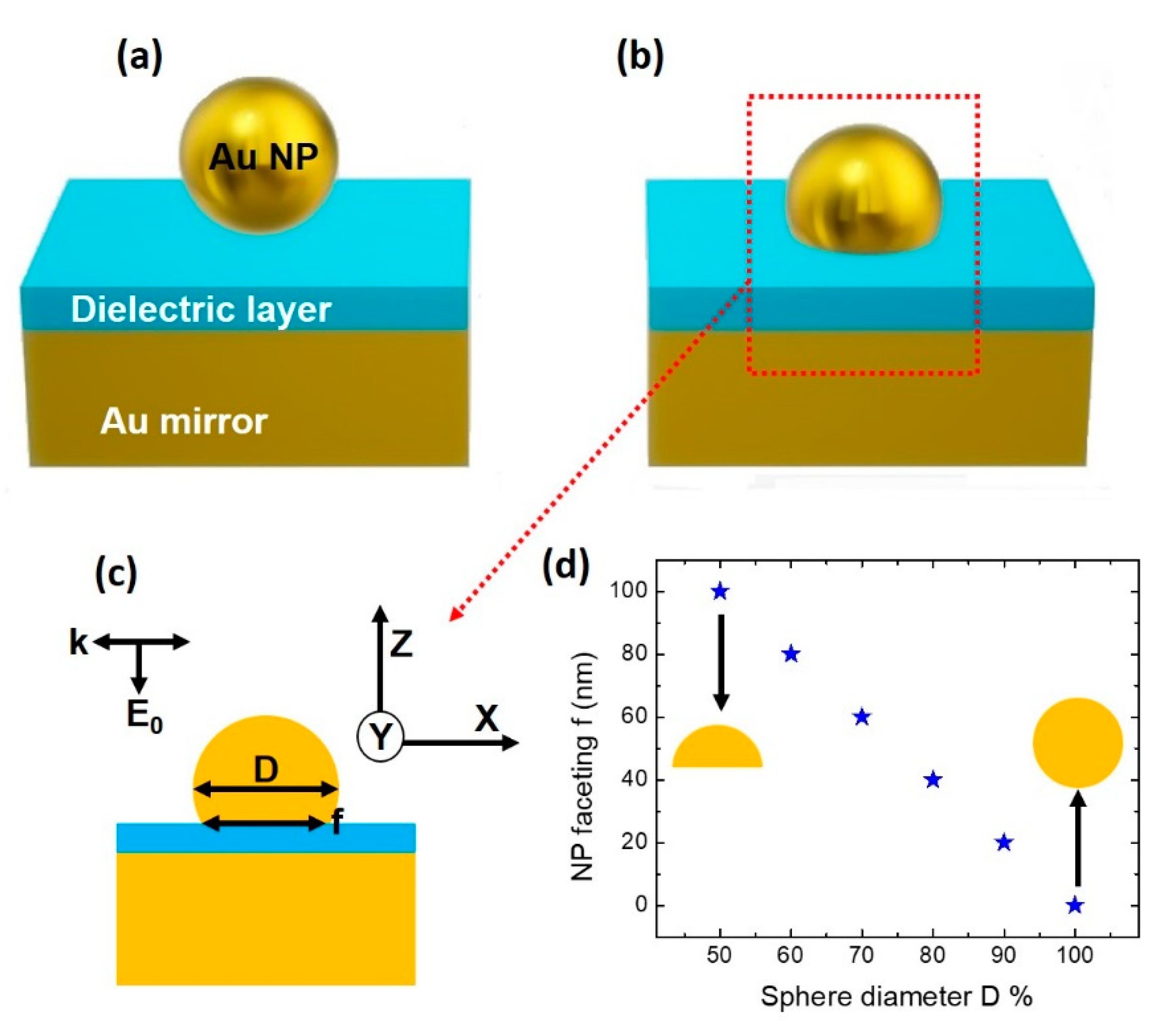
2. Materials and Methods

The schematic of the NPOM design is shown in Figure 1. An NP diameter “D” of 100 nm and a dielectric layer thickness of 2 nm were fixed throughout our simulations. The NP diameter was given by “D” and the faceting parameter “f” (in a circular shape) was introduced at the NP–dielectric interface (Figure 1a,b). The “f” parameter was related to the sphere “D” percentage (Figure 1c,d). A 100% sphere shape was formed when f = 0 nm. When “f” increased, NP faceting was introduced at the NP–dielectric interface. The hemisphere was structurally formed when “f” = 100 nm. Three-dimensional (3D) finite-difference time-domain (FDTD) was employed to analyze the optical characteristics of the NPOM plasmonic nanostructure (Lumerical Solutions Inc., Vancouver, Canada). The NPOM structure was excited with incident plane wave light E0 in “Z” direction in relation to the structure. The NPOM plasmonic nanostructure was surrounded by perfectly matched layers (PML). The high-resolution mesh size of 0.5 nm was employed to extract the proper solutions. A box field monitor was used to extract the broadband near field enhancement |E/E0|4 spectra. For this purpose, average near field enhancement spectroscopy was used to obtain the average integral volume of |E/E0|4 [6,12,14,17,36,37]:
Local   or   near   field   enhancement = | E / E 0 | 4 d v V  
Here, E (Ex, Ey, Ez) is the local electric field, E0 is the amplitude of the incident electric field and V is the volume at a certain distance limit (2 nm) within the metal–NP surface. In our NPOM simulation model, we used gold as a material for the NPs and metallic mirror. The refractive index of n = 1.5 was used for the dielectric layer. In the case of gold, the Johnson and Christy database was used and modeled by a Lorentz-Drude dispersion model fitting [42,43].
ϵ ( w ) = 1 f 0 w p 2 w ( w i Γ 0   ) + Σ j = 1 m   f j w p 2 ( w j 2   w 2 ) + i w Γ j
The parameters used in Equation (2) are explained as follows: Drude model fitting is shown as the first term in the equation where “wp” is the plasma frequency with “f0” oscillator strength and damping constant “Γ0”. The last term shows the Lorentz modification, where “m” represents a number of oscillations with frequency “wj”, damping constant “Γj” and strength “fj”.

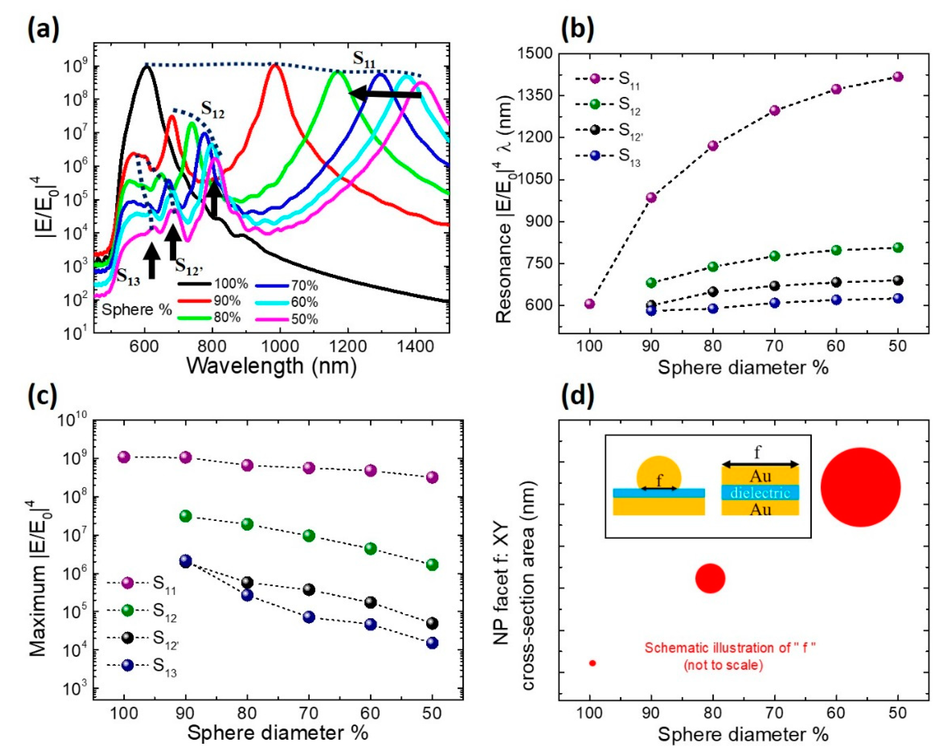
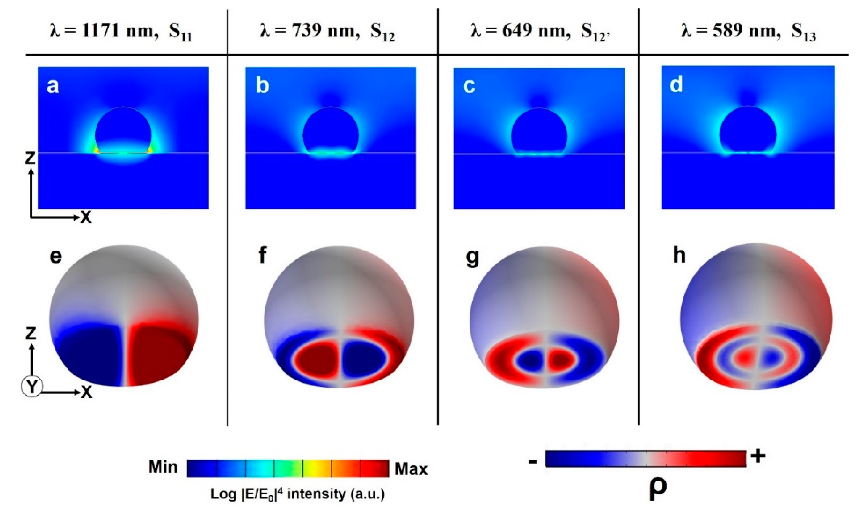
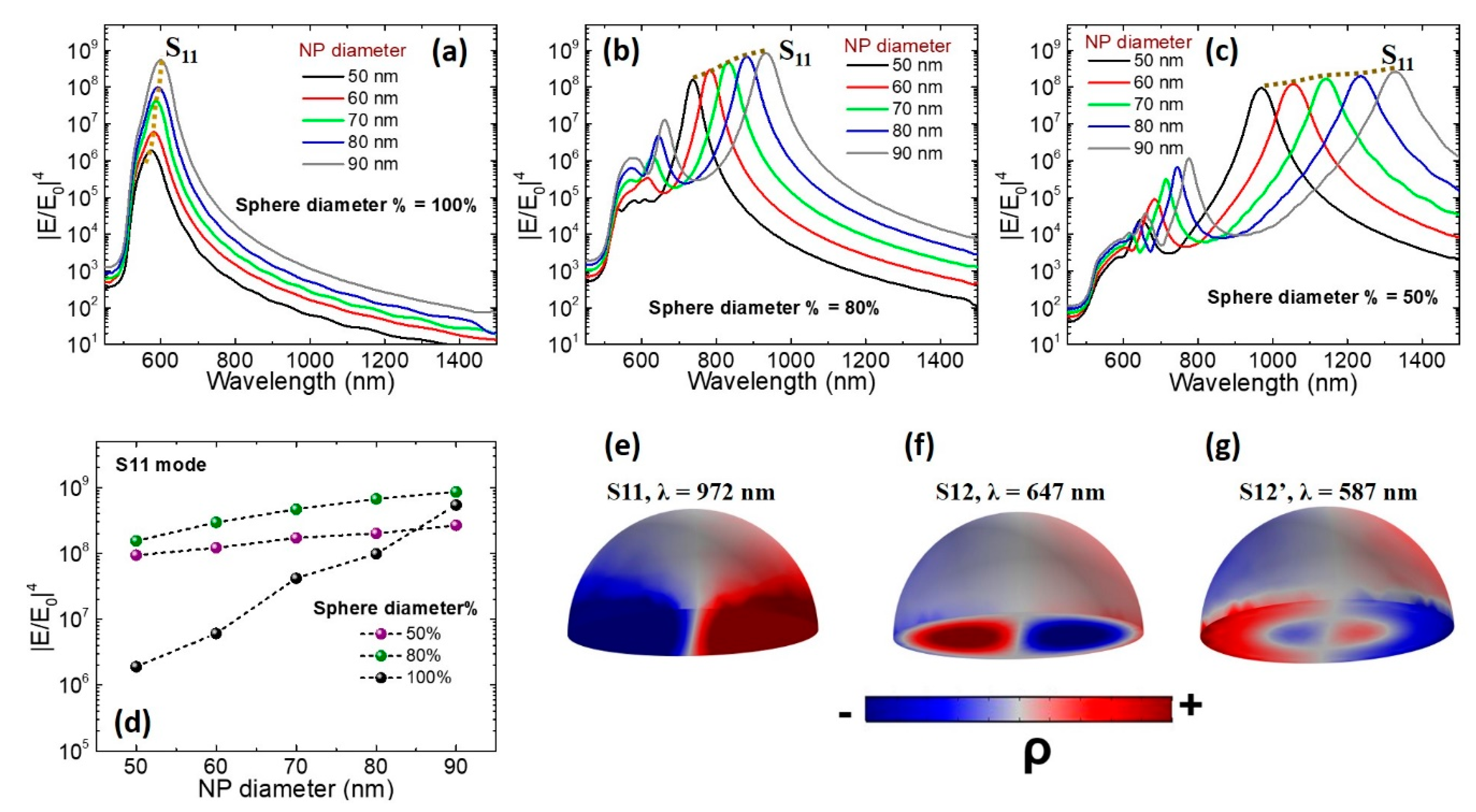
3. Results and Discussion

Three-dimensional FDTD simulation analysis of the 100% perfect sphere was carried out and structural modifications of NP faceting “f” were introduced by changing the sphere’s diameter “D” percentage (Figure 2). For the 100% sphere diameter, or perfect sphere, the resonance peak was found at 606 nm with a maximum near field intensity of |E/E0|4 of ~1 × 10⁹. As the sphere diameter D percentage decreased from 100%, a stronger red-shift was observed, and additional weaker resonance at shorter wavelengths arose. The dashed lines in Figure 2a indicate the resonance modes and are termed Smn (m = 1, n = 1, 2, 2′, 3). Their naming is further explained later in the Results section. One of the key results was the dominant S11 mode red-shifting its resonance to near-infrared at ~1.42 µm (NP at hemisphere shape) wavelength from a visible region (NP at perfect sphere shape) as sphere D% decreased (or as NP facet width “f” increased). Please note that despite the S11 mode resonance red-shift, the |E/E0|4 intensity decreased more slowly (from ~1 × 10⁹ to ~3.2 × 10⁸), which is helpful for SERS-based applications and device processing. This optical property showed that sphere diameter D% modification helped tune the S11 mode to the desired wavelength within a broad range (a span of ~800 nm till 50% sphere D% modification) with little compromise in terms of near field enhancement (Figure 2b,c).
At this point, we tried to understand the optical phenomenon behind the larger red-shift for the dominant S11 mode upon modification of the sphere diameter “D” percentage (or NP facet “f”). As shown in Figure 2d’s inset, the NPs on the film structure were approximated to a metal–insulator–metal (MIM) resonator [44,45,46]. For this kind of structure gap plasmons (cavity mode) exist, which is a type of electromagnetic wave strongly localized to the gap between metallic films that propagates along the plane of the film (for example, propagation along the x-axis and confinement along the y-axis) [46,47,48,49,50,51,52,53]. Upon light excitation, counter propagating gap plasmons formed standing waves, which was like the Fabry–Perot condition. Using the Fabry–Perot as the interpretation of resonances and an effective refractive index of the MIM cavity (neff), the resonance wavelength λmn of our current structure as a function of resonator width “f” was satisfied by the following equation [41,42,44,45,46]:
λ m n = ( f · π · n e f f ) / ( a m n   β )
Here β is an appropriate reflection phase, amn is the nth root of the mth order Bessel function Jm. In terms of mode labeling in the case of Smn, m denotes the number of angular modes and n represents the number of radial modes. From Equation (3), it is clearly visible that λmn is linearly proportional to resonator width f, which is an NP facet in our NPOM plasmonic structure. As schematically illustrated in Figure 2d, the circular NP facet area, as a function of percent of sphere diameter “D”, increased until it became a hemisphere. This explained the red-shift of the dominant S11 mode as well as other weaker resonance modes (S12, S12′ and S13) at shorter wavelengths.
To understand the mode properties, the electric field amplitude profiles of NPOM (sphere diameter D% = 80%) are shown in the XZ cross-section of Figure 3a–d. The XZ cross-sectional electric field profiles were extracted from S11 (λ = 1171 nm), S12 (λ = 739 nm), S12′ (λ = 649 nm) and S13 (λ = 589 nm) modes, as shown in Figure 2b. The maximum |E/E0|4 values obtained were in order of ~6.5 × 10⁸, 1.9 × 10⁷, 5.7 × 10⁵, 2.7 × 10⁵ for S11 to S13 modes respectively. Please note that in all S modes, the near field enhancement was dominantly observed from the cavity located at the NP–mirror region. As observed in the cross-sectional XZ electric field amplitude profiles, the number of nodes increased with the order of mode number. In order to deeply understand the complicated and hybridized plasmonic modes, it is good to utilize three-dimensional mapping of the surface charge distributions. This surface charge density (ρ) was calculated by considering the skin effect and by integrating Gauss’s law [38,41,42]:
ρ   =   ε 0 ( n x · E x +   n y · E y + n z · E z ) δ ( 1 e R / δ ) ρ   is   approximated   as   =   ( n x · E x +   n y · E y + n z · E z )
Here, the outward normal vector of the spherical NP surface is given by n = (nx, ny, nz), E = (Ex, Ey, Ez) is the local electric field, the permittivity of the vacuum is termed ε0, and δ is the skin depth [54,55]. Figure 3e–h shows the 3D mapping of surface charge distributions for NPs with facet modification for S11, S12, S12′ and S13 modes respectively. The 3D surface charge distributions clearly show the transverse dipole mode for the entire NP resonance in Figure 3e–h. Clear differences are seen in the NPOM hot spot or cavity area, where different orders of Fabry–Perot-like resonances were characterized. Please note that the difference between the S12 and S12′ modes was a charge switching of a similar number of nodes in the cavity of the NPOM structure. Here, the nodes were either confined inside the cavity area (S12′) or populated around the edges of the facet (S12), which is seen in Figure 3e–h. From the obtained electric amplitude profiles and 3D surface charge mapping, it is clearly understood that the cavity mode of NPOM plasmonic structures provides maximum contribution to the near field enhancement. The significant observation shows that the cavity modes are directly dependent on the NP faceting parameter.
In addition, gold NPs with diameters ranging from 50 to 90 nm were simulated to reveal the size-related effects. Faceting morphology changes based on a sphere diameter of 100%, 80% and 50% were studied for above mentioned NP sizes. Figure 4a–c shows the broadband near field spectrum for NP diameters of 50 to 90 nm as a function of sphere percentage, 100%, 80%, and 50%, respectively. In the case of a perfect sphere (Figure 4a), we saw the near field enhancement for S11 mode increase as NP diameter got bigger (~1.9 × 10⁶ for D = 50 nm, ~5.4 × 10⁸ for D = 90 nm). When the NP faceting effect was introduced, larger near field enhancements were observed for the dominant S11 mode wavelength while its resonance wavelength red-shifted, and additional weaker resonance modes (S12, S12′, S13) at shorter wavelengths were noted (Figure 4b,c). The most attractive feature to be pointed out was the role of the NP faceting effect in Figure 4d: for NPs with D = 50 nm, near field enhancement values of ~9.4 × 10⁷ and ~1.5 × 10⁸ were seen for 80% and 50% sphere diameters; more importantly their near field enhancements were very close to that of a bigger non-faceted NPs (D = 90 nm, ~5.4 × 10⁸). Thus, upon introducing a faceting morphology to smaller NPs (example D = 50 nm), it would be possible to extract larger near field enhancement close to that of larger NPs. Please note that similar optical properties can be observed with other commonly used plasmonic NP materials such as Ag, Al, etc. The only difference was the resonance position. The dielectric layer thickness parameter played a critical role in near field enhancement properties [36], but, most importantly, higher near field enhancement would be possible with 50% faceted NP D when compared with non-faceted NPs at similar dielectric spacer thickness conditions.
Figure 5 shows the data for S11, S12 and S13 radial mode resonance wavelength positions as a function of sphere diameter percentage (100%, 80%, 50%) for different NP Ds (50 to 90 nm). The dominant S11 radial mode was observed for all NP Ds and facet parameters. For non-faceted NPs, except in the presence of S11 radial mode, no other modes were present. As the faceting effect (e.g., 80% or 50%) was introduced to NP, additional radial modes (S12, S13) were seen. On the other hand, observation of additional radial modes was reduced even in the presence of faceting, based on the NP D. Figure 5c shows one such NP size related effect for smaller NP sizes (e.g., D = 50 and 60 nm, 50% sphere diameter) where S13 radial mode was absent. With our obtained data, it was possible to conclude that the number of radial modes was dependent on NP diameter size along with faceting “f” length. We hope that the possibility for high near field enhancement for smaller sized NPs upon faceting will boost several applications in the fields of plasmonics, photonics, and SERS-based sensors. Understanding the origin of radial mode numbers as a function of NP size and faceting effect will be helpful for optimizing practical near field enhancement-based applications.
Please note that previously reported tunable plasmonic nanostructures, for example, the most commonly used dimer designs involving bow-tie antenna, disks, spheres, or rods, showed limitations with large near field enhancement of surface modifications. Moreover, it is difficult to consistently fabricate or reproduce a gap as small as ~2 nm in plasmonic dimer nanoparticles. Whereas, in case of the NPOM design, with the help of recent advances in deposition techniques such as e-beam deposition, atomic layer deposition, and highly ordered self-assembly bio-fabrication methods, it is possible to deposit and reproduce a thinner dielectric layer [56,57,58]. Thus, practical fabrication of extremely small sized gaps of the NPOM plasmonic nanostructure is possible, and the process methodology is less complex when compared with other geometrical designs. Combined with the introduction of geometrical errors, such as NP faceting, retaining identical or little reduced near field enhancement characteristics will enhance flexibility of fabrication as well as optical characterization. By using a biopolymer layer (for example, genetically engineered M13 bacteriophage) as a dielectric spacer it is possible to realize a highly efficient plasmonic sensing device with high selectivity and sensitivity, which is critical for biosensor applications [58,59,60]. With the positives mentioned above, the NPOM plasmonic nanostructure introduces new possibilities for the high-precision analysis of optical properties and optoelectronic/photochemical processes, and interpretation of morphological changes at the sub-nanometer scale.

4. Conclusions

We simulated and numerically characterized effects of NP faceting, which structurally introduced modifications in the cavity of the NPOM plasmonic nanostructure. The variations in NP faceting introduced the following significant results: (i) the dominant S11 mode resonance wavelength was tuned in a span of ~800 nm from the visible to the near-infrared region where the sphere diameter “D” percentage was reduced from 100% to 50%; (ii) minimal reduction of S11 mode’s near field enhancement was noted even when NP facet structural modifications were introduced; (iii) the reason for S11 mode resonance tuning was found to be dependent on the NP facet “f” parameter; (iv) three-dimensional surface charge distributions revealed unchanged transverse dipolar mode characteristics of NPs and, at same time, revealed changes in the number of modes with respect to the S11, S12, S12′ and S13 order at the NPOM cavity; (v) NP faceting played a significant role practical device fabrication as the near field enhancement was negligibly affected even in the presence of sphere diameter variations from 100% to 50%. This means that, in-spite of the NP faceting error, a highly efficient plasmonic SERS device can still be realized. More importantly, it would be possible to demonstrate higher near field enhancement, in the order of ~109, from smaller sized NPs if a faceting morphological change were introduced (D = 50 nm, 50% sphere D). We hope that a better understanding of this sub-nanometer optical phenomenon in plasmonic nanostructures will be helpful for device fabrication and open up new opportunities in the fields of tunable (and high) near field enhancement SERS applications, biosensors, and so on.

Author Contributions

Conceptualization, V.D., C.K. and J.-W.O.; methodology, V.D., C.K.; validation, H.J., C.K. and V.D.; formal analysis, H.J. and J.-M.L.; investigation, V.D., H.J. and J.-W.O.; data curation, J.-M.L. and H.J.; writing—original draft preparation, V.D.; writing—review and editing, V.D.; H.J., J.-W.O.; visualization, J.-M.L.; supervision, J.-W.O.; project administration, J.-W.O.; funding acquisition, J.-W.O.

Funding

This work was supported by the National Research Foundation of Korea (NRF) Grant funded by the Korean Government (MSIP, MOE) (NRF-2016R1C1B2014423), the Creative Materials Discovery program of the National Research Foundation of Korea (NRF), funded by Ministry of Science and ICT (NRF-2017M3D1A1039287) and the Korea Institute of Planning and Evaluation for Technology in Food, Agriculture, Forestry (IPET) through the Advanced Production Technology Development Program of the Ministry of Agriculture, Food and Rural Affairs (MAFRA) (316080-04).

Conflicts of Interest

The authors declare no conflicts of interests.

References

  1. Schuller, J.A.; Barnard, E.S.; Cai, W.; Jun, Y.C.; White, J.S.; Brongersma, M.L. Plasmonics for extreme light concentration and manipulation. Nat. Mater. 2010, 9, 193–204. [Google Scholar] [CrossRef] [PubMed]
  2. Gramotnev, D.K.; Bozhevolnyi, S.I. Nanofocusing of electromagnetic radiation. Nat. Photonics 2014, 8, 13–22. [Google Scholar] [CrossRef]
  3. Gramotnev, D.K.; Bozhevolnyi, S.I. Plasmonics beyond the diffraction limit. Nat. Photonics 2010, 4, 83–91. [Google Scholar] [CrossRef]
  4. Barnes, W.L.; Dereux, A.; Ebbesen, T.W. Surface plasmon subwavelength optics. Nature 2003, 424, 824–830. [Google Scholar] [CrossRef]
  5. Han, Z.; Bozhevolnyi, S.I. Radiation guiding with surface plasmon polaritons. Rep. Prog. Phys. 2013, 76, 016402. [Google Scholar] [CrossRef]
  6. Jiang, N.; Zhuo, X.; Wang, J. Active plasmonics: Principles, structures, and applications. Chem. Rev. 2017, 118, 3054–3099. [Google Scholar] [CrossRef]
  7. Lal, S.; Link, S.; Halas, N.J. Nano-optics from sensing to waveguiding. Nat. Photonics 2007, 1, 641–648. [Google Scholar] [CrossRef]
  8. Lim, D.-K.; Jeon, K.-S.; Kim, H.M.; Nam, J.-M.; Suh, Y.D. Nanogap-engineerable Raman-active nanodumbbells for single-molecule detection. Nat. Mater. 2010, 9, 60–67. [Google Scholar] [CrossRef]
  9. Prodan, E.; Radloff, C.; Halas, N.J.; Nordlander, P. A hybridization model for the plasmon response of complex nanostructures. Science 2003, 302, 419–422. [Google Scholar] [CrossRef]
  10. Norlander, P.; Oubre, C.; Prodan, E.; Li, K.; Stockman, M.I. Plasmon hybridization in nanoparticle dimers. Nano Lett. 2004, 4, 899–903. [Google Scholar] [CrossRef]
  11. Xu, H.; Aizpurua, J.; Käll, M.; Apell, P. Electromagnetic contributions to single-molecule sensitivity in surface-enhanced Raman scattering. Phys. Rev. E 2000, 62, 4318–4324. [Google Scholar] [CrossRef] [Green Version]
  12. Devaraj, V.; Choi, J.; Kim, C.-S.; Oh, J.-W.; Hwang, Y.-H. Numerical analysis of nanogap effects in metallic nano-disk and nano-sphere dimers: High near-field enhancement with large gap sizes. J. Korean Phys. Soc. 2018, 72, 599–603. [Google Scholar] [CrossRef]
  13. Huang, Y.; Zhou, Q.; Hou, M.; Ma, L.; Zhang, Z. Nanogap effects on near- and far-field plasmonic behaviors of metallic nanoparticle dimers. Phys. Chem. Chem. Phys. 2015, 17, 29293–29298. [Google Scholar] [CrossRef] [PubMed]
  14. Li, J.F.; Huang, Y.F.; Ding, Y.; Yang, Z.L.; Li, S.B.; Zhou, X.S.; Fan, F.R.; Zhang, W.; Zhou, Z.Y.; Wu, D.Y.; et al. Shell-isolated nanoparticle-enhanced Raman spectroscopy. Nature 2010, 464, 392–395. [Google Scholar] [CrossRef] [PubMed]
  15. Schumacher, T.; Kratzer, K.; Molnar, D.; Hentschel, M.; Giessen, H.; Lippitz, M. Nanoantenna-enhanced ultrafast nonlinear spectroscopy of a single gold nanoparticle. Nat. Commun. 2011, 2, 333. [Google Scholar] [CrossRef] [Green Version]
  16. Luk’yanchuk, B.; Zheludev, N.I.; Maier, S.A.; Halas, N.J.; Nordlander, P.; Giessen, H.; Chong, C.T. The Fano resonance in plasmonic nanostructures and metamaterials. Nat. Mater. 2010, 9, 707–715. [Google Scholar] [CrossRef] [PubMed]
  17. Sperling, R.A.; Gil, P.R.; Zhang, F.; Zanella, M.; Parak, W.J. Biological applications of gold nanoparticles. Chem. Soc. Rev. 2008, 37, 1896–1908. [Google Scholar] [CrossRef] [PubMed]
  18. Wu, J.-L.; Chen, F.-C.; Hsiao, Y.-S.; Chien, F.-C.; Chen, P.; Kuo, C.-H.; Huang, M.H.; Hsu, C.-S. Surface plasmonic effects of metallic nanoparticles on the performance of polymer bulk heterojunction solar cells. ACS Nano 2011, 5, 959–967. [Google Scholar] [CrossRef] [PubMed]
  19. Wang, F.; Li, C.; Chen, H.; Jiang, R.; Sun, L.-D.; Li, Q.; Wang, J.; Yu, J.C.; Yan, C.-H. Plasmonic harvesting of light energy for suzuki coupling reactions. J. Am. Chem. Soc. 2013, 135, 5588–5601. [Google Scholar] [CrossRef] [PubMed]
  20. Li, L.; Hutter, T.; Steiner, U.; Mahajan, S. Single molecule SERS and detection of biomolecules with a single gold nanoparticle on a mirror junction. Analyst 2013, 138, 4574–4578. [Google Scholar] [CrossRef] [PubMed]
  21. Wei, L.; Lu, J.; Xu, H.; Patel, A.; Chen, Z.-S.; Chen, G. Silver nanoparticles: synthesis, properties, and therapeutic applications. Drug Discov. Today 2015, 20, 595–601. [Google Scholar] [CrossRef] [PubMed]
  22. Tang, F.; Boutami, S.; Adam, P.-M. Effect of metallic nanoparticles on improving the detection capacity of a micro-SERS sensor created by the hybrid waveguide of metallic slots and dielectric strips. ACS Omega 2018, 3, 4017–4026. [Google Scholar] [CrossRef]
  23. Hohenester, U.; Draxl, C. Ab initio approach for gap plasmonics. Phys. Rev. B 2016, 94, 165418. [Google Scholar] [CrossRef]
  24. Kravets, V.G.; Kabashin, A.V.; Barnes, W.L.; Grigorenko, A.N. Plasmonic surface lattice resonances: A review of properties and applications. Chem. Rev. 2018, 118, 5912–5951. [Google Scholar] [CrossRef] [PubMed]
  25. Fernández-Domínguez, A.I.; Maier, S.A.; Pendry, J.B. Collection and concentration of light by touching spheres: A transformation optics approach. Phys. Rev. Lett. 2010, 105, 266807. [Google Scholar] [CrossRef] [PubMed]
  26. Panaretos, A.H.; Yuwen, Y.A.; Werner, D.H.; Mayer, T.S. Tuning the optical response of a dimer nanoantenna using plasmonic nanoring loads. Sci. Rep. 2015, 5, 9813. [Google Scholar] [CrossRef] [PubMed] [Green Version]
  27. Fang, Z.; Fan, L.; Lin, C.; Zhang, D.; Meixner, A.J.; Zhu, X. Plasmonic coupling of bow tie antennas with ag nanowire. Nano Lett. 2011, 11, 1676–1680. [Google Scholar] [CrossRef]
  28. Tsai, C.-Y.; Lin, J.-W.; Wu, C.-Y.; Lin, P.-T.; Lu, T.-W.; Lee, P.-T. Plasmonic coupling in gold nanoring dimers: observation of coupled bonding mode. Nano Lett. 2012, 12, 1648–1654. [Google Scholar] [CrossRef]
  29. Lassiter, J.B.; McGuire, F.; Mock, J.J.; Ciracì, C.; Hill, R.T.; Wiley, B.J.; Chilkoti, A.; Smith, D.R. Plasmonic waveguide modes of film-coupled metallic nanocubes. Nano Lett. 2013, 13, 5866–5872. [Google Scholar] [CrossRef]
  30. Li, G.-C.; Zhang, Y.-L.; Jiang, J.; Luo, Y.; Lei, D.Y. Metal-substrate-mediated plasmon hybridization in a nanoparticle dimer for photoluminescence line-width shrinking and intensity enhancement. ACS Nano 2017, 11, 3067–3080. [Google Scholar] [CrossRef]
  31. Li, G.-C.; Zhang, Y.-L.; Lei, D.Y. Hybrid plasmonic gap modes in metal film-coupled dimers and their physical origins revealed by polarization resolved dark field spectroscopy. Nanoscale 2016, 8, 7119–7126. [Google Scholar] [CrossRef] [PubMed] [Green Version]
  32. Large, N.; Aizpurua, J.; Lin, V.K.; Teo, S.L.; Marty, R.; Tripathy, S.; Mlayah, A. Plasmonic properties of gold ring-disk nano-resonators: fine shape details matter. Opt. Express 2011, 19, 5587–5595. [Google Scholar] [CrossRef] [PubMed]
  33. Zhang, J.; Chen, S.; Wang, J.; Mu, K.; Fan, C.; Liang, E.; Ding, P. An engineered CARS substrate with giant field enhancement in crisscross dimer nanostructure. Sci. Rep. 2018, 8, 740. [Google Scholar] [CrossRef] [PubMed]
  34. Ciracì, C.; Hill, R.T.; Mock, J.J.; Urzhumov, Y.; Fernández-Domínguez, A.I.; Maier, S.A.; Pendry, J.B.; Chilkoti, A.; Smith, D.R. Probing the ultimate limits of plasmonic enhancement. Science 2012, 337, 1072–1074. [Google Scholar] [CrossRef] [PubMed]
  35. Mertens, J.; Eiden, A.L.; Sigle, D.O.; Huang, F.; Lombardo, A.; Sun, Z.; Sundaram, R.S.; Colli, A.; Tserkezis, C.; Aizpurua, J.; et al. Controlling subnanometer gaps in plasmonic dimers using graphene. Nano Lett. 2013, 13, 5033–5038. [Google Scholar] [CrossRef] [PubMed]
  36. Devaraj, V.; Lee, J.-M.; Oh, J.-W. Distinguishable plasmonic nanoparticle and gap mode properties in a silver nanoparticle on a gold film system using three-dimensional FDTD simulations. Nanomaterials 2018, 8, 582. [Google Scholar] [CrossRef] [PubMed]
  37. Huang, Y.; Ma, L.; Hou, M.; Li, J.; Xie, Z.; Zhang, Z. Hybridized plasmon modes and near-field enhancement of metallic nanoparticle-dimer on a mirror. Sci. Rep. 2016, 6, 30011. [Google Scholar] [CrossRef] [PubMed] [Green Version]
  38. Sigle, D.O.; Mertens, J.; Herrmann, L.O.; Bowman, R.W.; Ithurria, S.; Dubertret, B.; Shi, Y.; Yang, H.Y.; Tserkezis, C.; Aizpurua, J.; et al. Monitoring morphological changes in 2d monolayer semiconductors using atom-thick plasmonic nanocavities. ACS Nano 2014, 9, 825–830. [Google Scholar] [CrossRef] [PubMed]
  39. Devaraj, V.; Baek, J.; Jang, Y.; Jeong, H.; Lee, D. Design for an efficient single photon source based on a single quantum dot embedded in a parabolic solid immersion lens. Opt. Express 2016, 24, 8045–8053. [Google Scholar] [CrossRef] [PubMed]
  40. Tserkezis, C.; Esteban, R.; Sigle, D.O.; Mertens, J.; Herrmann, L.O.; Baumberg, J.J.; Aizpurua, J. Hybridization of plasmonic antenna and cavity modes: Extreme optics of nanoparticle-on-mirror nanogaps. Phys. Rev. A 2015, 92, 053811. [Google Scholar] [CrossRef] [Green Version]
  41. Huang, Y.; Ma, L.; Li, J.; Zhang, Z. Nanoparticle-on-mirror cavity modes for huge and/or tunable plasmonic field enhancement. Nanotechnology 2017, 28, 105203. [Google Scholar] [CrossRef] [PubMed]
  42. Johnson, P.B.; Christy, R.W. Optical constants of the noble metals. Phys. Rev. B 1972, 6, 4370–4379. [Google Scholar] [CrossRef]
  43. Markovic, M.I.; Rakic, A.D. Determination of the reflection coefficients of laser light of wavelengths λ∊(0.22 μm, 200 μm) from the surface of aluminum using the Lorentz-Drude model. Appl. Opt. 1990, 29, 3479–3483. [Google Scholar] [CrossRef] [PubMed]
  44. Minkowski, F.; Wang, F.; Chakrabarty, A.; Wei, Q.-H. Resonant cavity modes of circular plasmonic patch nanoantennas. Appl. Phys. Lett. 2014, 104, 021111. [Google Scholar] [CrossRef]
  45. Filter, R.; Qi, J.; Rockstuhl, C.; Lederer, F. Circular optical nanoantennas: an analytical theory. Phys. Rev. B 2012, 85, 125429. [Google Scholar] [CrossRef]
  46. Søndergaard, T.; Jung, J.; Bozhevolnyi, S.I.; Della Valle, G. Theoretical analysis of gold nano-strip gap plasmon resonators. New J. Phys. 2008, 10, 105008. [Google Scholar] [CrossRef]
  47. Nielsen, M.G.; Gramotnev, D.K.; Pors, A.; Albrektsen, O.; Bozhevolnyi, S.I. Continuous layer gap plasmon resonators. Opt. Express 2011, 19, 19310–19322. [Google Scholar] [CrossRef] [PubMed]
  48. Moreau, A.; Ciracì, C.; Mock, J.J.; Hill, R.T.; Wang, Q.; Wiley, B.J.; Chilkoti, A.; Smith, D.R. Controlled-reflectance surfaces with film-coupled colloidal nanoantennas. Nature 2012, 492, 86–89. [Google Scholar] [CrossRef] [Green Version]
  49. Nielsen, M.G.; Pors, A.; Albrektsen, O.; Bozhevolnyi, S.I. Efficient absorption of visible radiation by gap plasmon resonators. Opt. Express 2012, 20, 13311–13319. [Google Scholar] [CrossRef] [Green Version]
  50. Nielsen, M.G.; Bozhevolnyi, S.I. Highly confined gap surface plasmon modes in metal-strip-gap-film configurations. J. Opt. Soc. Am. B 2015, 32, 462–467. [Google Scholar] [CrossRef]
  51. Lee, Y.; Kamal, A.S.; Abasaki, M.; Ho, Y.-L.; Takakura, Y.; Delaunay, J.-J. Gap plasmons multiple mirroring from spheres in pyramids for surface-enhanced raman scattering. ACS Photonics 2016, 3, 2405–2412. [Google Scholar] [CrossRef]
  52. Ding, F.; Yang, Y.; Deshpande, R.A.; Bozhevolnyi, S.I. A review of gap-surface plasmon metasurfaces: fundamentals and applications. Nanophotonics 2018, 7, 1129–1156. [Google Scholar] [CrossRef]
  53. Stockman, M.I. Nanoplasmonics: past, present, and glimpse into future. Opt. Express 2011, 19, 22029–22106. [Google Scholar] [CrossRef] [PubMed] [Green Version]
  54. David, C.; García de Abajo, F.J. Surface plasmon dependence on the electron density profile at metal surfaces. ACS Nano 2014, 8, 9558–9566. [Google Scholar] [CrossRef] [PubMed]
  55. Seo, M.A.; Park, H.R.; Koo, S.M.; Park, D.J.; Kang, J.H.; Suwal, O.K.; Choi, S.S.; Planken, P.C.M.; Park, G.S.; Park, N.K.; et al. Terahertz field enhancement by a metallic nano slit operating beyond the skin-depth limit. Nat. Photonics 2009, 3, 152–156. [Google Scholar] [CrossRef]
  56. Mubeen, S.; Zhang, S.; Kim, N.; Lee, S.; Kramer, S.; Xu, H.; Moskovits, M. Plasmonic properties of gold nanoparticles seperated from a gold mirror by an ultrathin oxide. Nano Lett. 2012, 12, 2088–2094. [Google Scholar] [CrossRef]
  57. Park, Y.M.; Daniel, J.; Heeney, M.; Salleo, A. Room-temperature fabrication of ultrathin oxide gate dielectrics for low-voltage operation of organic field-effect transistors. Adv. Mater. 2011, 23, 971–974. [Google Scholar] [CrossRef]
  58. Oh, J.-W.; Chung, W.-J.; Heo, K.; Jin, H.-E.; Lee, B.Y.; Wang, E.; Zueger, C.; Wong, W.; Meyer, J.; Kim, C.; et al. Biomimetic virus-based colourimetric sensors. Nat. Commun. 2014, 5, 3043. [Google Scholar] [CrossRef] [Green Version]
  59. Lee, J.H.; Warner, C.M.; Jin, H.-E.; Barnes, E.; Poda, A.R.; Perkins, E.J.; Lee, S.-W. Production of tunable nanomaterials using hierarchically assembled bacteriophages. Nat. Protoc. 2017, 12, 1999–2013. [Google Scholar] [CrossRef]
  60. Lee, J.-M.; Choi, E.J.; Park, J.; Devaraj, V.; Kim, C.T.; Han, J.; Kim, W.-G.; Kim, K.; Kang, Y.-C.; Kim, K.H.; et al. Improvement of high affinity and selectivity on biosensors using genetically engineered phage by binding isotherm screening. Viruses 2019, 11, 248. [Google Scholar] [CrossRef]
Figure 1. (a) Schematic illustration of NP on a metallic mirror (NPOM) structure. Gold was employed as metal, and the dielectric layer was inserted between NP and the metallic film. Faceting parameter influence on NP morphology is shown in (b), and an example cross-section view is shown in (c). NP diameter changes (%) from a perfect sphere to a hemisphere as a function of the facet “f” parameter is shown in (d).
Coatings 09 00387 g001
Figure 2. (a) Broadband |E/E0|4 results for sphere diameter D% modification from 100% to 50% for NP D = 100 nm in NPOM plasmonic nanostructure. Resonance wavelengths (b) and near field intensities (c) for S11, S12, S12′ and S13 modes extracted from Figure 2a. (d) Schematic illustration of NP facet contact shape with a dielectric layer concerning sphere diameter % explaining the reason for the resonance red-shift. The inset figure displays the similarity of the metal–insulator–metal structure.
Coatings 09 00387 g002
Figure 3. Electric field amplitude and 3D surface charge distribution profiles taken from NPOM plasmonic structure with sphere “D” 80% for S11 (λ = 1171 nm), S12 (λ = 739 nm), S12′ (λ = 649 nm) and S13 (λ = 589 nm) modes. Cross-sectional XZ (ad) electric field amplitude profiles and related 3D surface charge distributions from NP standalone view (eh).
Coatings 09 00387 g003
Figure 4. (ac) Broadband |E/E0|4 spectrum for different NP diameters ranging from 50 to 90 nm as function of 100%, 80%, or 50% sphere diameter percentage in NPOM plasmonic structure. (d) Extracted maximum near field enhancement for S11 mode for different sphere D% from figures (ac). 3D surface charge distributions for S11, S12, and S12′ modes taken from hemispherical NPs with D = 50 nm (eg).
Coatings 09 00387 g004
Figure 5. Extracted resonance wavelengths for S11 mode (a), S12 mode (b), and S13 mode (c) obtained from broadband |E/E0|4 spectrum of Figure 4a–c.
Coatings 09 00387 g005

