Abstract
The internal coatings of chambers exposed to plasma over a long period of time are subject to chemical and physical damage. Contamination particles that are produced by plasma damage to coatings are a major contribution to poor process reliability. In this study, we investigated the behavior of contamination particles produced from plasma damage to Y2O3 and YF3 protective coatings, which were applied by an aerosol deposition method. The coating materials were located at the powered electrode, the grounded electrode, and the grounded wall, which were exposed to a NF3 plasma. The mass loss at the powered electrode, which was exposed to the NF3 plasma etching under an applied bias, showed that the YF3 etching rate was higher than that of Y2O3. Conversely, the mass of coating increased at the grounded electrode and the grounded wall, which were exposed to NF3 plasma etching under zero bias. The mass of the Y2O3 coating increased more than that of the YF3 coating. X-ray photoelectron spectroscopy analysis showed that the Y2O3 coating corroded to YOxFy in the NF3 plasma, and YF3 existed as YFx. Light scattering sensor analysis showed that the YF3 coating produced fewer contamination particles than did the Y2O3 coating.
1. Introduction
Efforts to minimize the influence of contamination particles, which are a major cause of decreased production yields, have been continuing as the degree of integration of semiconductor circuits has improved. There are various causes of contamination particles, including mechanical, chemical, and environmental factors. In particular, plasma used in processes for manufacturing semiconductors reacts with parts inside the chamber (e.g., electrodes, showerheads, liners, focusing rings, wall shield rings) to generate contamination particles.
Corroded particles grow on the surface of parts of the inner chamber, which are exposed to plasma ion bombardment and radical reactions over a long period of time. The weakly bonded corrosion particles then fall from the surface as the particles grow in size. As the process repeats, the plasma etches the surface and contamination particles fall off, becoming a major cause of process failure [1]. Corrosion and the extent of etching of parts of the surface are determined by the ion density and ion flux of the exposed plasma. A powered electrode which is exposed to a plasma etching under an applied bias is easily corroded and etched owing to collisions with a large energy flux. The grounded electrode and a grounded wall, which are exposed to a plasma etching under zero bias, sustain limited corrosion and etching by collisions with the ions, which have a low energy flux [2,3]. Ceramic coating films are used to prevent plasma corrosion at these surfaces and minimize the plasma corrosion [4,5,6,7]. Among ceramic coating materials for preventing plasma corrosion, Y2O3 is widely used for inner parts of the chamber because of its low etching rate and low chemical reactivity. Recently, YOF and YF3 have also drawn attention as ceramic coating materials for parts owing to their ability to suppress chemical reactions with fluoridated gases such as CF4 and NF3 [8,9,10,11,12,13]. Nevertheless, there have been few reports about the behavior of contamination particles by plasma etching [14]. Atmospheric plasma spraying (APS) methods are commonly used to coat parts with ceramic coating materials such as Y2O3 and YF3. The APS method melts a ceramic powder, with particles sizes in the range of several tens of micrometers, in a high-temperature plasma (10,000 K or more), which attaches to the substrate. The APS method enables the coating of thick films in a short period of time, but provides a rough surface and layered structure, such that the adhesion with the surface is poor and the coating peels off easily. Furthermore, such coatings have a low density owing to numerous internal pores [15]. The aerosol deposition (AD) method has been studied as a coating technology to overcome the limitations of APS. The AD method involves spraying a sub-micrometer-sized powder with high-pressure air through a nozzle in a vacuum chamber (>10−3 Torr). The AD method coats a high-density film with excellent uniformity of thickness compared with that of the APS method [16,17,18,19]. The plasma etching properties of ceramic coatings coated by the APS method have been reported in previous studies [8]; however, there is a lack of studies on the properties of ceramic coatings prepared by AD methods, including plasma etching properties and the generation of contamination particles. The etching properties of CF4 gas, which is used in the etching process, have been widely studied. However, etching with CF4 gas is often accompanied by the formation of unwanted fluorocarbon polymer layers. Recently, completely dissociated NF3 has been used to minimize these unwanted reactions and to achieve high etch rates [20,21,22,23].
In this study, we discuss the etching properties and contamination particles generation of Y2O3 and YF3 coatings fabricated by the AD method utilizing the NF3 plasma process. We investigated locations including the powered electrode, grounded electrode, and grounded wall to observe the etching characteristics of the coating material and the dependence on the bias voltage.
2. Materials and Methods
Figure 1 shows a schematic diagram of the capacitively coupled plasma system. The dimensions of the reactor were an inner diameter of 30 cm and a height of 30 cm. The powered electrode and grounded electrode had a radius of 7.6 cm. The discharge gap length from the powered electrode to the grounded electrode was 10 cm. Specimens were placed in the powered electrode, grounded electrode, and grounded wall, as shown in Figure 1.
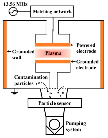
Figure 1.
Schematic diagram of the capacitively coupled plasma etching system. A specimen was placed in the powered electrode, grounded electrode, and grounded wall.
The NF3 gas was used to generate a plasma supplied through a showerhead with a mass flow controller. A dry pump and turbo pump were used in the vacuum system, and the working pressure of the experiment was 40 Pa. The power was set to be 13.56 MHz (Sizer Generator, Advanced Energy, Fort Collins, CO, USA), and an impedance matching network (Navigator, Advanced Energy, Fort Collins, CO, USA) was used to deliver the maximum power. The RF power applied to the plasma was 400 W. During the plasma etching, the temperatures at the powered electrode, grounded electrode, and grounded wall were about 120, 60, and 50 °C, respectively. The temperature was measured using an IR thermometer (IMPAC Pyrometer IN5, Lumasense Technologies, Santa Clara, CA, USA) and the temperature inside the chamber was measured through a viewport with zinc selenide.
The disc-like substrates were made of Al alloy 6061 and had a diameter of 76 mm and thickness of 1 mm. The substrates were then coated with Y2O3 and YF3 by AD, with the use of an aerosol deposition system (Dandan Corp., Daejeon, Korea), where Y2O3 and YF3 were in a powder form (99.99%, D50 = 0.5–5 µm). The sprayed coatings of Y2O3 and YF3 were 8 and 19 µm thick, respectively. The AD coating was performed as follows: the air flow rates were 40–80 SLM and the vacuum pressure was 10 Pa.
Before and after the NF3 plasma etching, the surface morphology and composition of the Y2O3 and YF3 coatings were ex-situ analyzed with a field-emission scanning electron microscope (FE-SEM, S-4800, Hitachi, Tokyo, Japan) and X-ray photoelectron spectroscopy (XPS; Monochromatic Al-Kα, AXIS-NOVA, Manchester, UK), respectively. The mass of the specimen was measured before and after the plasma etching test with a XP205 analytical balance (Mettler Toledo, Greifensee, Switzerland). After the plasma etching was performed for 60 min, the specimen was removed, and the mass loss was measured. The contamination particles produced from the Y2O3 and YF3 coatings were measured in real time according to the NF3 plasma exposure time. An ISPM light-scattering sensor (Stiletto, In Situ Particle Monitor, Inficon, Heidiland, Switzerland) was attached to the exhaust line to measure the amount and size of the contamination particles. This system was capable of measuring contamination particles in real time as they passed through the exhaust pipe. The ISPM was placed in the exhaust line so that it detected particles moving in one direction. The ISPM does not operate properly when exposed to the light of the plasma, because of excess noise. The minimum measurable particle size was ~0.2 µm. The sensor was based on the principles of laser light scattering, and more details of its working principles can be found in previous reports [24,25].
3. Results and Discussion
Figure 2 shows an FE-SEM image of Y2O3 and YF3 powders used as a starting material for coating. The Y2O3 powder (Figure 2a,b) and YF3 powder (Figure 2c,d) were composed of flat particles approximately 1–5 µm in size, and spherical particles approximately 0.5–1 µm in size, respectively. Furthermore, the YF3 powder showed greater aggregation than that of the Y2O3 powder. We expected that the YF3 powder was sprayed as a mixed powder, containing dispersed particles in the size range of 0.5–1 μm together with aggregated particles larger than 1 μm, because aggregated particles are not easily dispersed. When we applied the AD method, the Y2O3 and YF3 particles were sprayed by pressurized gas. The accelerated particles had a kinetic energy, which dissipated on collision with the substrate [17]. In this case, plastic deformation or fracturing of particles might occur owing to the high kinetic energy of large sprayed particles [18]. Particles tend to fracture when they aggregate or have a high kinetic energy owing to their large size, as shown in Figure 3.
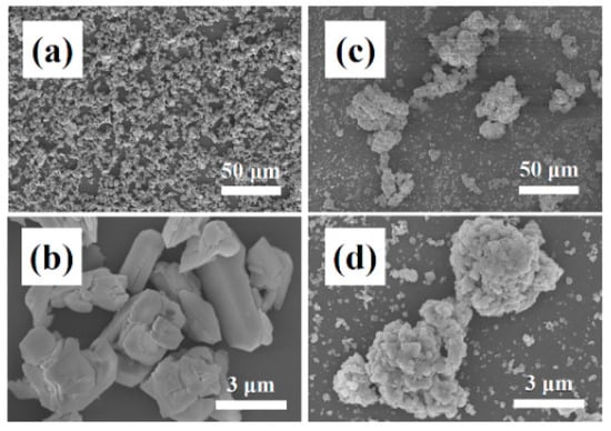
Figure 2.
FE-SEM images of Y2O3 and YF3 powders before coating by aerosol deposition: (a,b) Y2O3 powder and (c,d) YF3 powder.
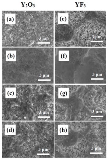
Figure 3.
FE-SEM images of the surface of Y2O3 and YF3 coatings before and after exposure to NF3 plasma: (a) Y2O3 and (e) YF3 before etching; (b) Y2O3 and (f) YF3 after etching of the powered electrode; (c) Y2O3 and (g) YF3 after etching of the grounded electrode; (d) Y2O3 and (h) YF3 after etching of the grounded wall.
The Y2O3 powder consisted of particles approximately 1–5 μm in size (Figure 2), and the Y2O3 particles were coated mainly by plastic deformation; however, fragmentation of larger particles into smaller particles was caused by their high kinetic energies at the moment of collision with the substrate. In this case, a film failed to form or only a residue formed (Figure 3a). The average particle size was 0.5–1 μm, but most aggregated YF3 particles were separated when they collided with the substrate, and formed a porous film. For this reason, before the NF3 plasma etching, the initial YF3 coating film (Figure 3e) and the Y2O3 coating film (Figure 3a) showed different surface properties. However, the final coating was denser than the initial coating film, because the initial coating was subjected to particles with high kinetic energy, which had a hammering effect. After the NF3 plasma etching, we confirmed that the coating surface changed depending on the position in the chamber. The Y2O3 (Figure 3b) and YF3 (Figure 3f) coatings on the powered electrode were rapidly corroded and etched. The NF3 plasma etching under an applied bias removed the initial surface and exposed a uniform surface, which was subjected to the hammering effect. Conversely, the Y2O3 (Figure 3c,d) and YF3 (Figure 3g,h) coatings at the grounded electrode and the grounded wall appeared to mix with the surface and took on a rough morphology similar to that of the powered electrode surface.
We attribute these surface properties to two factors. First, the surface was hardly corroded or etched by the NF3 plasma etching under zero bias. Rather, some by-products (contamination particles) were deposited, such as YOxFy or YFx, which were generated from etching of the powered electrode by NF3. As evidence for this change, we considered the mass change after exposure to the NF3 plasma (Figure 4). After exposure to NF3, the masses of the Y2O3 and YF3 coatings located on the powered electrode decreased (Figure 4a). The masses of the Y2O3 and YF3 coatings located on the grounded electrode and the grounded wall increased (Figure 4b,c).
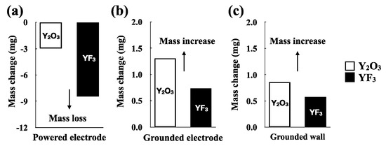
Figure 4.
Mass changes owing to the NF3 plasma etching: Y2O3 and YF3 coatings. (a) Y2O3 and YF3 after etching of the powered electrode; (b) Y2O3 and YF3 after etching of the grounded electrode; (c) Y2O3 and YF3 after etching of the grounded wall.
Next, the surfaces of the coating located on the grounded electrode and the grounded wall were maintained in the same state as before exposure to the NF3 plasma. The plasma density was highest at the center of the chamber and lower at the edges [26]. The grounded electrode and grounded wall were exposed to NF3 plasma etching under zero bias. Thus, the etching reaction occurred very slowly, and even after exposure to NF3 plasma, the Y2O3 coating on the grounded electrode and grounded wall contained very small particles generated by the fracturing of larger particles (Figure 3c,d), and the YF3 coating had a porous structure composed of fractured and aggregated particles (Figure 3g,h).
Finally, the coating of the grounded electrode showed a greater mass change than that of the grounded wall coating. If sputtering of by-products occurs, the grounded electrode will be more affected than the grounded wall because it is located directly below the powered electrode. Figure 4b,c shows that both the Y2O3 and YF3 coatings had a considerably greater mass increase for the grounded electrode compared with that for the grounded wall coating. In addition, the initial surface of the grounded wall (Figure 3d,h) showed better resistance than that of the grounded electrode (Figure 3c,g) for both the Y2O3 and YF3 coatings.
Compared with Y2O3, the YF3 coatings were more rapidly etched and showed greater mass loss under the NF3 plasma (Figure 4a). The standard boiling temperatures defined by IUPAC of Y2O3 and YF3 are 4570 and 2500 K, respectively, and the sublimation enthalpy of Y2O3 is also greater than that of YF3. Thus, Y2O3 forms stronger bonds than does YF3 [8]. Therefore, for an etching reaction occurring under the same conditions, YF3 is etched more rapidly than is Y2O3. We estimated the etching rates of the Y2O3 and YF3 coatings on the powered electrode from mass loss to be 48 and 186 nm/min/m2, respectively.
Notably, although the mass of the YF3 coating located on the powered electrode decreased considerably compared with that of the Y2O3 coating, the mass increases of the YF3 coatings located on the grounded electrode and the grounded electrode were less than those of the Y2O3 coating. This result is difficult to explain if simply considering the sputtering of by-products. We posit that fluorine deposition occurs in addition to the sputtering of by-products. Schaepkens et al. reported that fluorine gas takes precedence over etching where a self-bias voltage is present, and deposition occurred where the self-bias voltage was absent [27]. On this basis, we speculate that fluorine deposition occurred on the grounded electrode and grounded wall where the self-bias voltage was absent. In particular, the Y2O3 coating was more greatly affected by fluorine deposition than the YF3 coating because of the many oxygen atoms and vacancies that can react with fluorine. As a result, by-product sputtering and fluorine deposition occurred at the same time in the coating of the grounded wall and grounded electrode during exposure to NF3 plasma. The Y2O3 coating mass greatly increased because the Y2O3 coating was affected more by the fluorine deposition reaction than was the YF3 coating. On the other hand, the YF3 coating was affected more by the sputtering of by-product reaction than the fluorine deposition reaction.
We had previously confirmed that the Y2O3 coating reacts with NF3 plasma to form YOxFy, which is etched by ion attack, and the YOxFy coating is etched in the form of YOxFy without a principal chemical reaction [8]. On the basis of previous studies, the YF3 coating is also expected to be etched in the form of YFx without notable chemical corrosion reactions (Figure 5). We measured the amounts of Y, O, and F in the Y2O3 and YF3 coatings by XPS analysis after exposure to NF3 plasma to confirm the etching mechanism (Table 1). The YF3 coating showed no notable component changes before and after exposure to NF3 plasma. However, the Y2O3 coating had a lower O 1s content and a greater F 1s content.
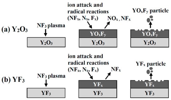
Figure 5.
Schematic diagram of yttrium oxyfluoride film deposition and etching behavior of (a) Y2O3 and (b) YF3 coatings.

Table 1.
X-ray photoelectron spectroscopy (XPS) analysis results of Y2O3 and YF3 coatings before and after exposure to NF3 plasma: (a) Y2O3 and (e) YF3 before etching; (b) Y2O3 and (f) YF3 after etching of the powered electrode; (c) Y2O3 and (g) YF3 after etching of the grounded electrode; (d) Y2O3 and (h) YF3 after etching of the grounded wall.
Figure 6 shows the XPS spectra of yttrium in Y2O3 and YF3 before and after the NF3 plasma treatment for more precise analysis. We designated the XPS peaks for the cations of Y 3d5/2 and Y 3d3/2 as blue, green, and orange lines, respectively. The binding energy difference of the two peaks was 2.05 eV, which represents an intensity ratio of 3:2. The Y 3d5/2 and Y 3d3/2 spectra were fitted by a ratio of 10:90 (Gaussian/Lorentzian). In the case of Y2O3 before the reaction with NF3 plasma, the Y 3d5/2 peak positions (green line) were 157.8 and 156.2 eV, and the Y 3d3/2 peak positions (orange line) were 160.1 and 158.3 eV. However, after the reaction with the NF3 plasma, the binding energy of Y 3d5/2 (blue line) and Y 3d3/2 shifted to 159 and 161.5 eV, respectively; hence, Y–F bonds formed.
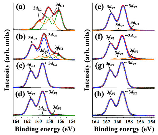
Figure 6.
X-ray photoelectron spectroscopy (XPS) results: (a) Y2O3 and (e) YF3 before etching, (b) Y2O3 and (f) YF3 after etching of the powered electrode; (c) Y2O3 and (g) YF3 after etching of the grounded electrode; (d) Y2O3 and (h) YF3 after etching of the grounded wall.
Figure 6a shows the three Y–O peaks located at 159.9, 158.1, and 156.2 eV (red line). As shown in Figure 6b–d, the peak position shifted to higher binding energy after the reaction with the NF3 plasma. Because the F ion has a very high electron affinity, the binding length with the cation X was shortened, the electron density was decreased, and the binding energy increased when the X–O bond was substituted with the X–F bond [7]. After the reaction with the NF3 plasma, the Y–O bonds were substituted with Y–F bonds, and the binding energy increased owing to the difference in electronegativity between the two bonds. This result confirms that the Y2O3 coating of the powered electrode featured coexisting Y–O and Y–F bonds because the surface of Y2O3 coating was etched. At the grounded electrode and the grounded wall, the Y–O bonds on the surface were completely substituted by Y–F owing to the high reactivity of fluorine radicals; hence, the surface had an apparent binding energy peak similar to that of YF3. Conversely, as shown in Figure 6e–h, the YF3 coating exhibited less change in its composition before and after NF3 plasma treatment. As a result, we confirmed that the previously expected mechanisms for the reaction of the NF3 plasma with Y2O3 and YF3 coatings were reasonable.
Finally, we measured the contamination particles generated in real time in the NF3 plasma environment for 60 min in order to confirm the formation behavior of contaminating particles from the Y2O3 and YF3 coatings (Figure 7). Figure 7 shows the concentration and the cumulative concentration of contamination particles generated in real time. During the initial 10 min, contaminating particles were rarely generated at the Y2O3 and YF3 coating films. This is thought to be due to the growth mechanism of the contamination particles and the surface temperature change of the powered electrode by plasma applied bias. The contamination particles initially grow on the coating surface, and the grown contamination particles are dropped off at the weakened bond sites. Also, the surface temperature of the powered electrode was increased to 120 °C while being heated by plasma applied bias, and then maintained at 120 °C by cooling systems. When the coating material reached 120 °C, the coating films became stressed because of the difference in the thermal expansion coefficient between the aluminum used as the base material and the coating material, and grown contamination particles more easily fell off from the surface. Hence, during the initial 10 min, contaminating particles were rarely generated because it takes time to grow contamination particles and raise the temperature of the powered electrode. The results show that more contamination particles were generated in the Y2O3 coating. This finding contradicts the results of mass loss measurements by etching of the YF3 and Y2O3 coatings, as discussed previously. As mentioned above, Y2O3 reacted with the NF3 plasma to produce YOxFy, a volatile gas, and NOx. The YF3 produced YFx and NFx gas without any notable chemical changes (Figure 5). Hence, the chemical corrosion of the Y2O3 coating was faster when subjected to NF3 plasma than was the YF3 coating, which means that the contamination particles grew faster on the Y2O3 coating surface than on the YF3 coating. However, Y2O3 has a higher binding energy than that of YF3; hence, the growth of contamination particles from the Y2O3 coating was slower than for the YF3 coating.
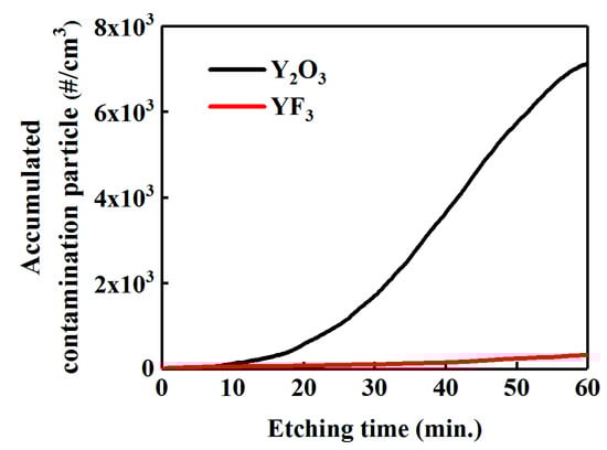
Figure 7.
Real-time detection of accumulated contamination particle concentration, over 0.2 μm size, generated from Y2O3 and YF3 during the 60 min NF3 plasma treatment.
As a result, YF3 is stable to chemical corrosion when subject to the NF3 plasma; however, the weak physical binding force resulted in rapid etching and produced fewer contamination particles of a critical size, which could act as defects in the actual plasma process. The Y2O3 was slowly etched because of the strong physical binding forces, but was susceptible to chemical corrosion by the NF3 plasma, which caused large contamination particles, which act as defects in the actual plasma process [18,22].
4. Conclusions
We prepared Y2O3 and YF3 coatings by AD and subjected these to NF3 plasma. Owing to the characteristics of the starting materials, the initial surfaces had different properties. However, the Y2O3 and YF3 coatings placed at the powered electrode were rapidly etched by the NF3 plasma treatment. Less etching occurred at the grounded electrode and the grounded walls, and the mass at these surfaces increased owing to sputtering of by-products and fluorine deposition. Additionally, the Y2O3 coating showed more rapid chemical corrosion than did the YF3 coating, and many contamination particles were generated, which acted as defects. This study demonstrates that the YF3 coating has the potential to be used as a candidate material to reduce contaminating particles in the semiconductor etching process.
Author Contributions
Conceptualization, J.-B.S. and E.C.; Methodology, J.-B.S.; Investigation, J.-B.S. and E.C.; Writing—Original Draft Preparation, J.-B.S. and E.C.; Writing—Review and Editing, J.-B.S., E.C., J.-T.K., S.-G.O., and J.-Y.Y.; Supervision, J.-T.K., S.-G.O., and J.-Y.Y.
Funding
This research was funded by the R&D Convergence Program of National Research Council of Science and Technology (NST) of the Republic of Korea (NST, CAP-16-04-KRISS) and Development of Fundamental Technology for Industrial Metrology funded by Korea Research Institute of Standards and Science (KRISS-2019-GP2019-0011).
Acknowledgments
We would like to Kang-Ho Lee and Jung-Nam Park of Dandan Corporation for providing aerosol-deposited Y2O3 and YF3 coatings. We are thankful to our colleagues Seung-Su Lee, Minjoong Kim, and Jong-Ho So, who assisted with some experiments.
Conflicts of Interest
The authors declare no conflict of interest.
References
- Kasashima, Y.; Nabeoka, N.; Motomura, T.; Uesugi, F. Many flaked particles caused by impulsive force of electric field stress and effect of electrostriction stress in mass-production plasma etching equipment. Jpn. J. Appl. Phys. 2014, 53, 040301. [Google Scholar] [CrossRef]
- Chu, P.K.; Qin, S.; Chan, C.; Cheung, N.W.; Ko, P.K. Instrumental and process considerations for the fabrication of silicon-on-insulators (SOI) structures by plasma immersion ion implantation. IEEE Trans. Plasma Sci. 1998, 26, 79–84. [Google Scholar] [CrossRef][Green Version]
- Yang, Y.; Kushner, M.J. Modeling of dual frequency capacitively coupled plasma sources utilizing a full-wave Maxwell solver: II. Scaling with pressure, power and electronegativity. Plasma Sources Sci. Technol. 2010, 19, 055012. [Google Scholar] [CrossRef]
- Shin, J.S.; Kim, M.; Song, J.B.; Jeong, N.G.; Kim, J.T.; Yun, J.Y. Fluorine plasma corrosion resistance of anodic oxide film depending on electrolyte temperature. Appl. Sci. Converg. Technol. 2018, 27, 9–13. [Google Scholar] [CrossRef]
- Song, J.B.; Kim, J.T.; Oh, S.G.; Shin, J.S.; Chun, J.R.; Yun, J.Y. Effect of sealing time of anodic aluminum oxide (AAO) film for preventing plasma damage. Sci. Adv. Mater. 2015, 7, 127–132. [Google Scholar] [CrossRef]
- Cao, Y.C.; Zhao, L.; Luo, J.; Wang, K.; Zhang, B.P.; Tokota, H.; Ito, Y.; Li, J.F. Plasma etching behavior of Y2O3 ceramics: Comparative study with Al2O3. Appl. Surf. Sci. 2016, 366, 304–309. [Google Scholar] [CrossRef]
- Kim, D.M.; Lee, S.H.; Alexander, W.B.; Kim, K.B.; Oh, Y.S.; Lee, S.M. X-ray photoelectron spectroscopy study on the interaction of yttrium-aluminum oxide with fluorine-based plasma. J. Am. Ceram. Soc. 2011, 94, 3455–3459. [Google Scholar] [CrossRef]
- Tahara, R.; Tsunoura, T.; Yoshida, K.; Yano, T.; Kishi, Y. Fabrication of dense yttrium oxyfluoride ceramics by hot pressing and their mechanical, thermal, and electrical properties. Jpn. J. Appl. Phys. 2018, 57, 06JF04. [Google Scholar] [CrossRef]
- Lin, T.K.; Wuu, D.S.; Huang, S.Y.; Wang, W.K. Preparation and characterization of sprayed-yttrium oxyfluoride corrosion protective coating for plasma process chambers. Coatings 2018, 8, 373. [Google Scholar] [CrossRef]
- Wang, W.K.; Lin, Y.X.; Xu, Y.J. Structural and fluorine plasma etching behavior of sputter-deposition yttrium fluoride film. Nanomaterials 2018, 8, 936. [Google Scholar] [CrossRef]
- Ma, T.; List, T.; Donnelly, V.M. Comparisons of NF3 plasma-cleaned Y2O3, YOF, and YF3 chamber coatings during silicon etching in Cl2 plasmas. J. Vac. Sci. Technol. A Vac. Surf. Films 2018, 36, 0734. [Google Scholar] [CrossRef]
- Shiba, Y.; Teramoto, A.; Goto, T.; Kishi, Y.; Shirai, Y.; Sugawa, S. Stable yttrium oxyfluoride used in plasma process chamber. J. Vac. Sci. Technol. A Vac. Surf. Films 2017, 35, 021405. [Google Scholar] [CrossRef]
- Kim, D.M.; Jang, M.R.; Oh, Y.S.; Kim, S.; Lee, S.M.; Lee, S.H. Relative sputtering rates of oxides and fluorides of aluminum and yttrium. Surf. Coat. Technol. 2017, 309, 694–697. [Google Scholar] [CrossRef]
- Song, J.B.; Kim, J.T.; Oh, S.G.; Yun, J.Y. Contamination particles and plasma etching behavior of atmospheric plasma sprayed Y2O3 and YF3 coatings under NF3 plasma. Coatings 2019, 9, 102. [Google Scholar] [CrossRef]
- Pawlowski, L. The Science and Engineering of Thermal Spray Coatings, 2nd ed.; John Wiley & Sons: Chichester, UK, 2008. [Google Scholar]
- Fan, W.; Bai, Y. Review of suspension and solution precursor plasma sprayed thermal barrier coatings. Ceram. Int. 2016, 42, 14299–14312. [Google Scholar] [CrossRef]
- Hanft, D.; Exner, J.; Schubert, M.; Stöcker, T.; Fuierer, P.; Moos, R. An overview of the aerosol deposition method: Process fundamentals and new trends in materials applications. J. Ceram. Sci. Technol. 2015, 6, 147–182. [Google Scholar] [CrossRef]
- Akedo, J. Aerosol deposition of ceramic thick films at room temperature: Densification mechanism of ceramic layers. J. Am. Ceram. Soc. 2006, 89, 1834–1839. [Google Scholar] [CrossRef]
- Choi, H.; Kim, K.; Choi, H.; Kang, S.; Yun, J.; Shin, Y.; Kim, T. Plasma resistant aluminum oxide coatings for semiconductor processing apparatus by atmospheric aerosol spray method. Surf. Coat. Technol. 2010, 205, S125–S128. [Google Scholar] [CrossRef]
- Machima, P.; Hershkowitz, N. SiO2 and Si3N4 etch mechanisms in NF3/hydrocarbon plasma. J. Phys. D Appl. Phys. 2006, 39, 673. [Google Scholar] [CrossRef]
- Ji, B.; Yang, J.H.; Badowski, P.R.; Karwacki, E.J. Optimization and analysis of NF3 in situ chamber cleaning plasmas. J. Appl. Phys. 2004, 95, 4452–4462. [Google Scholar] [CrossRef]
- Kastenmeir, B.E.E.; Matsuo, P.J.; Oehrlein, G.S.; Langan, J.G. Remote plasma etching of silicon nitride and silicon dioxide using NF3/O2 gas mixtures. J. Vac. Sci. Technol. A Vas. Surf. Films 1998, 16, 2047–2056. [Google Scholar] [CrossRef]
- Matsuo, P.J.; Kastenmeier, B.E.E.; Oehrlein, G.S.; Langan, J.G. Silicon etching in NF3/O2 remote microwave plasmas. J. Vac. Sci. Technol. A Vas. Surf. Films 1999, 17, 2431–2434. [Google Scholar] [CrossRef]
- Miyashita, H.; Kikuchi, T.; Kawasaki, Y.; Katakura, Y.; Ohsako, N. Particle measurements in vacuum tools by in situ particle monitor. J. Vac. Sci. Technol. A Vac. Surf. Films 1999, 17, 1066–1070. [Google Scholar] [CrossRef]
- Hulst, H.C. Light Scattering by Small Particles; Dover Publications, Inc.: New York, NY, USA, 1981. [Google Scholar]
- Lee, H.C.; Bang, J.Y.; Chung, C.W. Effects of RF bias power on electron energy distribution function and plasma uniformity in inductively coupled argon plasma. Thin Solid Films 2011, 519, 7009–7013. [Google Scholar] [CrossRef]
- Schaepkens, M.; Oehrlein, G.S. A review of SiO2 etching studies in inductively coupled fluorocarbon plasmas. J. Electrochem. Soc. 2001, 148, C211–C221. [Google Scholar] [CrossRef]
© 2019 by the authors. Licensee MDPI, Basel, Switzerland. This article is an open access article distributed under the terms and conditions of the Creative Commons Attribution (CC BY) license (http://creativecommons.org/licenses/by/4.0/).