The Seebeck Coefficient of Sputter Deposited Metallic Thin Films: The Role of Process Conditions


Abstract
1. Introduction
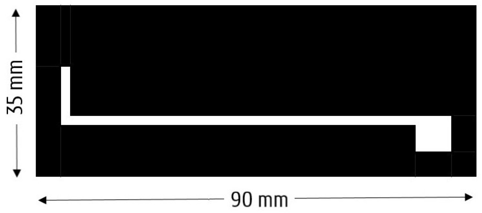
2. Materials and Methods
3. Results
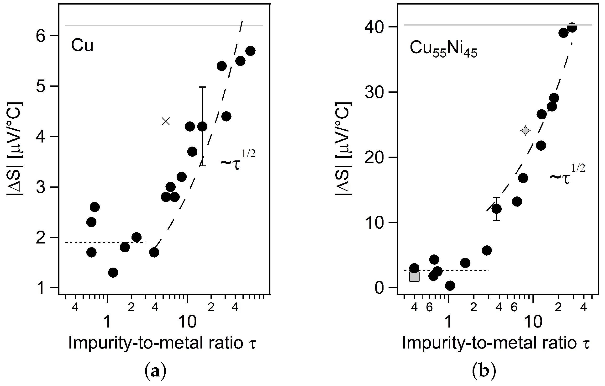
3.1. Impurities
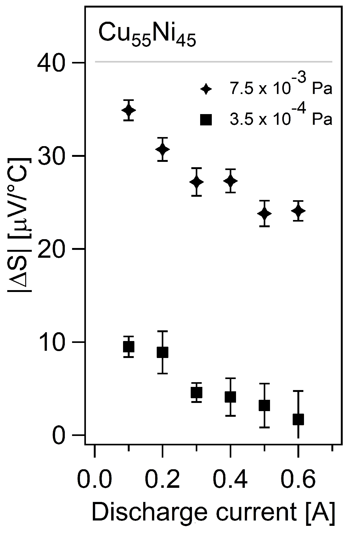
3.2. Discharge Current
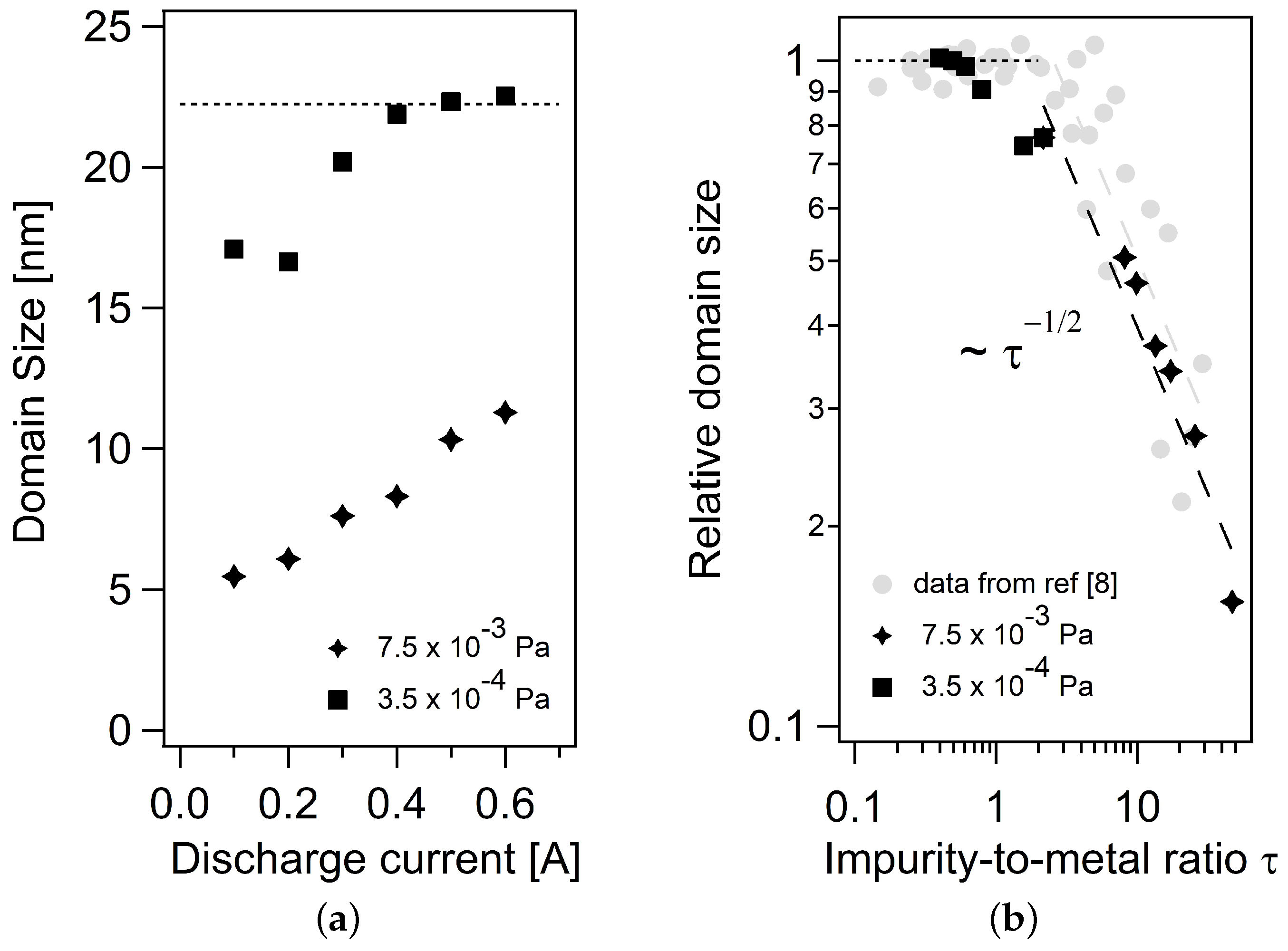
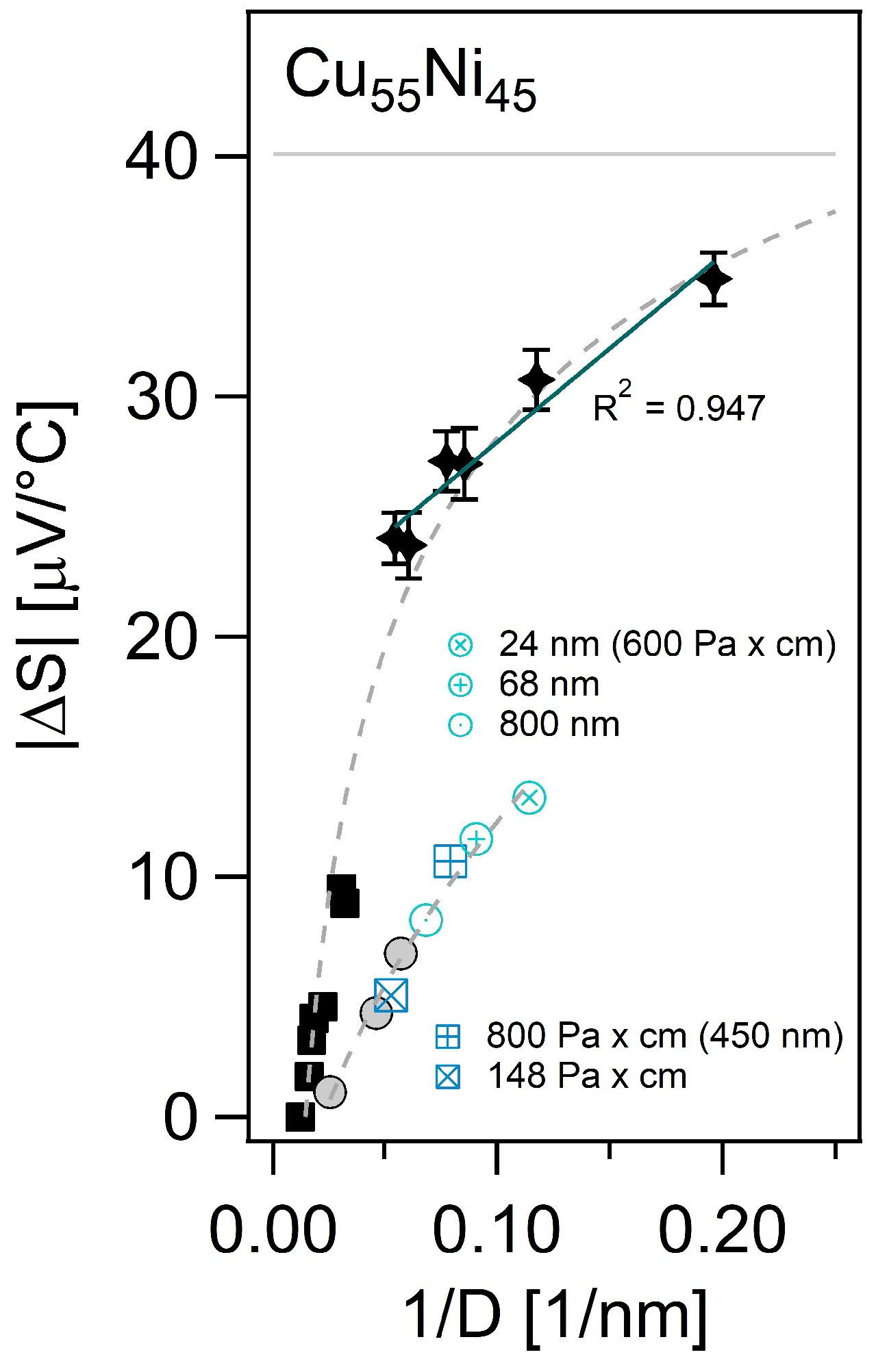
3.3. Domain Size
4. Discussion
4.1. Role of Layer Thickness
4.2. Process Parameters
4.3. Impurities
5. Conclusions
Author Contributions
Funding
Conflicts of Interest
Abbreviations
| EPA | Energy per arriving adatom |
| P | Argon Pressure |
| d | Target-to-substrate distance |
| D | Domain Size |
| t | Layer thickness |
| FWHM | Full width at half maximum |
| RF | Radio-frequent |
| DC | Direct-current |
| RCA | Radio Corporation of America |
| MS | Mayadas-Shatzkes |
| PID | Proportional-integral-derivative |
| XRD | X-ray diffraction |
| TEM | Transmission electron microscope |
| AFM | Atomic force microscopy |
| EBSD | Electron backscatter diffraction |
References
- Laugier, M. The construction and use of thin film thermocouples for the measurement of surface temperature: Applications to substrate temperature determination and thermal bending of a cantilevered plate during film deposition. Thin Solid Films 1980, 67, 163–170. [Google Scholar] [CrossRef]
- Kreider, K.G. Sputtered high temperature thin film thermocouples. J. Vac. Sci. Technol. A Vac. Surf. Films 1993, 11, 1401–1405. [Google Scholar] [CrossRef]
- Scarioni, L.; Castro, E. Thermoelectric power in thin film Fe–CuNi alloy (type-J) couples. J. Appl. Phys. 2000, 87, 4337–4339. [Google Scholar] [CrossRef]
- Chopra, K.; Bahl, S.; Randlett, M. Thermopower in thin-film copper—Constantan couples. J. Appl. Phys. 1968, 39, 1525–1528. [Google Scholar] [CrossRef]
- Guo, H.; Jiang, J.Y.; Liu, J.X.; Nie, Z.H.; Ye, F.; Ma, C.F. Fabrication and Calibration of Cu-Ni Thin Film Thermocouples. Adv. Mater. Res. 2012, 512–515, 2068–2071. [Google Scholar] [CrossRef]
- Sadat, S.; Tan, A.; Chua, Y.J.; Reddy, P. Nanoscale thermometry using point contact thermocouples. Nano Lett. 2010, 10, 2613–2617. [Google Scholar] [CrossRef] [PubMed]
- Kim, K.; Jeong, W.; Lee, W.; Reddy, P. Ultra-high vacuum scanning thermal microscopy for nanometer resolution quantitative thermometry. Acs Nano 2012, 6, 4248–4257. [Google Scholar] [CrossRef]
- Kim, K.; Song, B.; Fernández-Hurtado, V.; Lee, W.; Jeong, W.; Cui, L.; Thompson, D.; Feist, J.; Reid, M.H.; García-Vidal, F.J.; et al. Radiative heat transfer in the extreme near field. Nature 2015, 528, 387. [Google Scholar] [CrossRef]
- Liu, H.; Sun, W.; Xiang, A.; Shi, T.; Chen, Q.; Xu, S. Towards on-chip time-resolved thermal mapping with micro-/nanosensor arrays. Nanoscale Res. Lett. 2012, 7, 484. [Google Scholar] [CrossRef]
- Li, G.; Wang, Z.; Mao, X.; Zhang, Y.; Huo, X.; Liu, H.; Xu, S. Real-time two-dimensional mapping of relative local surface temperatures with a thin-film sensor array. Sensors 2016, 16, 977. [Google Scholar] [CrossRef]
- Guk, E.; Ranaweera, M.; Venkatesan, V.; Kim, J.S. Performance and durability of thin film thermocouple array on a porous electrode. Sensors 2016, 16, 1329. [Google Scholar] [CrossRef] [PubMed]
- Meredith, R.D.; Wrbanek, J.D.; Fralick, G.C.; Greer, L.C.; Hunter, G.W.; Chen, L. Design and operation of a fast, thin-film thermocouple probe on a turbine engine. In Proceedings of the 50th AIAA/ASME/SAE/ASEE Joint Propulsion Conference, Cleveland, OH, USA, 28–30 July 2014; p. 3923. [Google Scholar]
- Zeng, Q.Y.; Hong, T.; Chen, L.; Cui, Y.X. Magnetron sputtering of NiCr/NiSi thin-film thermocouple sensor for temperature measurement when machining chemical explosive material. Key Eng. Mater. 2011, 467, 134–139. [Google Scholar] [CrossRef]
- Geballe, T.; Hull, G. Seebeck effect in silicon. Phys. Rev. 1955, 98, 940. [Google Scholar] [CrossRef]
- Gayner, C.; Kar, K.K. Recent advances in thermoelectric materials. Prog. Mater. Sci. 2016, 83, 330–382. [Google Scholar] [CrossRef]
- Marshall, R.; Atlas, L.; Putner, T. The preparation and performance of thin film thermocouples. J. Sci. Instrum. 1966, 43, 144. [Google Scholar] [CrossRef]
- Lin, S.F.; Leonard, W.F. Thermoelectric power of thin gold films. J. Appl. Phys. 1971, 42, 3634–3639. [Google Scholar] [CrossRef]
- Yu, H.Y.; Leonard, W.F. Thermoelectric power of thin silver films. J. Appl. Phys. 1973, 44, 5324–5327. [Google Scholar] [CrossRef]
- Leonard, W.F.; Yu, H. Thermoelectric power of thin copper films. J. Appl. Phys. 1973, 44, 5320–5323. [Google Scholar] [CrossRef]
- Angadi, M.A.; Ashrit, P.V. Thermoelectric effect in ytterbium and samarium films. J. Phys. D Appl. Phys. 1981, 14, L125–L128. [Google Scholar] [CrossRef]
- Angadi, M.; Udachan, L. Thermoelectric power measurements in thin tin films. J. Phys. D Appl. Phys. 1981, 14, L103. [Google Scholar] [CrossRef]
- Angadi, M.A.; Shivaprasad, S.M. Thermoelectric power measurements in thin palladium films. J. Mater. Sci. Lett. 1982, 1, 65–66. [Google Scholar] [CrossRef]
- Angadi, M.A.; Udachan, L.A. Thermopower measurements in chromium films. J. Mater. Sci. Lett. 1982, 1, 539–541. [Google Scholar] [CrossRef]
- Cougnon, F.; Dulmaa, A.; Dedoncker, R.; Galbadrakh, R.; Depla, D. Impurity dominated thin film growth. Appl. Phys. Lett. 2018, 112, 221903. [Google Scholar] [CrossRef]
- Guan, A.; Wang, H.; Jin, H.; Chu, W.; Guo, Y.; Lu, G. An experimental apparatus for simultaneously measuring Seebeck coefficient and electrical resistivity from 100 K to 600 K. Rev. Sci. Instrum. 2013, 84, 043903. [Google Scholar] [CrossRef]
- Barber, Z.; Somekh, R. Magnetron sputtering of Cu55Ni45. Vacuum 1984, 34, 991–994. [Google Scholar] [CrossRef]
- Gierczak, M.; Prażmowska-Czajka, J.; Dziedzic, A. Thermoelectric mixed thick-/thin film microgenerators based on constantan/silver. Materials 2018, 11, 115. [Google Scholar] [CrossRef]
- Gall, D. Electron mean free path in elemental metals. J. Appl. Phys. 2016, 119, 085101. [Google Scholar] [CrossRef]
- Sondheimer, E.H. The mean free path of electrons in metals. Adv. Phys. 1952, 1, 1–42. [Google Scholar] [CrossRef]
- Mayer, H. Recent developments in conduction phenomena in thin metal films. In Structure and Properties of Thin Films; Neugebauer, C.A., Newkirk, J.W., Eds.; Wiley: New York, NY, USA, 1959; p. 225. [Google Scholar]
- Zhang, X.; Choi, H.; Datta, A.; Li, X. Design, fabrication and characterization of metal embedded thin film thermocouples with various film thicknesses and junction sizes. J. Micromech. Microeng. 2006, 16, 900. [Google Scholar] [CrossRef]
- Rao, V.N.; Mohan, S.; Reddy, P.J. Electrical resistivity, TCR and thermoelectric power of annealed thin copper films. J. Phys. D Appl. Phys. 1976, 9, 89. [Google Scholar] [CrossRef]
- Thakoor, A.; Suri, R.; Suri, S.; Chopra, K. Electron transport properties of copper films. II. Thermoelectric power. J. Appl. Phys. 1975, 46, 4777–4783. [Google Scholar] [CrossRef]
- Rao, V.N.; Mohan, S.; Reddy, P.J. The size effect in the thermoelectric power of silver films. Thin Solid Films 1977, 42, 283–289. [Google Scholar] [CrossRef]
- Hubin, M.; Gouault, J. Resistivity and thermoelectric power between −100 °C and +100 °C of gold and silver thin films formed and studied in ultrahigh vacuum. Thin Solid Films 1974, 24, 311–331. [Google Scholar] [CrossRef]
- De, D.; Bandyopadhyay, S.K.; Chaudhuri, S.; Pal, A.K. Thermoelectric power of aluminum films. J. Appl. Phys. 1983, 54, 4022–4027. [Google Scholar] [CrossRef]
- Boyer, A.; Cisse, E. Properties of thin film thermoelectric materials: Application to sensors using the Seebeck effect. Mater. Sci. Eng. B 1992, 13, 103–111. [Google Scholar] [CrossRef]
- Das, V.D.; Soundararajan, N. Size and temperature effects on the Seebeck coefficient of thin bismuth films. Phys. Rev. B 1987, 35, 5990. [Google Scholar] [CrossRef]
- Mikolajczak, P.; Piasek, W.; Subotowicz, M. Thermoelectric power in bismuth thin films. Phys. Status Solidi A 1974, 25, 619–628. [Google Scholar] [CrossRef]
- Bourque-Viens, A.; Aimez, V.; Taberner, A.; Nielsen, P.; Charette, P.G. Modelling and experimental validation of thin-film effects in thermopile-based microscale calorimeters. Sens. Actuators A Phys. 2009, 150, 199–206. [Google Scholar] [CrossRef]
- Mayadas, A.; Shatzkes, M. Electrical-resistivity model for polycrystalline films: The case of arbitrary reflection at external surfaces. Phys. Rev. B 1970, 1, 1382. [Google Scholar] [CrossRef]
- Hofer, A.; Schlacher, J.; Keckes, J.; Winkler, J.; Mitterer, C. Sputtered molybdenum films: Structure and property evolution with film thickness. Vacuum 2014, 99, 149–152. [Google Scholar] [CrossRef]
- Braeckman, B.; Misják, F.; Radnóczi, G.; Caplovicova, M.; Djemia, P.; Tetard, F.; Belliard, L.; Depla, D. The nanostructure and mechanical properties of nanocomposite Nbx-CoCrCuFeNi thin films. Scr. Mater. 2017, 139, 155–158. [Google Scholar] [CrossRef]
- Xin, Z.; Xiao-Hui, S.; Dian-Lin, Z. Thickness dependence of grain size and surface roughness for dc magnetron sputtered Au films. Chin. Phys. B 2010, 19, 086802. [Google Scholar] [CrossRef]
- Srolovitz, D.J.; Battaile, C.C.; Li, X.; Butler, J.E. Simulation of faceted film growth in two-dimensions: Microstructure, morphology and texture. Acta Mater. 1999, 47, 2269–2281. [Google Scholar]
- Song, X.; Liu, G. Computer simulation of normal grain growth in polycrystalline thin films. J. Mater. Sci. 1999, 34, 2433–2436. [Google Scholar] [CrossRef]
- Thijssen, J. Simulations of polycrystalline growth in 2+1 dimensions. Phys. Rev. B 1995, 51, 1985. [Google Scholar] [CrossRef]
- Van der Drift, A. Evolutionary selection, a principle governing growth orientation in vapour-deposited layers. Philips Res. Rep. 1967, 22, 267. [Google Scholar]
- Barmak, K.; Darbal, A.; Ganesh, K.J.; Ferreira, P.J.; Rickman, J.M.; Sun, T.; Yao, B.; Warren, A.P.; Coffey, K.R. Surface and grain boundary scattering in nanometric Cu thin films: A quantitative analysis including twin boundaries. J. Vac. Sci. Technol. A Vac. Surf. Films 2014, 32, 061503. [Google Scholar] [CrossRef]
- Sun, T.; Yao, B.; Warren, A.P.; Barmak, K.; Toney, M.F.; Peale, R.E.; Coffey, K.R. Dominant role of grain boundary scattering in the resistivity of nanometric Cu films. Phys. Rev. B 2009, 79, 041402. [Google Scholar] [CrossRef]
- Zhang, X.; Misra, A. Residual stresses in sputter-deposited copper/330 stainless steel multilayers. J. Appl. Phys. 2004, 96, 7173–7178. [Google Scholar] [CrossRef]
- Yu, S.; Li, L.; Lyu, X.; Zhang, W. Preparation and investigation of nano-thick FTO/Ag/FTO multilayer transparent electrodes with high figure of merit. Sci. Rep. 2016, 6, 20399. [Google Scholar] [CrossRef]
- Ding, G.; Clavero, C. Silver-based low-emissivity coating technology for energy-saving window applications. In Modern Technologies for Creating the Thin-film Systems and Coatings; Nikitenkov, N., Ed.; InTechOpen: London, UK, 2017; pp. 409–431. [Google Scholar]
- Shamsutdinov, N.; Sloof, W.; Böttger, A. A method for the experimental determination of surface photoemission core-level shifts for 3d transition metals. J. Appl. Phys. 2005, 98, 014908. [Google Scholar] [CrossRef]
- Krist, T.; Teichert, A.; Meltchakov, E.; Vidal, V.; Zoethout, E.; Müllender, S.; Bijkerk, F. Stress reduction in multilayers used for X-Ray and neutron optics. In Modern Developments in X-Ray and Neutron Optics; Erko, A., Idir, M., Eds.; Springer: Heidelberg, Germany, 2008; pp. 371–388. [Google Scholar]
- Cougnon, F.; Schramm, I.; Depla, D. On the electrical properties of sputter deposited thin films: The role of energy and impurity flux. Thin Solid Films 2019. submitted for publication. [Google Scholar]
- Wanarattikan, P.; Jitthammapirom, P.; Sakdanuphab, R.; Sakulkalavek, A. Effect of grain size and film thickness on the thermoelectric properties of flexible Sb2Te3 thin films. Adv. Mater. Sci. Eng. 2019, 2019, 6954918. [Google Scholar] [CrossRef]
- Mayadas, A.F.; Janak, J.F.; Gangulee, A. Resistivity of Permalloy thin films. J. Appl. Phys. 1974, 45, 2780. [Google Scholar] [CrossRef]
- Sun, T.; Yao, B.; Warren, A.P.; Barmak, K.; Toney, M.F.; Peale, R.E.; Coffey, K.R. Surface and grain-boundary scattering in nanometric Cu films. Phys. Rev. B 2010, 81, 155454. [Google Scholar] [CrossRef]
- Zhang, W.; Brongersma, S.; Heylen, N.; Beyer, G.; Vandervorst, W.; Maex, K. Geometry effect on impurity incorporation and grain growth in narrow copper lines. J. Electrochem. Soc. 2005, 152, C832–C837. [Google Scholar] [CrossRef]
- Birkett, M.; Penlington, R. Electrical resistivity of CuAlMo thin films grown at room temperature by dc magnetron sputtering. Mater. Res. Express 2016, 3, 075021. [Google Scholar] [CrossRef][Green Version]
- Deschacht, D.; Boyer, A.; Groubert, E. The thermoelectric power of polycrystalline semimetal films. Phys. Status Solidi A 1982, 71, K205–K209. [Google Scholar] [CrossRef]
- Beensh-Marchwicka, G.; Osadnik, S.; Prociów, E.; Mielcarek, W. Structure and morphology of Ge(Au) sputtered films with useful Seebeck effect. Vacuum 1998, 50, 207–210. [Google Scholar] [CrossRef]
- Arab Pour Yazdi, M.; Martin, N.; Petitot, C.; Neffaa, K.; Palmino, F.; Cherioux, F.; Billard, A. Influence of sputtering parameters on structural, electrical and thermoelectric properties of Mg–Si coatings. Coatings 2018, 8, 380. [Google Scholar] [CrossRef]
- Gordillo, G.; Mesa, F.; Calderón, C. Electrical and morphological properties of low resistivity Mo thin films prepared by magnetron sputtering. Braz. J. Phys. 2006, 36, 982–985. [Google Scholar] [CrossRef]
- Chan, K.; Teo, B. Effect of Ar pressure on grain size of magnetron sputter-deposited Cu thin films. IET Sci. Meas. Technol. 2007, 1, 87–90. [Google Scholar] [CrossRef]
- Qiu, H.; Wang, F.; Wu, P.; Pan, L.; Tian, Y. Structural and electrical properties of Cu films deposited on glass by DC magnetron sputtering. Vacuum 2002, 66, 447–452. [Google Scholar] [CrossRef]
- Van Aeken, K.; Mahieu, S.; Depla, D. The metal flux from a rotating cylindrical magnetron: A Monte Carlo simulation. J. Phys. D Appl. Phys. 2008, 41, 205307. [Google Scholar] [CrossRef]
- Hoffman, D.; Thornton, J.A. Internal stresses in Cr, Mo, Ta, and Pt films deposited by sputtering from a planar magnetron source. J. Vac. Sci. Technol. 1982, 20, 355–358. [Google Scholar] [CrossRef]
- Depla, D.; Mahieu, S. Reactive Sputter Deposition; Springer: Heidelberg, Germany, 2008. [Google Scholar]
- Liu, H.; Sun, W.; Xu, S. An extremely simple thermocouple made of a single layer of metal. Adv. Mater. 2012, 24, 3275–3279. [Google Scholar] [CrossRef]


© 2019 by the authors. Licensee MDPI, Basel, Switzerland. This article is an open access article distributed under the terms and conditions of the Creative Commons Attribution (CC BY) license (http://creativecommons.org/licenses/by/4.0/).
Share and Cite
Cougnon, F.G.; Depla, D. The Seebeck Coefficient of Sputter Deposited Metallic Thin Films: The Role of Process Conditions. Coatings 2019, 9, 299. https://doi.org/10.3390/coatings9050299
Cougnon FG, Depla D. The Seebeck Coefficient of Sputter Deposited Metallic Thin Films: The Role of Process Conditions. Coatings. 2019; 9(5):299. https://doi.org/10.3390/coatings9050299
Chicago/Turabian StyleCougnon, Florian G., and Diederik Depla. 2019. "The Seebeck Coefficient of Sputter Deposited Metallic Thin Films: The Role of Process Conditions" Coatings 9, no. 5: 299. https://doi.org/10.3390/coatings9050299
APA StyleCougnon, F. G., & Depla, D. (2019). The Seebeck Coefficient of Sputter Deposited Metallic Thin Films: The Role of Process Conditions. Coatings, 9(5), 299. https://doi.org/10.3390/coatings9050299