1. Introduction
Polymethyl methacrylate (PMMA) is a kind of transparent thermoplastic (also known as acrylic or acrylic glass) which is often used in sheet form as an economic, lightweight, or shatter-resistant alternative to optical glass and polycarbonate (PC) [
1,
2,
3,
4], especially when the properties of tensile strength, flexural strength, transparency, polish ability, and UV tolerance are more important. In addition, PMMA does not contain the potentially harmful subunits found in PC. It is usually preferred because of its moderate properties, excellent visible and infrared transmittance, easy handling, simple processing, and low cost [
5,
6]. In the field of optics, it is getting more and more attention from designers. PMMA optical plastic can also replace ordinary optical glass. For example, for its easy-to-form feature, it can be made into a spherical mirror or a lens with different optical thin film to correct aberrations and improve image quality [
7,
8]. In fabricating the PMMA optical substrate, thermal injection molding is the most common process. The surface precision of the mold determines the surface accuracy of PMMA. For improving the conditions of the thermal injection molding process, PMMA could be used directly as an optical substrate without traditional optical precision manufacturing. In our work, PMMA has mainly been used as a coating substrate and, in other situations, it can also be used as a coating material [
9,
10,
11].
Owing to the advantages of PMMA, coatings on it are widely used in optical systems. Thus far, it continues to be an important research topic, and the focus is the thin film design and coating process. Nowadays, augmented reality, virtual reality devices, display, wearable devices, portable optical equipment, and lightweight optics have a strong demand for coatings on PMMA [
12,
13,
14,
15]. Generally, optical thin film that needs to be prepared on the surface of PMMA in an optical system includes antireflection coating, spectroscopic coating, and high-reflection coating. Thin film prepared by physical vapor deposition (PVD) is the leading choice of coatings on PMMA due to its potential for mass production, low cost, and productive efficiency. However, it currently still faces several challenges [
16,
17,
18]. For our main purpose of visible or near infrared images and observations, the problems mainly concentrate on the coating stress, adhesion between coating and PMMA, and environmental resistance. PMMA optical substrates are prone to internal stress during molding and are not easily eliminated. When the internal stress is large, after the film material is deposited on the surface of the substrate, the internal stress is transferred to the film layer, thereby greatly reducing the stability of the film layer and even cracking and wrinkling it [
19,
20]. Therefore, measures must be taken in order to minimize internal stress and, at the same time, the coated layer should be able to withstand as much internal stress as possible, without cracking or falling off. Additionally, the optical plastic surface has a high-impedance characteristic, and it is easy to generate static electricity after rubbing. Since PMMA has poor heat resistance and high water absorption, it is critical to set vacuum coating parameters and to improve film adhesion. In addition, if the difference in the thermal expansion coefficient between PMMA and thin film materials is too large, stress will be generated due to temperature changes during or after film formation and film layer peeling occurs.
At present, coatings with less thickness could be successfully deposited onto PMMA. Less thickness means a lower probability of stress. Many ways have been suggested to increase adhesion, such as annealing, adding a special connection layer, or using a hard coating. Adhesion improving processes are always carried out before optical thin film deposition. In our work, we also performed similar hardening by introducing superior silicon-based organic solvents. Thus, the most critical issue of coatings on PMMA is thick film, especially the HR PVD dielectric coating. Our investigations are mainly about solving the stress and adhesion of PVD coatings on PMMA. By adopting a special bonding layer material and substrate cleaning process, adhesion was significantly improved. By carefully choosing deposition materials and circularly revising deposition parameters, stress problems of HR coating on PMMA can be perfectly solved. Additionally, we put forward a new method of oxygen deficit deposition to realize partially visible to near infrared broadband HR coating.
2. Materials and Methods
Before coating deposition, PMMA substrates were carefully cleaned and underwent annealing treatment to enhance adhesion. The dimensions of the PMMA substrates are 50 mm × 50 mm × 3 mm. All of the chemicals used were of reagent grade or better. Firstly, the PMMA substrates were immersed in a solution of sodium hydroxide (60 g/L), sodium carbonate (20 g/L), and sodium phosphate (30 g/L) at 30–70 °C for 20–30 min. Then, they were sequentially rinsed with deionized water 2 to 3 times. The water was allowed to volatilize at room temperature and was heated to about 80 °C for 2 h to reduce the internal stress during the PMMA substrate molding process and the absorbed moisture.
The deposition processes were all realized in an OPTRUN (OTFC-1300, OPTRUN, Kawagoe, Japan) coating machine, and the deposition method was ion beam-assisted electron beam evaporation. The thickness of each layer was estimated using the data provided by the reflected optical value. The deposition rate of the coating materials was controlled using the crystal oscillate system. The low refractive index material of HR coating was SiO2, while the high refractive index material was selected from TiO2, Ta2O5, ZrO2, HfO2, and Nb2O5 through experimental comparison. Additionally, we evaluated the coating thickness, coating surface shape, stress, inner structure, surface reflectance, surface morphology, and hardness using a stylus profiler (Nanomap 500LS, CAEP, Santa Clara, CA, USA), digital wavefront interferometer (Mark Ⅲ-GPI, Zygo Corporation, Berwyn, PA, USA), stress measurement instrument (MOS Ultra-Scan, K-Space Associates, Inc., Dexter, MI, USA), scanning electron microscope (SEM, JSM-6510, JEOL, Tokyo, Japan), spectrophotometer (Lambda 1100, PerkinElmer, Waltham, MA, USA), atomic force microscope (AFM, EDG, Bruker, Billerica, MA, USA), and nano indentation (Nano Indenter G200, Agilent, Santa Clara, CA, USA), respectively.
3. Results and Discussion
The PMMA substrate has good transparency in the visible spectrum. Compared with PC and optical glass, PMMA has its disadvantages, such as impact strength, chemical resistance, and heat resistance. At the same time, it introduces more coating preparation problems. In the initial stages of our experiment, AR (antireflection)coating on PMMA was realized by e-beam evaporation. The average transmittance from 400 to 720 nm reaches 98.8% owing to two-sided AR coatings, as shown in
Figure 1. The absorbance of the PMMA substrate in the visible spectrum is less than 0.1%. However, when the total thickness of the coating is larger or the number of coating layers is greater, the deposition process is no longer that simple. Problems focus on the adhesion between the coating and substrate, as well as the coating stress.
The deposition processes were all realized in a vacuum chamber (OTFC-1300, OPTRUN, Kawagoe, Japan). To enhance the adhesion between the PMMA substrate and multi-layer coating, we put forward a transparent methyl silicone solvent as the connection layer. Generally, this kind of treatment can be collectively referred to as a PMMA hardening treatment. To overcome the weak scratch resistance of PMMA, many kinds of hard-coating (HC) media, such as melamine-, acrylic-, and urethane-based chemicals, have been developed and used. For our HC, with a different formula, it had a different hardness after heating at 80 °C The largest hardness obtained was 0.26 GPa, tested using a K-space instrument, as shown in
Figure 2a. We used the spin coating method at 2000 rpm with considerations for thickness uniformity. The transmittance curve of a single side hard coating on PMMA was also measured, as shown in
Figure 2b. From this data, its refractive index can be calculated, which is 1.56 times larger than that of the PMMA. The physical thickness of HC coating is almost 1.05 μm, which can be calculated using a transmittance curve or directly measured using a stylus profiler. The thickness results obtained by the two methods were nearly the same. The thickness uniformity error was less than ±1% from the center to the edge of PMMA sample. When the new refractive index material HC was introduced, the coating design needed to be revised slightly. The coating with HC could withstand a repeated pull of CT-24 tape.
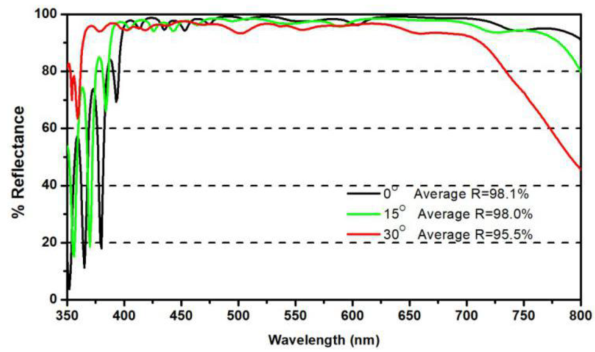
The first broadband HR coating studied was a typical application in virtual reality or augmented reality devices. The reflective spectrum was 400–700 nm, and the incident angle was 0°–30°. The thin film formula is very simple, which can be expressed as PMMA Substrate/(
HL)
5 1.3(
HL)
51.7(
HL)
5/Air.
H and
L represent the high and low refractive index deposition material, respectively. Using a simplex optimization process, we could get a smoother reflectance curve. When
H was TiO
2 and
L was SiO
2, we got a design result as shown in
Figure 3. The three lines with different colors represent the reflectance when the incident angle was 0°, 15°, and 30°. The average reflectance at different incident angles was greater than 96.3%. If the
H and
L materials are changed, the thin film only needs to get re-optimized to get roughly the same reflectance result.
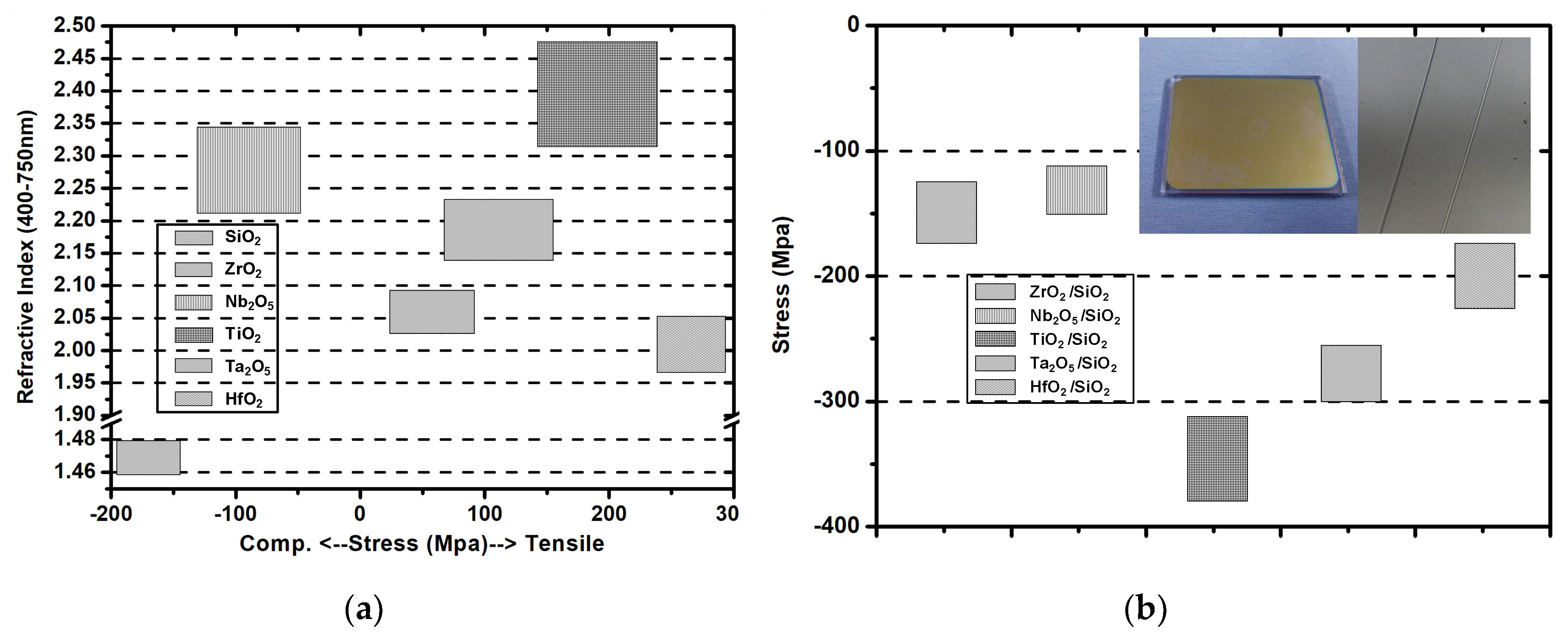
For the design of the coatings on PMMA, there were three concepts explored in our study. The high refractive index material must be carefully selected to reduce the stress property. Silicon oxide was preferred as a low refractive index material for its stability and process repeatability. Minimum thickness and layer number leads to the shortest deposition time and temperature rise. For choosing the
H material of the broadband HR coating, two series of experiments are carried out. First, we prepared single-layer coating samples of different materials, including SiO
2, TiO
2, Ta
2O
5, ZrO
2, HfO
2, and Nb
2O
5, as shown in
Figure 4a. The coating substrates were φ50 mm × 3 mm PMMA. For processes using different materials, deposition parameters were kept as consistent as possible, including deposition rate, heating temperature, ion source power, sample spatial location, and oxygen partial pressure. Evaporation rates were all 0.3 nm/s; the background vacuum was 9.0 × 10
−4 Pa; the heating temperature was 220 °C; the voltage and current of the RF (radio frequency) ion source were 1100 V and 1000 mA, respectively; the sample was 1.3 m in height above the electronic gun; coating vacuum after oxygenation was 2.0 × 10
−2 Pa; and the coating thickness was 300 nm. By measuring the changes in the substrate curvature before and after coating, the coating stress could be calculated by using the Stoney equation below [
21,
22,
23].
Es and
Vs are the modulus of elasticity and Poisson’s ratio of the PMMA substrate, respectively. They are obtained using the hardness test of PMMA. Besides,
ts and
tf are the thickness of the substrate and coating, respectively.
R is the radius of the curvature of the PMMA substrate. Through the measurement and calculation of different samples, we got the data of the refractive index and coating stress, as shown in the
Figure 4a. Stress changing was caused by multiple test measurement results.
In the same way, 30-layer HR coating samples of different
H materials were prepared. The results are shown in
Figure 4b. The biggest challenge for HR coating on PMMA is the stress problem. When the deposition material and process parameter were not fine enough, coatings always exhibited the crack or fall off phenomenon. Many test samples showed a cracking of the film layer. As the micrograph shows in
Figure 4b, although the HR coating layer did not fall off directly, many cracks inside the coating appeared. Unlike single-layer films, the stress development of multilayer films involves the combination of thermal parameters of various thin film materials and the rational matching of multiple interfaces, which is a more complicated process. Through a comprehensive evaluation of the HR coating samples, it was found that the Nb
2O
5 and SiO
2 combination has a better performance with regards to a lower probability of film rupture. Additionally, it should be noted that the coating stress result of different samples is a range but not a constant value in
Figure 4. This was mainly caused by the errors measured in multiple experiments and the temperature differences of the film formation area of different samples.
The problem of coating stress on PMMA will invalidate many previous methods. PMMA can only withstand temperatures up to 80 °C and cannot be subjected to high temperature annealing to remove residual stress. In addition, the temperature was controlled as much as possible during the coating process, and the electron beam or ion beam themselves had a heating effect. Therefore, at the beginning of the experiment, the heating method was not used and the coating was started at room temperature. It should also be noted that, since the coating process was a continuous heating process, the effect of temperature change on the refractive index and stress accumulation effect of the material should be considered.
After determining the selected coating material by adjusting the material evaporation rate and ion beam source parameter, we obtained the optimized deposition parameters. The highest deposition temperature was controlled to be less than 80 °C. Finally, the HR coating on the PMMA with no obvious defect was prepared successfully, and the process repeatability and stability were very good. The measured reflectance data is shown in
Figure 5a. The average reflectance is 95.5% at 30°, which has a 0.8% reduction compared with the design. This is explained by the fact that the deposition process was started at room temperature but the whole process temperature kept rising. The refractive index of the deposition material was not steady and some absorption also led to reflectance reduction. Based on interferometer measurement, the surface roughness RMS (Root Mean Square) of this as-deposited HR coating sample was less than 1/20λ, as shown in
Figure 5b.
We also conducted an environmental durability test. The test was carried out using dry heat at 80 °C, cold at −20 °C, and heat for 72 h at 80 °C and 80% relative humidity. In comparing the samples before and after the test, there is no obvious difference in outlook and reflectance, as shown in
Figure 6a. On the other hand, we used K-space test equipment to measure the stress distribution of samples with different deposition rates. The lowest average stress measured was −85 MPa at a 0.2 nm/s deposition rate, as shown in
Figure 6b. When deposition rates rose to 0.3 nm/s, the average stress of the HR coating increased to −165 MPa. Samples with different deposition rates also experienced environmental testing, and the deposition rate did not affect coating durability.
As we have been emphasizing, multi-layer coating stress is a complex model, which can be significantly influenced by lots of deposition parameters. Besides the deposition rate, temperature, spatial structure size, and oxygen partial pressure are likewise key parameters. We found that with different oxygen partial pressures, the composition of niobium oxide will be obviously changed. This will directly impact the extinction coefficient (
k) of niobium oxide, light absorption, and coating stress. In
Figure 7a, we can see the strong dependence of the extinction coefficient on oxygen partial pressure. From the comparison of the 30-layer HR coating samples of Nb
2O
5 and Nb
2O
x, both have excellent surface appearance and film quality. The measured reflectance of HR coating deposited at 1.0 × 10
−3 Pa can be observed as the red line in
Figure 7b. Its coating stress distribution and surface shape marked as the Nb
2O
x-1# are shown on the top, with mean values of −32 MPa and 0.018λ, respectively. For the regrettable absorption of niobium oxide, the averaged reflectance from 400–700 nm had a 4% reduction compared with the HR coating mentioned before, as demonstrated by the black line in
Figure 7b. Based on the method of regulating oxygen partial pressure, we successfully prepared a broadband HR coating, which has an average 98.5% reflectance from 750 to 1550 nm, as the green line shows in
Figure 7b. The oxygen partial pressure was set at 0.5 × 10
−3 Pa. The coating stress distribution and surface shape marked as the Nb
2O
x-2# are shown below, with mean values of −45 MPa and 0.04λ, respectively. The total thickness of this broadband HR coating was 7.7 μm. For such a thick coating on PMMA, the sample showed no obvious appearance defect and good environmental durability. After being repeatedly pulled by tape CT-24, the broadband HR coating exhibited a good adhesion performance.

 ,
, 


