1. Introduction
The low temperature polycrystalline silicon thin film transistor (poly-Si TFT) fabricated on glass substrates has been widely studied and used for active-matrix organic liquid crystal display (AMOLCD) and active matrix organic light emitting (AMOLED) display applications, peripheral driver and pixel switches circuits [
1], because it has a high electron mobility and On-state current when compared to the amorphous silicon (a-Si) TFT [
2]. The most critical issue for the conventional poly-Si TFT is its high drain electric field (DEF) that causes a great deal of impact ionization, which leads to an intense kink effect and degrades the device performance [
3,
4]. This drawback also limits this device’s use in digital and analog circuits on glass for high resolution displays. Moreover, the conventional poly-Si device encounters a large leakage current problem that degrades its switching performance [
5].
Many structures have been reported to be able to reduce the high DEF and thus to improve the device characteristics [
3,
6,
7,
8,
9,
10]. The offset-gate device was shown to lower the DEF effectively, but its On-current was also significantly decreased because of an additional series resistance [
6]. Lightly doped drain (LDD) [
7], RSD [
8,
9], and GOLDD [
10] were proposed to reduce the series resistance problem. Even though the above mentioned structures could effectively lower the high DEF, the ON-current of those structures still need to be improved when considering the current driving capability and high-resolution display applications. In addition, most RSD structures need to adopt chemical mechanical polishing (CMP) processes [
9]. Therefore, to implement a low DEF device with a reduced leakage current and an improved operation current structure at the same time is a very important issue for designing a high performance poly-Si TFT.
A DG structure was used to improve the device current drive capability effectively [
11,
12]. However, the double gate structure has an electric field superposition problem around the channel/drain junction and worsens the DEF [
13]. Moreover, the fabrication of this structure has a misalignment issue between the up and bottom gates [
14]. In addition, the leakage current at the OFF state mode for the double-gate structure becomes unacceptably large [
13]. A DG TFT with a conventional RSD structure was designed to improve the device performance [
13,
14,
15]. But these designs required two CMP process steps, and the precise wet etching on the nitride sacrificial layer is difficult to control. Our previously study proposed a Z-gate structure to overcome the electric field superposition problem [
16], but it still encountered a misalignment problem between the top and bottom gates.
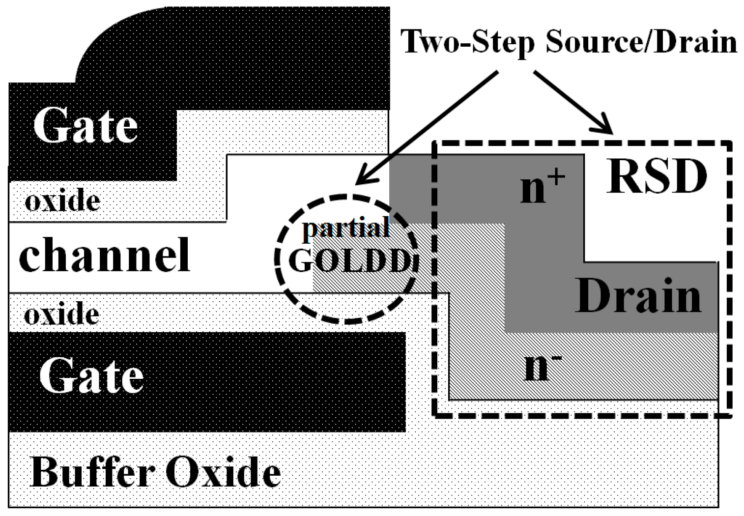
In this work, we proposed a DG TFT together with a TSD structure (DGTSD-TFT) to improve the device characteristics. This TSD design can be an extended RSD (E-RSD) and form a partial thicker channel near the drain to lower the impact of the electric field superposition problem [
16]. There is a report that two-dimensional drain TFTs can reduce the device leakage current because of a lower lateral electric field by changing its highest location [
17]. But the LDD area shown in [
17] is difficult to control after adopting two different kinds of dopants. The TSD design can form a partial gate overlapped lightly doped drain (P-GOLDD) that is similar to the structure shown in [
17], to further lower the lateral electric field. The design information of DGTSD-TFT is shown in
Figure 1. The DG is adopted to improve the device ON-state current. The E-RSD and P-GOLDD used in TSD can overcome the extra high electric field in conventional DG devices. Because we combine the RSD and DG designs in our device, we need one more mask, as compared to the conventional RSD or DG devices, to accomplish our structure. This DGTSD-TFT can effectively lower the high DEF, and alleviate the impact ionization phenomenon to repress the device kink effect. Moreover, this P-GOLDD design ensures that the top and bottom channels are not a symmetric frame; the channel length is defined by the top one, which makes DGTSD-TFTs free of the misalignment problem.
2. Device Fabrication
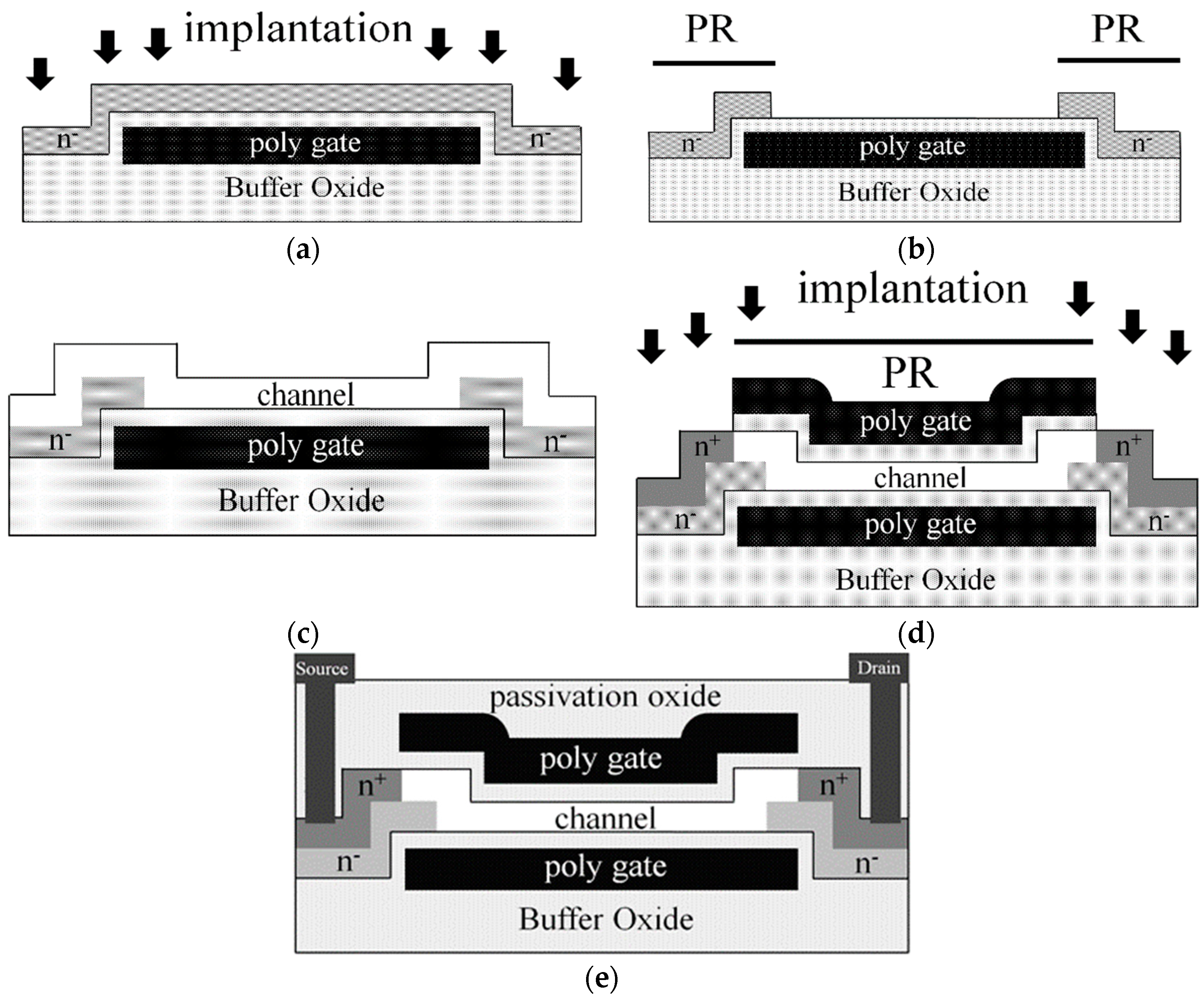
To fabricate the device, an n
+ poly-Si layer (200 nm) was first formed on oxidized silicon wafers, and this layer was then patterned to be the bottom gate. After that, an oxide (50 nm) and an undoped α-Si (200 nm) were deposited. A phosphorous ion implantation (dose = 1 × 10
13 cm
−2 at 40 keV) was used, and a GOLDD area was defined.
Figure 2 illustrates the main process steps of a DGTSD-TFT. An undoped α-Si with 100 nm thickness was formed, after which the active area was patterned. Thereafter, this α-Si channel layer was recrystallized in a furnace for 24 h at 600 °C to become the poly-Si film. Then, a top gate oxide (50 nm) and an n
+ poly-Si top gate (200 nm) were in turn deposited. After patterning the top gate region, a phosphorous implantation was performed to make the drain and source regions. Subsequently, a 0.2 μm oxide was formed to serve as the passivation layer. Finally, contact areas were opened and an Al-Si-Cu metal layer was accomplished and defined to be the metal pads afterward. Further improved device characteristics can be achieved by applying an H
2 or NH
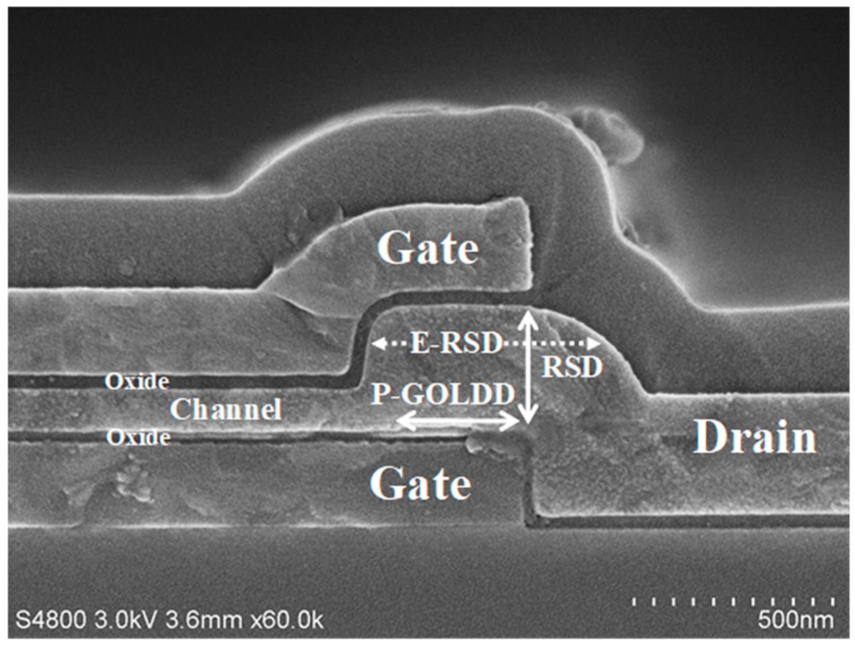
3 treatment. The scanning electron microscopy (SEM) photography for our DGTSD-TFT with a 0.5-μm P-GOLDD region and a 300 nm RSD structure is shown in
Figure 3.
3. Structure Simulation, Device Measurement and Discussion
In order to investigate the reduction of the DEF and impact ionization rate (IPR) in DGTSD-TFT compared to a single top gate traditional device, two dimensional device numerical simulations were adopted by using the ISE-TCAD simulator [
3,
18]. Analyzing the location and magnitude of high DEF, which can be simulated using the simulation methodology in our previous work [
16], can validate the improvement of DEF with the proposed structure. Since the kink effect is caused by a great deal of impact ionization, we can also achieve a suppressed kink effect device by designing a low IPR structure [
3]. Furthermore, the device leakage current can be predicted by simulating the device DEF with a negative gate bias [
9]. From the simulation results (simulated at
Vds = 10 V and
Vgs = 5 V), the maximum DEF and IPR are 2.51 × 10
5 V/cm and 3.72 × 10
27 cm
−3/s for our DGTSD structure, respectively, and those numbers are 3.59 × 10
5 V/cm and 2.73 × 10
28 cm
−3/s for an STG traditional device. If a traditional DG TFT is modeled, these values are much higher than those in an STG device because of the DG superposition effect [
16]. The detailed simulation comparisons for convention STG and DG devices can be found in our previous publication [
16]. A negative gate bias was simulated to predict the devices’ leakage characteristics. The simulated maximum DEF (
Vgs = −5 V and
Vds = 5 V) is 4.48 × 10
5 V/cm for our DGTSD design and 7.07 × 10
5 V/cm for a conventional structure. The reduced DEF and IPR in DGTSD-TFT will be beneficial for lowering the device leakage current and mitigating the kink phenomenon even when a DG structure is used. Moreover, the operation current of our proposed device is increased.
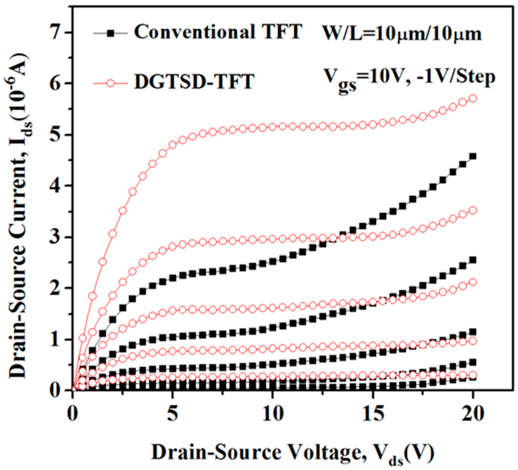
Figure 4 depicts the measured output
Vds-
Ids curves for a DGTSD-TFT and for an STG traditional device. The On-state current of DGTSD-TFT is about twice as large as that of the STG traditional structure. It is obvious that the kink effect of our DGTSD-TFT can be overcome and repressed effectively by virtue of the design of the P-GOLDD and E-RSD structure (two-step source/drain design). These designed structures are very helpful in decreasing the TFT high DEF problem and in improving the device performance.
The measured transfer performance of DGTSD-TFT and a conventional top single gate structure are shown in
Figure 5. It can be seen that the leakage current, which is measured at
Vgs = −5 V and
Vds = 5 V, of the DGTSD-TFT (5.12 × 10
−11 A) is lower than that of the traditional STG TFT (3.47 × 10
−10 A). This low leakage current is contributed by a low negative gate bias DEF that comes from a two-step source/drain design. Our P-GOLDD design is a two-dimensional drain doping profiles structure, which can provide a way to manipulate the location and physical extent of the high electric field near the drain [
17]. In addition, our extended RSD design can form a partial thicker channel near the drain to lower the impact of the electric field superposition problem [
16]. Therefore, the high DEF can be reduced and moved away from the gate electrode to lower the leakage current [
17]. The threshold voltage of the proposed TFT and conventional TFT is 5.5 and 6 V (extracted at
Vds = 0.1 V as
Ids = 10 nA), respectively. The measured subthreshold swing (S.S.) and effective mobility (μ
eff) of DGTSD-TFT (conventional STG device) is 0.65 (1.34) V/dec and 20.07 (9.33) cm
2/V·s, at
Vds = 0.1 V. These improvements are attributed to the double gate design. The calculated ON/OFF current ratios of our proposal DGTSD structure and of the conventional one are 2.84 × 10
6 and 3.34 × 10
5, respectively. The device breakdown voltages (
VBR), defined as the drain voltage when
Ids = 2 nA at
Vgs = 0 V [
3], of the proposed TFT and conventional STG TFT, are 12.93 and 8.97 V, respectively. These improvements are attributed to the reduced DEF structures.
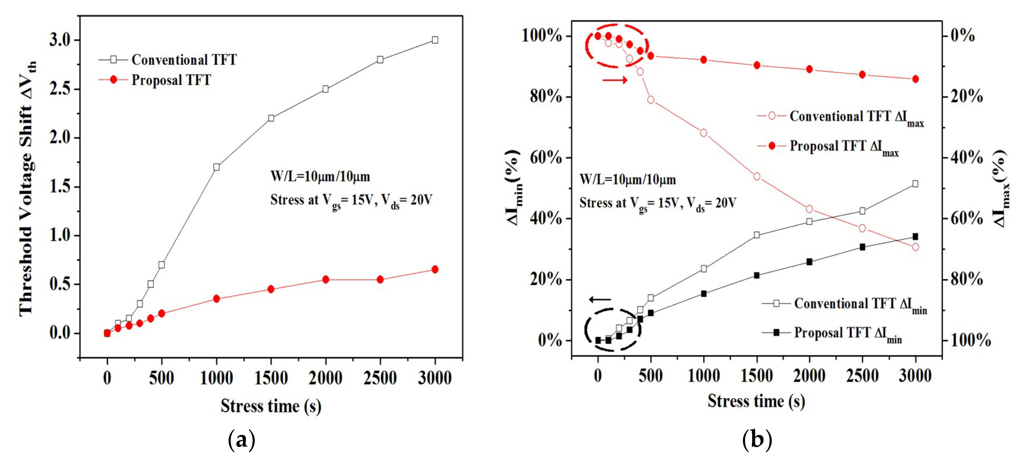
A 3000 s hot-carrier stress test for both structures was performed at
Vds = 20 V and
Vgs = 15 V to investigate the devices’ electrical reliability.
Figure 6a depicts the shift of threshold voltage (
Vth) for both devices after stress. The
Vth of the STG traditional device after the reliability test changes significantly, but it remains almost the same value in our DGTSD-TFT.
Figure 6b demonstrates that the current variations of the maximum ON-current drop (Δ
Imax) and minimum drain current increase (Δ
Imin) after the reliability stress. It can be observed that the Δ
Imax and Δ
Imin for the STG traditional device exhibit bigger changes than those of our DGTSD-TFT after the 3000 s hot carrier test. The Δ
Imax and Δ
Imin are 14.2% and 34.1% for our DGTSD-TFT, respectively, while those numbers are 51.4% and 69.4% for the conventional STG device. The reliability test indicates that our designed E-RSD and P-GOLDD structures are beneficial for achieving a reliable device.
These experimental results show that the proposed double-gate accompanied with the two-step source/drain design can increase the device’s operation current and lower its drain electric field as compared with a traditional STG structure. Additionally, the proposed device’s OFF-state leakage current can be reduced, and no profound kink effect is observed. In addition, the proposed structure has no misalignment problem that is commonly encountered in traditional DG devices [
13].

 ,
, 