Contamination Particles and Plasma Etching Behavior of Atmospheric Plasma Sprayed Y2O3 and YF3 Coatings under NF3 Plasma

Abstract
:1. Introduction
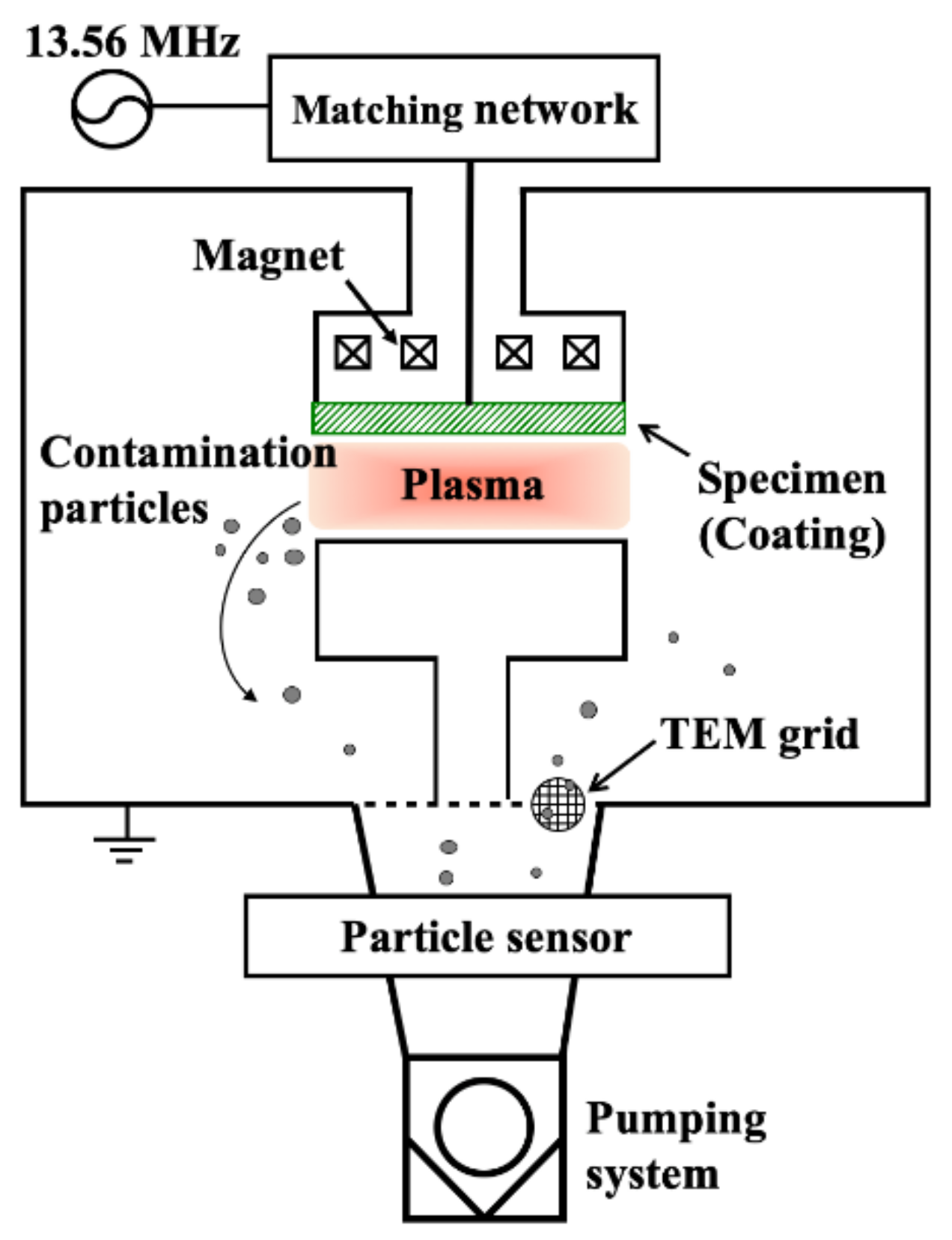
2. Experimental
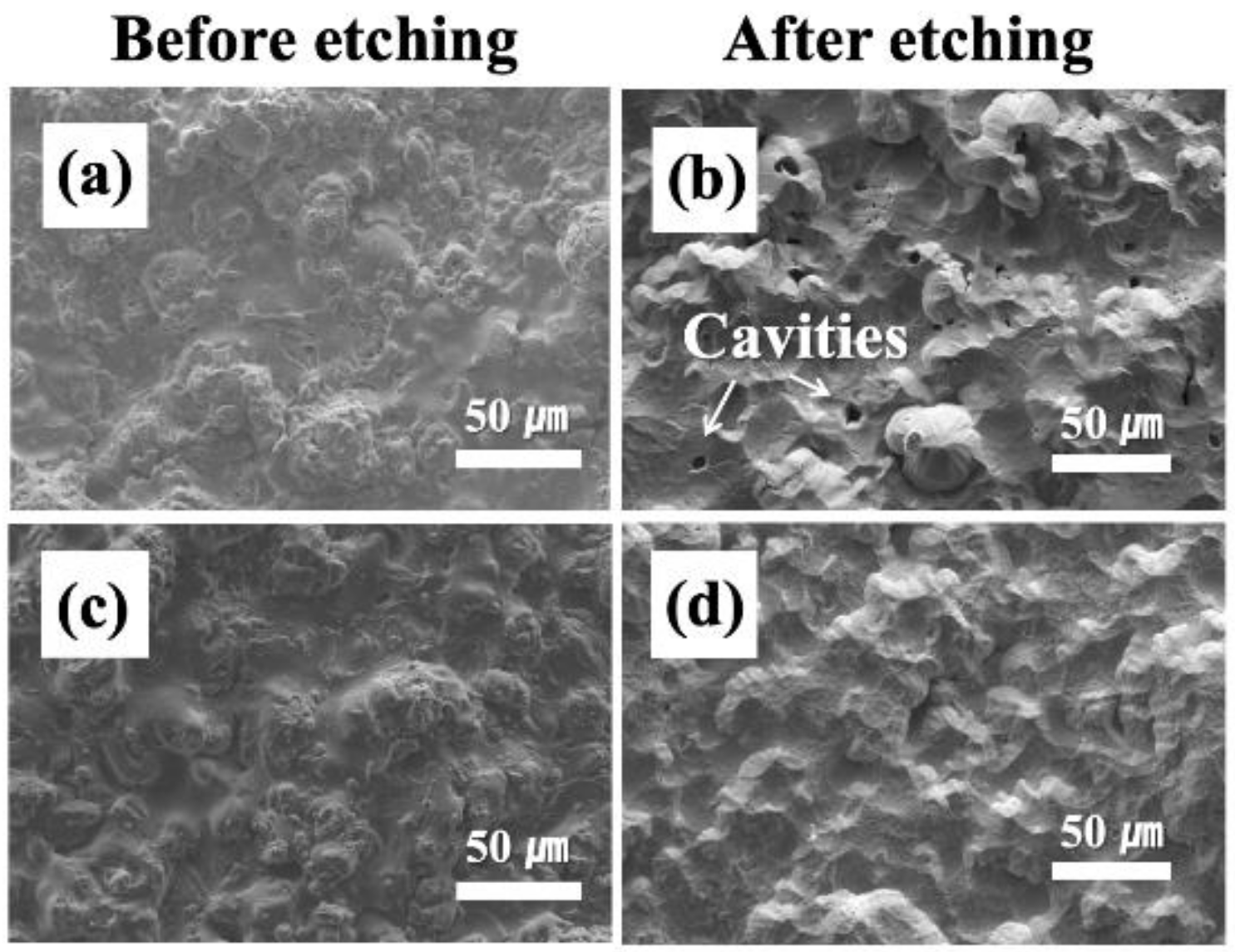
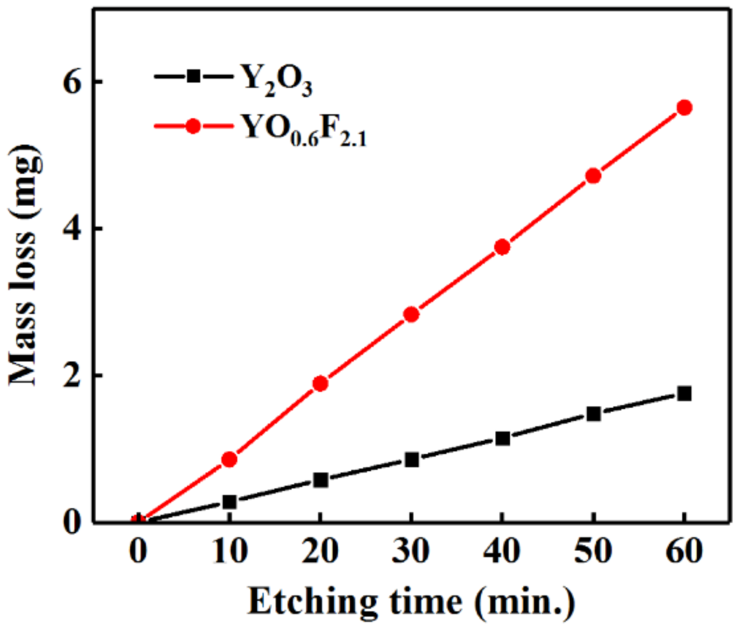
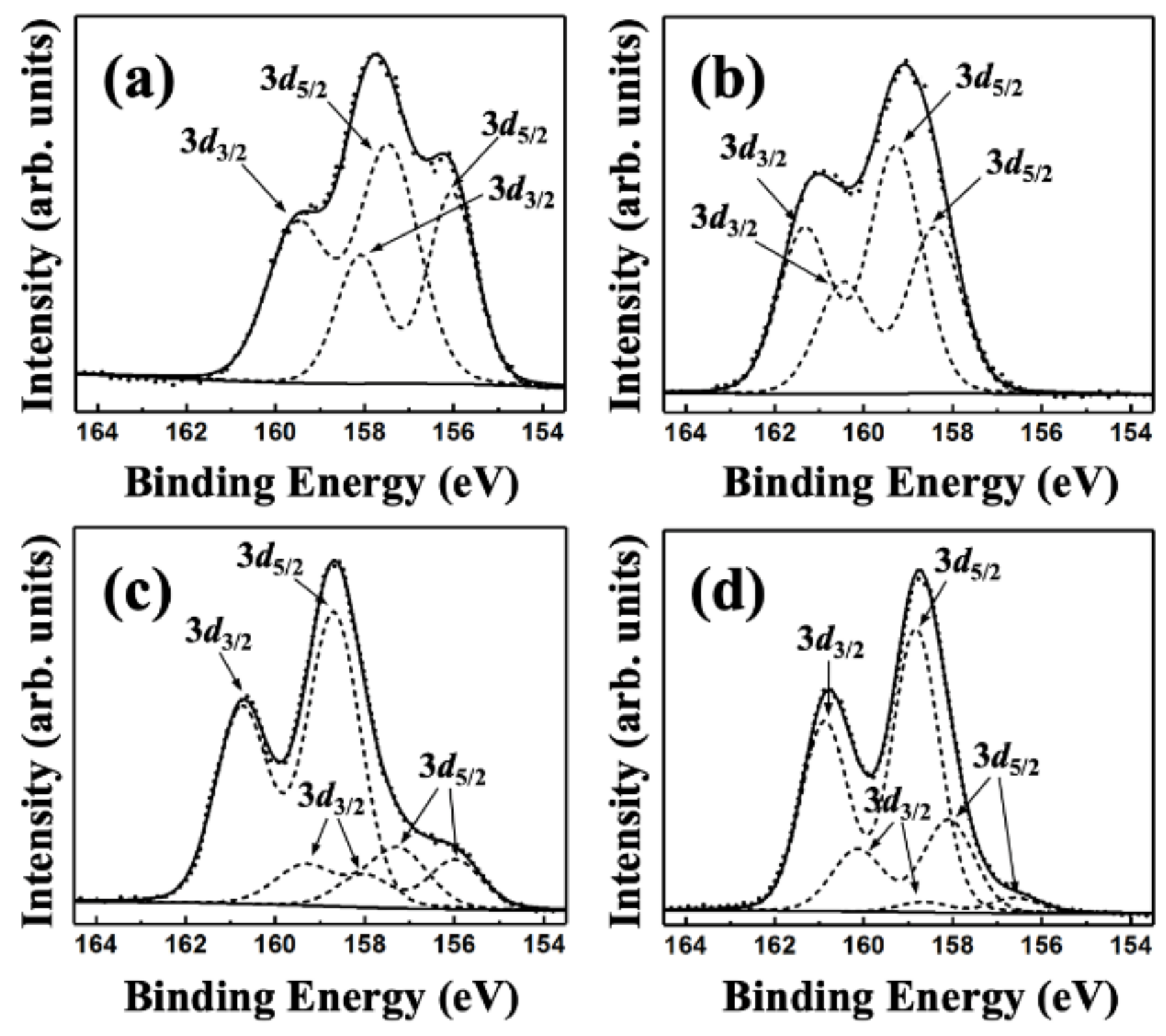
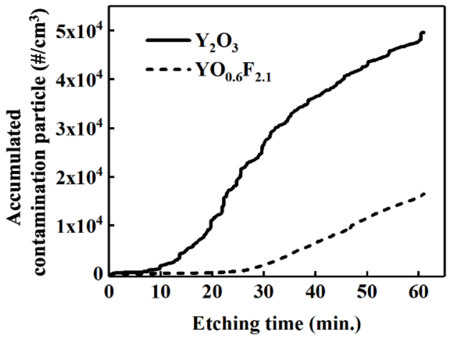
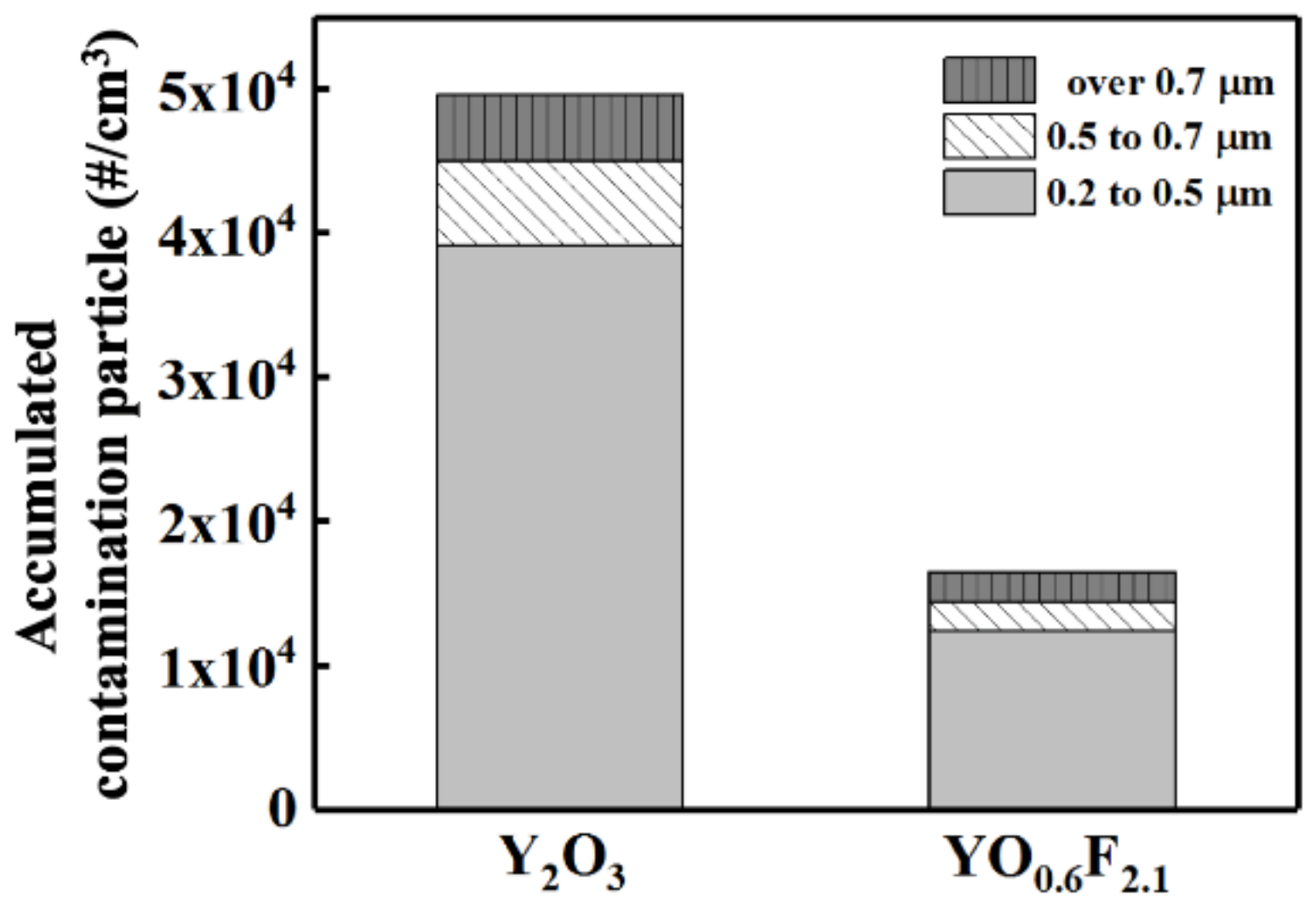
3. Results and Discussion
4. Conclusions
Author Contributions
Funding
Conflicts of Interest
References
- Coburn, J.W.; Winters, H.F. Plasma etching-A discussion of mechanisms. J. Vac. Sci. Technol. 1979, 16, 391–403. [Google Scholar] [CrossRef]
- Donnelly, V.M.; Kornblit, A. Plasma etching: Yesterday, today, and tomorrow. J. Vac. Sci. Technol. A Vac. Surf. Films 2013, 31, 050825. [Google Scholar] [CrossRef]
- Abe, H.; Yoneda, M.; Fujiwara, N. Developments of plasma etching technology for fabricating semiconductor devices. Jpn. J. Appl. Phys. 2008, 47, 1435. [Google Scholar] [CrossRef]
- Ito, N.; Moriya, T.; Uesugi, F.; Matsumoto, M.; Liu, S.; Kitayama, Y. Reduction of particle contamination in plasma-etching equipment by dehydration of chamber Wall. Jpn. J. Appl. Phys. 2008, 47, 3630. [Google Scholar] [CrossRef]
- Kasashima, Y.; Natsuko, N.; Uesugi, F. Instantaneous generation of many flaked particles by impulsive force of electric field stress acting on inner wall of mass-production plasma etching equipment. Jpn. J. Appl. Phys. 2013, 52, 066201. [Google Scholar] [CrossRef]
- Babaeva, N.Y.; Kushner, M.J. Ion energy and angular distributions into the wafer-focus ring gap in capacitively coupled discharges. J. Phys. D Appl. Phys. 2008, 41, 062004. [Google Scholar] [CrossRef]
- Sung, D.; Jeong, S.; Park, Y.; Volynets, V.N.; Ushakov, A.G.; Kim, G.H. Effect on plasma and etch-rate uniformity of controlled phase shift between rf voltages applied to powered electrodes in a triode capacitively coupled plasma reactor. J. Vac. Sci. Technol. A Vac. Surf. Films 2009, 27, 0734. [Google Scholar] [CrossRef]
- Yang, Y.; Kushner, M.J. Modeling of dual frequency capacitively coupled plasma sources utilizing a full-wave Maxwell solver: I. Scaling with high frequency. Plasma Sources Sci. Technol. 2010, 19, 055011. [Google Scholar] [CrossRef]
- Yang, Y.; Kushner, M.J. Modeling of dual frequency capacitively coupled plasma sources utilizing a full-wave Maxwell solver: II. Scaling with pressure, power and electronegativity. Plasma Sources Sci. Technol. 2010, 19, 055012. [Google Scholar] [CrossRef]
- Schulze, J.; Schungel, E.; Donko, Z.; Czarnetzki, U. Charge dynamics in capacitively coupled radio frequency discharges. J. Phys. D Appl. Phys. 2010, 43, 225201. [Google Scholar] [CrossRef]
- Machima, P.; Hershkowitz, N. SiO2 and Si3N4 etch mechanisms in NF3/hydrocarbon plasma. J. Phys. D Appl. Phys. 2006, 39, 673. [Google Scholar] [CrossRef]
- Ji, B.; Yang, J.H.; Badowski, P.R.; Karwacki, E.J. Optimization and analysis of NF3 in situ chamber cleaning plasmas. J. Appl. Phys. 2004, 95, 4452–4462. [Google Scholar] [CrossRef]
- Kastenmeir, B.E.E.; Matsuo, P.J.; Oehrlein, G.S.; Langan, J.G. Remote plasma etching of silicon nitride and silicon dioxide using NF3/O2 gas mixtures. J. Vac. Sci. Technol. A Vas. Surf. Films 1998, 16, 2047–2056. [Google Scholar] [CrossRef]
- Matsuo, P.J.; Kastenmeier, B.E.E.; Oehrlein, G.S.; Langan, J.G. Silicon etching in NF3/O2 remote microwave plasmas. J. Vac. Sci. Technol. A Vas. Surf. Films 1999, 17, 2431–2434. [Google Scholar] [CrossRef]
- Shin, J.S.; Kim, M.; Song, J.B.; Jeong, N.G.; Kim, J.T.; Yun, J.Y. Fluorine plasma corrosion resistance of anodic oxide film depending on electrolyte temperature. Appl. Sci. Converg. Technol. 2018, 27, 9–13. [Google Scholar]
- Zhao, D.; Wang, C.Y.; Chen, Y.; Wang, Y.G. Phase composition, structural, and plasma erosion properties of ceramic coating prepared by suspension plasma spraying. Int. J. Appl. Ceram. Technol. 2018, 15, 1388–1396. [Google Scholar] [CrossRef]
- Cao, Y.C.; Zhao, L.; Luo, J.; Wang, K.; Zhang, B.P.; Tokota, H.; Ito, Y.; Li, J.F. Plasma etching behavior of Y2O3 ceramics: Comparative study with Al2O3. Appl. Surf. Sci. 2016, 366, 304–309. [Google Scholar] [CrossRef]
- Song, J.B.; Kim, J.T.; Oh, S.G.; Shin, J.S.; Chun, J.R.; Yun, J.Y. Effect of sealing time of anodic aluminum oxide (AAO) film for preventing plasma damage. Sci. Adv. Mater. 2015, 7, 127–132. [Google Scholar] [CrossRef]
- Goto, T.; Sugawa, S. Observation of sputtering of yttrium form Y2O3 ceramics by low-energy Ar, Kr, and Xe ion bombardment in microwave-excited plasma. Jpn. J. Appl. Phys. 2015, 54, 128003. [Google Scholar] [CrossRef]
- Kim, D.M.; Lee, S.H.; Alexander, W.B.; Kim, K.B.; Oh, Y.S.; Lee, S.M. X-Ray photoelectron spectroscopy study on the interaction of yttrium-aluminum oxide with fluorine-based plasma. J. Am. Ceram. Soc. 2011, 94, 3455–3459. [Google Scholar] [CrossRef]
- Choi, H.; Kim, K.; Choi, H.; Kang, S.; Yun, J.; Shin, Y.; Kim, T. Plasma resistant aluminum oxide coatings for semiconductor processing apparatus by atmospheric aerosol spray method. Surf. Coat. Technol. 2010, 205, S125–S128. [Google Scholar] [CrossRef]
- Erkmen, Z.E.; Anghaie, S. Interaction of yttria with uranium fluoride gases (UFn, n = 4, 6) at high temperatures. J. Am. Ceram. Soc. 1994, 77, 1624–1632. [Google Scholar] [CrossRef]
- Tahara, R.; Tsunoura, T.; Yoshida, K.; Yano, T.; Kishi, Y. Fabrication of dense yttrium oxyfluoride ceramics by hot pressing and their mechanical, thermal, and electrical properties. Jpn. J. Appl. Phys. 2018, 57, 06JF04. [Google Scholar] [CrossRef]
- Lin, T.K.; Wuu, D.S.; Huang, S.Y.; Wang, W.K. Preparation and characterization of sprayed-yttrium oxyfluoride corrosion protective coating for plasma process chambers. Coatings 2018, 8, 373. [Google Scholar] [CrossRef]
- Wang, W.K.; Lin, Y.X.; Xu, Y.J. Structural and fluorine plasma etching behavior of sputter-deposition yttrium fluoride film. Nanomaterials 2018, 8, 936. [Google Scholar] [CrossRef] [PubMed]
- Ma, T.; List, T.; Donnelly, V.M. Comparisons of NF3 plasma-cleaned Y2O3, YOF, and YF3 chamber coatings during silicon etching in Cl2 plasmas. J. Vac. Sci. Technol. A Vac. Surf. Films 2018, 36, 0734. [Google Scholar] [CrossRef]
- Shiba, Y.; Teramoto, A.; Goto, T.; Kishi, Y.; Shirai, Y.; Sugawa, S. Stable yttrium oxyfluoride used in plasma process chamber. J. Vac. Sci. Technol. A Vac. Surf. Films 2017, 35, 021405. [Google Scholar] [CrossRef]
- Kim, D.M.; Jang, M.R.; Oh, Y.S.; Kim, S.; Lee, S.M.; Lee, S.H. Relative sputtering rates of oxides and fluorides of aluminum and yttrium. Surf. Coat. Technol. 2017, 309, 694–697. [Google Scholar] [CrossRef]
- Lin, T.K.; Wang, W.K.; Huang, S.Y.; Tasi, C.T.; Wuu, D.S. Comparison of erosion behavior and particle contamination in mass-production CF4/O2 plasma chambers using Y2O3 and YF3 protective coatings. Nanomaterials 2017, 7, 183. [Google Scholar] [CrossRef]
- Kim, D.M.; Oh, Y.S.; Kim, S.; Kim, H.T.; Lim, D.S.; Lee, S.M. The erosion behaviors of Y2O3 and YF3 coatings under fluorocarbon plasma. Thin Solid Films 2011, 519, 6698–6702. [Google Scholar] [CrossRef]
- Lin, T.K.; Wuu, D.S.; Huang, S.Y.; Wang, W.K. Characteristics of yttrium fluoride and yttrium oxide coating for plasma process equipment prepared by atmospheric plasma spraying. Jpn. J. Appl. Phys. 2016, 55, 126201. [Google Scholar] [CrossRef]
- Bakan, E.; VaBen, R. Ceramic top coats of plasma-sprayed thermal barrier coatings: Materials, processes, and properties. J. Therm. Spray Technol. 2017, 26, 992–1010. [Google Scholar] [CrossRef]
- Fan, W.; Bai, Y. Review of suspension and solution precursor plasma sprayed thermal barrier coatings. Ceram. Intern. 2016, 42, 14299–14312. [Google Scholar] [CrossRef]
- Pawlowski, L. The Science and Engineering of Thermal Spray Coatings; John Wiley & Sons: Chichester, UK, 2008. [Google Scholar]
- Miyashita, H.; Kikuchi, T.; Kawasaki, Y.; Katakura, Y.; Ohsako, N. Particle measurements in vacuum tools by in situ particle monitor. J. Vac. Sci. Technol. A Vac. Surf. Films 1999, 17, 1066–1070. [Google Scholar] [CrossRef]
- Hulst, H.C. Light Scattering by Small Particles; Courier Publications, Inc.: New York, NY, USA, 1981. [Google Scholar]
- NIST X-ray Photoelectron Spectroscopy Database. Available online: https://srdata.nist.gov/xps/ (accessed on 15 September 2012).


| Compound Content (at.%) | Y2O3 Coating | YO0.6F2.1 Coating | ||
|---|---|---|---|---|
| Before Etching | After Etching | Before Etching | After Etching | |
| Yttrium (Y3d) | 28.3 | 29.2 | 26.9 | 27.3 |
| Oxygen (O1s) | 70.3 | 15.0 | 16.8 | 11.8 |
| Fluorine (F1s) | 1.4 | 55.8 | 56.3 | 60.9 |
| Compound Content (wt.%) | Particle Generated in Y2O3 Coating | Particle Generated in YO0.6F2.1 Coating |
|---|---|---|
| Yttrium | 63.5 | 61.8 |
| Oxygen | 0.8 | 0.6 |
| Fluorine | 35.7 | 37.6 |
© 2019 by the authors. Licensee MDPI, Basel, Switzerland. This article is an open access article distributed under the terms and conditions of the Creative Commons Attribution (CC BY) license (http://creativecommons.org/licenses/by/4.0/).
Share and Cite
Song, J.-B.; Kim, J.-T.; Oh, S.-G.; Yun, J.-Y. Contamination Particles and Plasma Etching Behavior of Atmospheric Plasma Sprayed Y2O3 and YF3 Coatings under NF3 Plasma. Coatings 2019, 9, 102. https://doi.org/10.3390/coatings9020102
Song J-B, Kim J-T, Oh S-G, Yun J-Y. Contamination Particles and Plasma Etching Behavior of Atmospheric Plasma Sprayed Y2O3 and YF3 Coatings under NF3 Plasma. Coatings. 2019; 9(2):102. https://doi.org/10.3390/coatings9020102
Chicago/Turabian StyleSong, Je-Boem, Jin-Tae Kim, Seong-Geun Oh, and Ju-Young Yun. 2019. "Contamination Particles and Plasma Etching Behavior of Atmospheric Plasma Sprayed Y2O3 and YF3 Coatings under NF3 Plasma" Coatings 9, no. 2: 102. https://doi.org/10.3390/coatings9020102
APA StyleSong, J.-B., Kim, J.-T., Oh, S.-G., & Yun, J.-Y. (2019). Contamination Particles and Plasma Etching Behavior of Atmospheric Plasma Sprayed Y2O3 and YF3 Coatings under NF3 Plasma. Coatings, 9(2), 102. https://doi.org/10.3390/coatings9020102