1. Introduction
Optical monitoring techniques can be applied in the production of optical coatings in almost all deposition plants. Both commercial and homemade optical monitoring devices are widely used all over the world, and choosing a good optical monitoring strategy is a key issue for the production of high-quality optical coatings. There is a great variety of optical monitoring techniques, and they are divided into monochromatic and broadband techniques [
1]. In the case of monochromatic techniques, the question of having a proper monitoring strategy was raised many decades ago. The most impressive example of this was the production of narrow band-pass filters using turning point optical monitoring [
2,
3,
4]. The production of very complicated optical filters became possible due to the presence of a very strong error self-compensation effect associated with this type of monitoring. The physics of the error self-compensation effect was explained many years later [
5], and it was shown that the advantage of turning point monitoring appears only in the case of filters with resonant filter cavities. For other types of optical coatings, monochromatic-level monitoring was proposed many years ago in various forms [
6,
7,
8,
9]. For monochromatic-level monitoring, the choice of monitoring strategy is usually decided by the specifications of monitoring wavelengths and signal termination levels or swing [
10] termination levels for all coating layers. The choice of monochromatic monitoring strategy is not a straightforward task, and recent efforts have been made to automate this choice [
11,
12].
In the case of broadband monitoring, various monitoring strategies are also possible. The first alternative is the choice between direct and indirect monitoring strategies [
1,
10]. The main advantage of direct monitoring was indicated by Macleod [
7]. In this case, we monitor one of the samples that we want to produce. Unfortunately, direct broadband monitoring can lead to the development of a strong, cumulative effect of thickness error growth. This effect was even noticed in the first works done on broadband monitoring [
13,
14] and was later investigated in detail [
15]. Indirect broadband monitoring allows one to use several monitoring chips and, thus, prevent the fast growth of thickness errors. However, with this type of monitoring, we lose the previously noted advantage of direct monitoring. The recent progress in monitoring hardware arrangements [
16,
17] allows one to combine the advantages of direct and indirect monitoring. In the arrangement reported in these works, the monitor holder has several monitoring chips and is located on the main wheel of the deposition chamber with the same radial position as those of the deposited samples. Thus, the cumulative effect of thickness errors can be reduced by using several monitoring chips during the coating deposition.
The negative cumulative effect of thickness error growth is connected with the correlation of thickness errors by optical monitoring procedures [
15]. Although, the correlation of errors can also lead to a positive effect of self-compensation of influence of errors in various layer thicknesses. In the case of broadband monitoring, this effect was first noticed four decades ago [
13,
14]. However, a comprehensive study of the error self-compensation effect associated with direct broadband monitoring began only recently, after the presence of a very strong effect was detected in the production of Brewster’s angle polarizers for high-fluence optics [
18]. The mathematical investigation of the error self-compensation mechanism in the case of broadband monitoring was performed in Ref. [
19]. The results of this investigation were formulated in terms of singular values of rectangular matrices describing the correlation of errors in the course of broadband monitoring. Unfortunately, this form of representation is not convenient for practical applications, and the degree of correlation between the thickness errors and the strength of the error self-compensation effect can be calculated using computational experiments on optical coating production simulations [
20,
21].
The recent progress in broadband monitoring hardware [
16,
17] allows one to apply different direct monitoring strategies. In particular, direct broadband monitoring can be performed using several monitoring chips. It is also possible to remove monitoring chips and bring them back to the measurement position many times during the coating deposition. This strategy was previously applied in the case of indirect broadband monitoring, and it was shown that it had a certain advantage in monitoring some types of optical coatings [
22].
Despite the obvious progress in monitoring arrangement, choosing the optimal strategy in the case of broadband monitoring is still an open question. When studying this question, we should take into account the negative and positive effects connected with the correlation of thickness errors. On the one hand, the use of several monitoring chips prevents rapid development of the cumulative effect of thickness errors. On the other hand, it can also reduce the degree of correlation of thickness errors and the associated positive effect of error self-compensation. The goal of this paper is to present a computational approach that can be applied for the comparison of various monitoring strategies while also taking into account the above-mentioned effects. We hope that such a comparison will be useful in practice to help select the optimal monitoring strategy for a given coating design.
2. The Computational Approach to Assessing the Degree of Thickness Error Correlation and the Strength of the Error Self-Compensation Effect
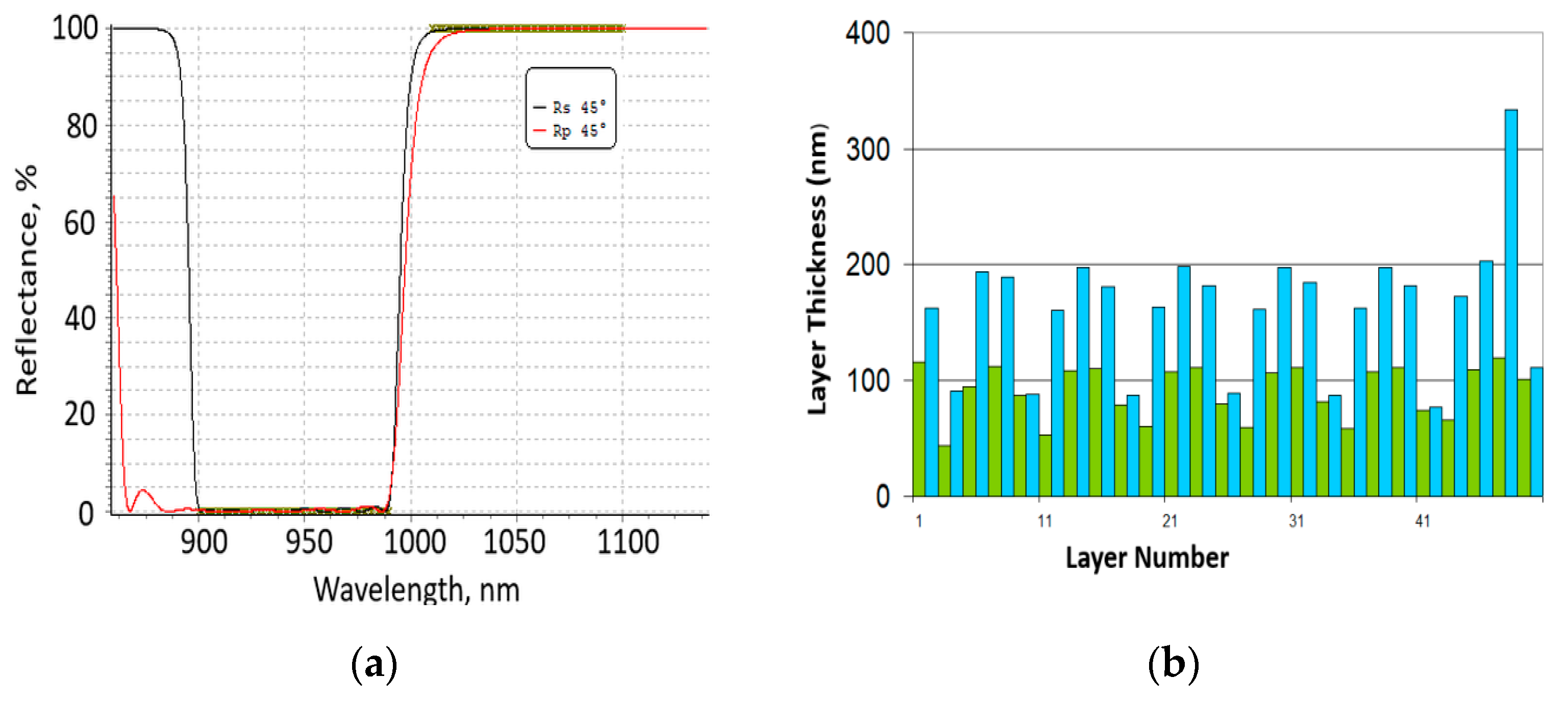
To illustrate the proposed computational approach, we analyzed a design of 50-layer, nonpolarizing edge filter with a 45° light incidence. Its theoretical spectral characteristics and layer physical thicknesses are presented in
Figure 1. The filter used model high- and low- index materials with refractive indices of 2.35 and 1.45 (for example, model TiO
2 and SiO
2 indices). The first layer counting from the substrate was the high-index material layer, and the substrate refractive index was 1.52. It was designed using OptiLayer thin film software (v12.12) [
23]. Computational manufacturing experiments with this filter [
24] demonstrated the presence of a strong error self-compensation effect in the case of broadband monitoring in the normal incidence transmittance mode.
Let
be physical thicknesses of a coating design. Here,
m is the total number of coating layers, and
m = 50 in the case of the considered nonpolarizing filter. In the course of production, actual layer thicknesses
differed from the planned values. Consider broadband monitoring using measured transmittance spectra. When using modern broadband monitoring devices, such spectra usually have hundreds or even thousands of spectral points. Let
d be the growing thickness of the
j-th coating layer. The measured transmittance is
Here, δTmeas is the error in measured transmittance data. In Equation (1) and the following equations, we omitted the indication of an obvious dependence on wavelength λ.
With broadband monitoring, the deposition of the
j-th layer is terminated in accordance with the condition that the minimum is reached by the discrepancy function
Here, the summation is carried out over the wavelength grid at which the transmittance is measured.
It follows from Equation (2) that the actual thickness of the deposited j-th layer is associated not only with the errors in transmittance data but is also determined by the actual thicknesses of all previously deposited layers. This is the reason for the correlation of errors in layer thicknesses.
As outlined above, a rigorous mathematical investigation of the correlation of thickness errors was provided in [
19]. To present the main result of this investigation, we introduced the vector of thickness errors
. When considering Equation (2) for all coating layers, starting from layer
j = 2, the following matrix appears:
Here, are partial derivatives of the intensity transmission coefficient for the subsystem of layers with the numbers from 1 to j.
Let
and
be eigenvalues and eigenvectors of the matrix Cj, and
be the elements of the eigenvectors
. With their help, the following raw vectors are introduced for all i from 1 to j and all j from 2 to m:
These raw vectors were then used to form the rectangular matrix
W with the dimensions
k ×
m, where
m is the number of coating layers, and
k = (
m − 1)/(
m + 2)/2. In accordance with the results of Ref. [
19], the correlation of thickness errors led to a small norm of the vector
WΔ. To formalize the concept of the smallness of this norm, the parameter α was introduced in [
20]. It is calculated as
Here, Δ0 is the normalized error vector Δ (i.e., ), and is the averaged square norm of the vectors WΔr over all vectors Δr with the norm .
The introduced parameter α compares the value of the norm WΔ0 with the average value of the norm WΔr for all random vectors of the unit length. The introduced parameter is called the degree of thickness error correlation. The smaller this parameter the stronger the correlation of errors.
In [
20,
21], the degree of thickness error correlation was estimated for two cases in which a strong error self-compensation effect was observed either practically [
18] or in the course of simulating the coating deposition [
24]. The Brewster’s angle polarizer and the nonpolarizing edge filter were considered here. In both cases, the smallness of parameter α was confirmed. We consider the related results for the edge filter later in this document.
Subsequently, we proceeded to assess the strength of the error self-compensation effect. Despite the correlation of thickness errors, error vectors Δ are also random in nature since they are determined by various random factors. Therefore, the estimation of the strength of the error self-compensation effect should have a statistical form. Since this effect is caused by the correlation of thickness errors, it is also natural to estimate it by comparing it with the influence of uncorrelated thickness errors.
To assess the impact of errors on coating spectral characteristics, we used the merit function to solve the respective design problem. In the case of the nonpolarizing edge filter, it has the form
Here, Ts and Tp are transmittances for the s- and p-polarized light at 45° light incidence; is the target transmittance, equal to 0% in the 900–990 nm spectral band and equal to 100% in the 1010–1100 nm band; and L is the total number of spectral grid points that has the step of 1 nm in the two target spectral bands.
Let us designate δMF(Δ) as the deviation of merit function corresponding to the error vector Δ. We wanted to compare the deviations that are caused by the correlated and uncorrelated thickness errors.
The uncorrelated thickness errors are most consistent with stable production processes using time and quartz crystal monitoring. It is generally accepted that when using these monitoring techniques, the best accuracy in controlling layer thicknesses is about 1% of the planned thickness values. Let us denote as the root-mean-square value of merit function deviations calculated for the large number of random error vectors Δ that are set so their coordinates Δdj are distributed according to Gaussian law with zero mathematical expectations and standard deviations equal to 1% of the thicknesses of the corresponding layers. Thus, is an estimate of the effect of uncorrelated errors. Further, to obtain this estimate, we generated 1 million uncorrelated error vectors.
To obtain the vector of correlated thickness errors, one can use computational manufacturing experiments to simulate the deposition process with broadband optical monitoring. In [
24], OptiLayer software [
23] was used for this purpose. In [
21], a simplified simulator of this process was proposed that, on the one hand, fully reflected the process of thickness error correlation and, on the other hand, allowed error vectors to be generated much faster than full simulators of the deposition processes. In this paper, we applied the simplified simulator from [
21].
In order to evaluate the strength of the error self-compensation effect
S, two possible assessments were considered in our previous works [
20,
25]. They were also based on a comparison of the effect of correlated and uncorrelated thickness errors. In Ref. [
20], a special
Dα region was considered in the unit sphere in the space of error vectors, and an estimate for parameter
S was introduced using all correlated error vectors with a degree of correlation of thickness errors less than α. In Ref. [
25], an estimate for
S was introduced with the normalization of all error vectors to unit norm vectors. Here, we introduce a new evaluation form for
S, which we hope is more consistent with practice.
Depending on the levels of simulated error factors, generated error vectors Δ will have various norms. In general, with a lower norm of the error vector, lower values of the merit function variations should be expected. For a more objective comparison of correlated and uncorrelated thickness errors, it is advisable to consider, in both cases, error vectors of the same norm. For this reason, we normalized all correlated errors vectors so that their norms were 1% of the design vector norm. With this normalization, the strength of the error self-compensation effect for a specific vector of correlated errors will be estimated as
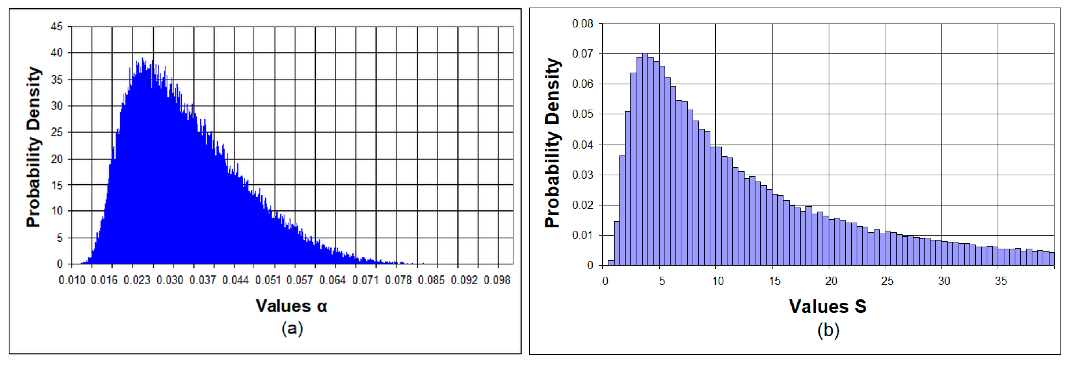
Figure 2 shows the probability density functions of the distributions of the degree of correlation of thickness errors and the strength of the error self-compensation effect in the case of direct transmittance monitoring in the 450–950 nm spectral band. These distributions are calculated using 1,000,000 vectors of correlated errors.
In full accordance with previously obtained results [
18,
24],
Figure 2 demonstrates the smallness of parameter α. At the same time, almost all calculated
S values were large enough, which indicates the presence of a strong error self-compensation effect. The average
S value was equal to 16.6.
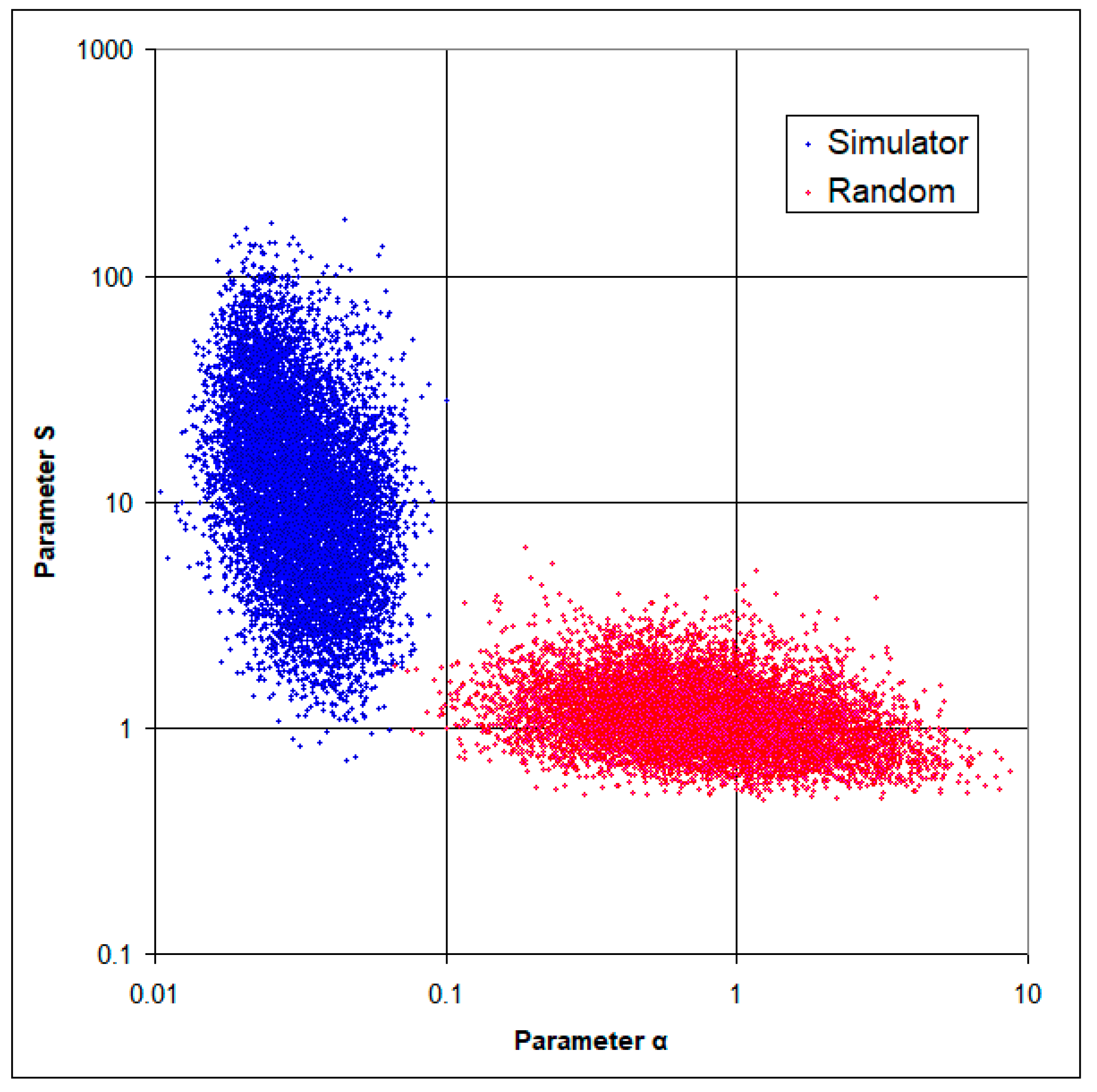
An even more visual representation of a strong correlation of thickness errors and the associated error self-compensation effect is given by
Figure 3, where pairs of α and
S values are presented for correlated and uncorrelated error vectors. The pairs of values corresponding to these two types of errors are located in significantly different parts of the (α,
S) plane.
3. Comparison of Various Monitoring Strategies
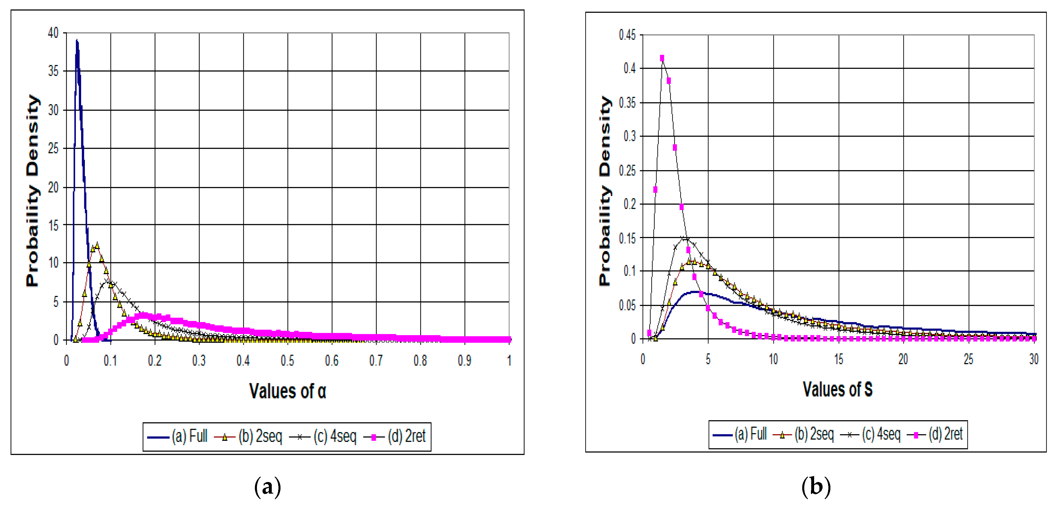
In this section, we used the estimates of the previous section to compare four different monitoring strategies. The first one was the direct monitoring strategy with all filter layers monitored using one of the samples to be produced. The next strategy used two subsequent monitoring chips, so that filter layers with the numbers from 1–24 were monitored using the first chip, and layers 25–50 were monitored using the second chip. The third strategy applied four monitoring chips that were used to monitor layers 1–12, 13–24, 25–36, and 37–50. The fourth strategy used two chips that were moved out of the measurement position and returned back to this position so that the first chip monitored layers 1, 2, 4, …, 50, while the second chip monitored layers 3, 5, …, 49. Monitoring the first two layers with a single chip allowed us to increase the optical contrast for monitoring low-index layers (even layers) by applying the first high-index layer to this chip. All four strategies caused correlation of thickness errors, but we expected that, in the first case, parameter α would have lower values than in the other cases. Recall that parameter α is smaller when the correlation of errors is higher.
In all four cases, 1,000,000 error vectors were generated to calculate α and
S values.
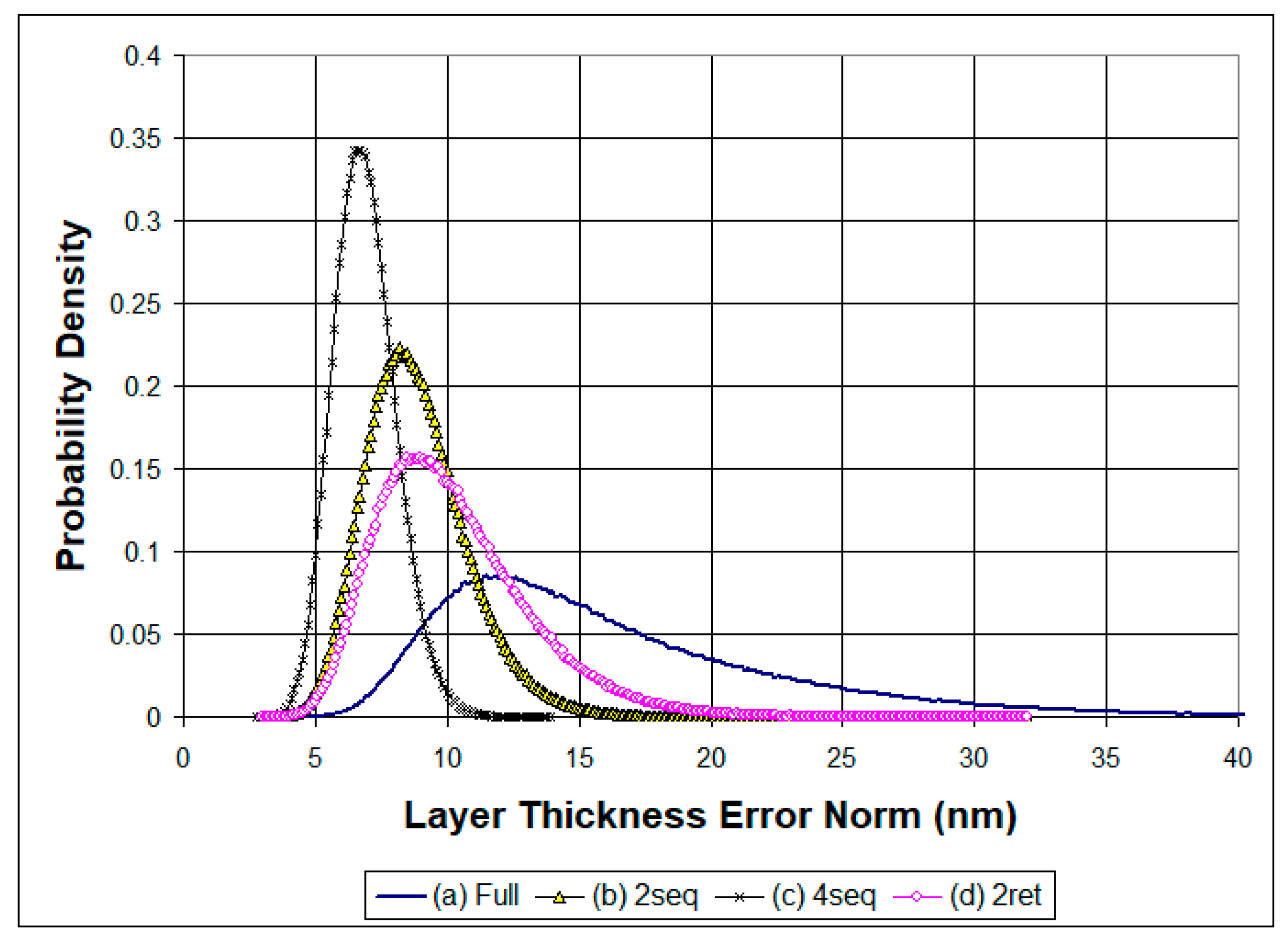
Figure 4 shows the probability density functions for the degree of thickness error correlation α and the strength of the error self-compensation effect
S.As one may expect, parameter α had lower values in the case of direct monitoring. This reflects a stronger correlation of thickness errors when all layer thicknesses are monitored using a single sample. In the case of direct monitoring, the average S value was the largest, and it was equal to 16.6.
For predictive comparisons of various monitoring strategies, we also needed to compare thickness error levels for all four cases. Recall that for the comparison with uncorrelated errors, all error vectors in Equation (7) were normalized to the same value. Following this, strategies with several monitoring chips were introduced to reduce thickness error levels.
Figure 5 shows the probability density functions of the distributions of norms of error vectors for the considered strategies. As before, calculations were performed based on 1,000,000 simulation tests in each case.
Indeed, levels of thickness errors were noticeably reduced when the strategies with several monitoring chips were applied. The average values of error vector norms in
Figure 5 were equal to 17.25 nm in the case of direct monitoring and 9.32, 6.92, and 10.55 nm in the cases of strategies with several monitoring chips.
Despite somewhat weaker error self-compensation effects, the strategies with several monitoring chips may be preferable because of the lower levels of thickness errors. To evaluate a positive effect of error self-compensation, taking into account the expected levels of thickness errors, we made the following considerations. From a theoretical point of view, in the first approximation, the deviation
δMF(Δ) grew linearly with an increase in the norm of the error vector Δ. The strength of the error self-compensation effect
S was estimated by Equation (7) for the error vectors Δ with the norms equal to 0.01
D, where
D is the norm of the design vector. Let us denote as
the average values of the error vector norms in the distributions shown in
Figure 5. Using these average values, we introduced the effective strength of the error self-compensation effect for a given monitoring strategy by the equation
Table 1 compares average
S values in
Figure 4b, average
in
Figure 5, and
Seff values for the considered four monitoring strategies.
The discussion of the obtained results is provided in the next section.
4. Discussion
Recent achievements in the development of broadband monitoring hardware allow one to combine advantages of direct and indirect monitoring strategies through the use of several monitoring chips that are located on the main wheel of the deposition chamber. Even more, it is also possible to remove monitoring chips and bring them back to the measurement position many times during the coating deposition. This opens a way for using various broadband monitoring strategies. Thus, the question of comparing various strategies and choosing the most appropriate one becomes important. The presented research outlines a way for answering this question.
When considering optical monitoring strategies, we should take into account the correlation of thickness errors by optical monitoring procedures. This correlation causes both negative and positive effects. On one hand, it can lead to the development of a strong cumulative effect of thickness error growth, but on the other hand, it can result in the self-compensation of thickness errors. In this paper, we proposed a computational approach to assess the degree of thickness error correlation and the strength of the error self-compensation effect. The proposed approach was used to compare four strategies of broadband monitoring. It was shown that in the case of a 50-layer, nonpolarizing edge filter, the direct monitoring strategy provided the strongest correlation of thickness errors and the strongest error self-compensation effect. At the same time, in this case, one should expect the highest level of thickness errors caused by the negative cumulative effect of error growth. This reduces the effective strength of the error self-compensation effect. In the case of monitoring strategies with two and four subsequent monitoring chips, the strength of the error self-compensation effect was lower, but the expected levels of thickness errors were also lower. To evaluate the combined effect caused by the correlation of thickness errors, the effective strength of the error self-compensation effect
Seff was introduced by Equation (8).
Table 1 shows that, in the case of strategies with several subsequent monitoring chips,
Seff was a bit higher than in the case of direct monitoring. However, taking into account the approximate nature of statistical estimates, on this basis, one should not conclude that the strategies with several subsequent chips have an absolute advantage in the case of a nonpolarizing edge filter. In the case of this design, all of the first three strategies deserve attention.
As for the fourth considered strategy, in the case of the nonpolarizing edge filter, it was clearly less suitable than the first three. However, this does not mean that the fourth strategy cannot be the best option for other designs. It is worth noting that the advantage of this strategy was discovered earlier [
22] for a design with layers that were essentially thinner than the layers of the discussed filter.
The presented computational approach to comparing various broadband monitoring strategies is general and can be applied to check the prospects of the production of various types of optical coatings.


