Article

The Effect of Cathodic Arc Guiding Magnetic Field on the Growth of (Ti0.36Al0.64)N Coatings

1
Department of Physics, Chemistry and Biology, Linköping University, SE-581 83 Linköping, Sweden
2
Department of Materials Science and Engineering, D3.3 Saarland University, D-66123 Saarbrücken, Germany
3
Seco Tools AB, SE-737 82 Fagersta, Sweden
4
Institute Jean Lamour, Campus ARTEM, University of Lorraine, CNRS, F-54011 Nancy, France
5
Sandvik Coromant, SE-126 80 Stockholm, Sweden
*
Author to whom correspondence should be addressed.
Coatings 2019, 9(10), 660; https://doi.org/10.3390/coatings9100660
Submission received: 11 September 2019 / Revised: 1 October 2019 / Accepted: 10 October 2019 / Published: 12 October 2019

Abstract

:
We use a modified cathodic arc deposition technique, including an electromagnetic coil that introduces a magnetic field in the vicinity of the source, to study its influence on the growth of (Ti0.36Al0.64)N coatings. By increasing the strength of the magnetic field produced by the coil, the cathode arc spots are steered toward the edge of the cathode, and the electrons are guided to an annular anode surrounding the cathode. As a result, the plasma density between the cathode and substrate decreased, which was observed as a lateral spread of the plasma plume, and a reduction of the deposition rate. Optical emission spectroscopy shows reduced intensities of all recorded plasma species when the magnetic field is increased due to a lower number of collisions resulting in excitation. We note a charge-to-mass ratio decrease of 12% when the magnetic field is increased, which is likely caused by a reduced degree of gas phase ionization, mainly through a decrease in N2 ionization. (Ti0.36Al0.64)N coatings grown at different plasma densities show considerable variations in grain size and phase composition. Two growth modes were identified, resulting in coatings with (i) a fine-grained glassy cubic and wurtzite phase mixture when deposited with a weak magnetic field, and (ii) a coarse-grained columnar cubic phase with a strong magnetic field. The latter conditions result in lower energy flux to the coating’s growth front, which suppresses surface diffusion and favors the formation of c-(Ti,Al)N solid solutions over phase segregated c-TiN and w-AlN.

1. Introduction

(Ti,Al)N exhibits high hardness which, in combination with excellent corrosion and wear resistance properties, makes it a suitable tool coating material for a wide range of metal-cutting applications under harsh operating conditions [1,2,3,4]. Although the solubility of Al in TiN is very limited [5,6,7], the growth of metastable cubic B1 structured (c-(Ti,Al)N) solid solutions is possible under non-equilibrium conditions by, for example, physical vapor deposition techniques [7,8]. At elevated temperatures, solid solution c-(Ti,Al)N undergoes spinodal decomposition into coherent c-TiN or c-AlN rich domains [2]. The coherency strains and elastic property difference between c-TiN and c-AlN domains act as barriers for dislocation movement, resulting in age hardening [9,10,11] and improved mechanical coating properties while retaining a high oxidation resistance [2,3,8,12,13,14], which has been associated with the formation of a protective Al2O3/TiOx layer [15,16].
At even higher temperature, c-AlN transforms to a wurtzite (B4) structured w-AlN by a nucleation and growth mechanism [17], which is detrimental to the hardness and wear resistance of the coating [4,18,19]. Besides understanding the effects of temperature and pressure on phase stability [20,21,22], large efforts have been made to suppress the c-AlN to w-AlN phase transformation. Such efforts include the modification of coating architecture [23], the addition of alloying elements [24], and defect engineering [25].
It has been demonstrated that tuning of the plasma properties during growth by physical vapor deposition techniques can be used to control the growth of coatings and their corresponding properties. Greczynski et al. [26] reported the possibility of controlling the phase composition and hardness of (Ti,Al)N coatings by varying the ion-to-neutral ratios of Ti and Al species using a hybrid high-power impulse magnetron sputtering (HiPIMS)/magnetron deposition setup. Similarly, Mayrhofer et al. [27] observed variations in crystallographic orientation (texture) and hardness by regulation of the ion-to-Ti flux ratio in magnetron sputter deposition of (Ti,Al)N. Through a particular deposition setup, Andersson et al. [28] have shown that the applied magnetic field used to steer the arc on the cathode surface significantly influences the plasma ionization degree, the confinement of highly energetic electrons in front of the cathode, and the energy transfer of impinging species at the coating growth front.
The aim of this work is to investigate the influence of varying arc guiding magnetic field generated by an assembly of permanent magnets and an electromagnetic coil located behind the arc source on the cathode spot movement, plasma properties, and the growth of Ti0.36Al0.64N coatings. The deposited coatings were evaluated in terms of grain size, phase content, surface morphology, residual stress and hardness.

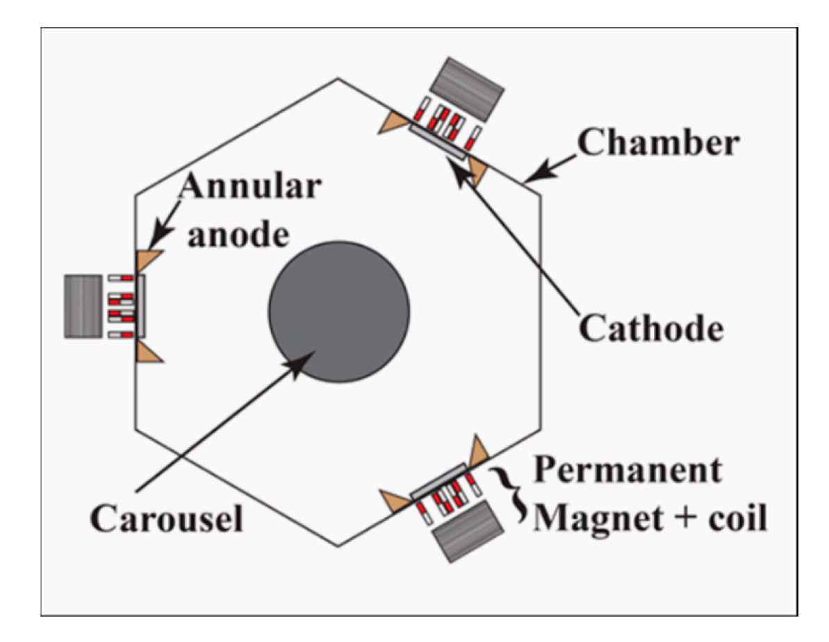
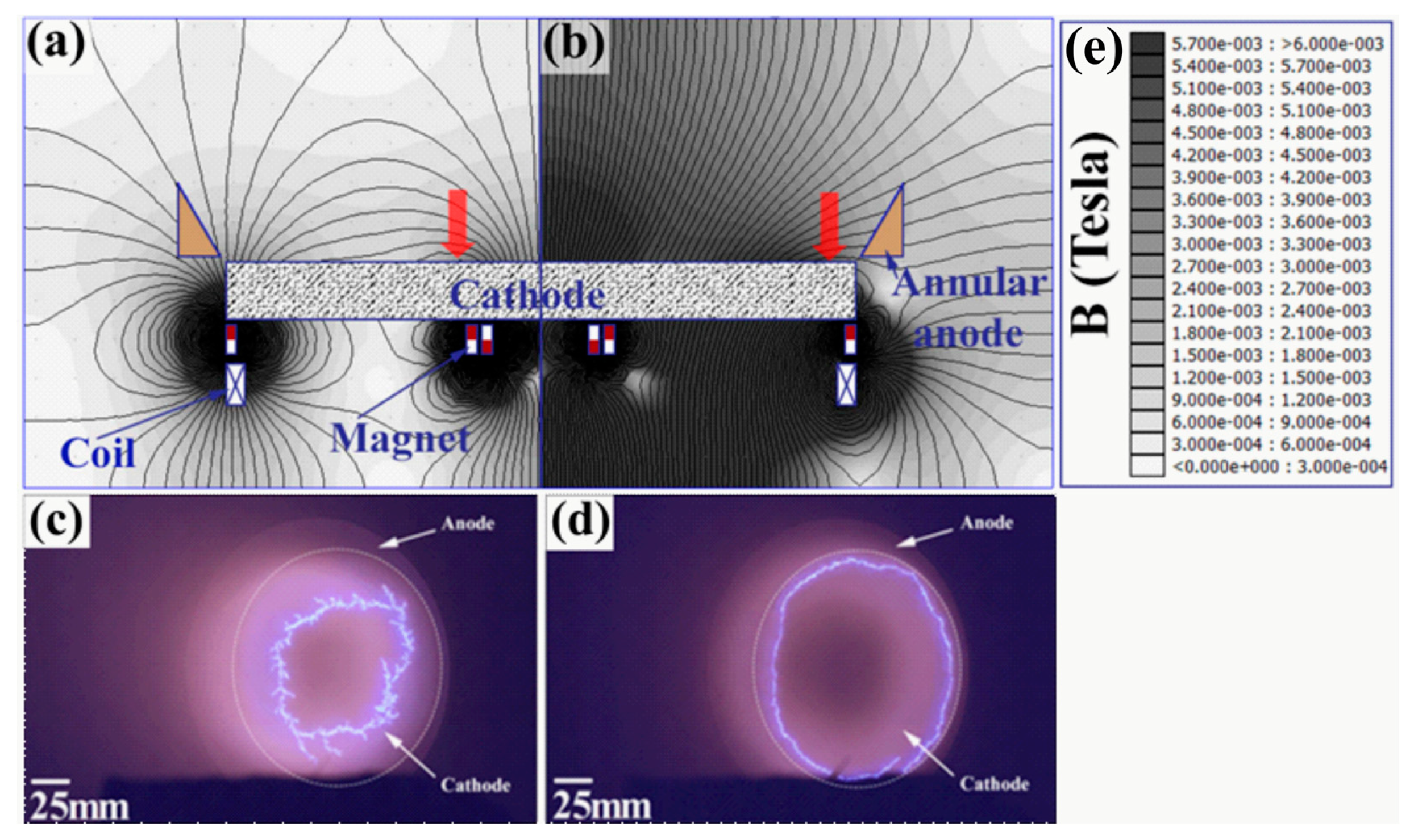
2. Materials and Methods
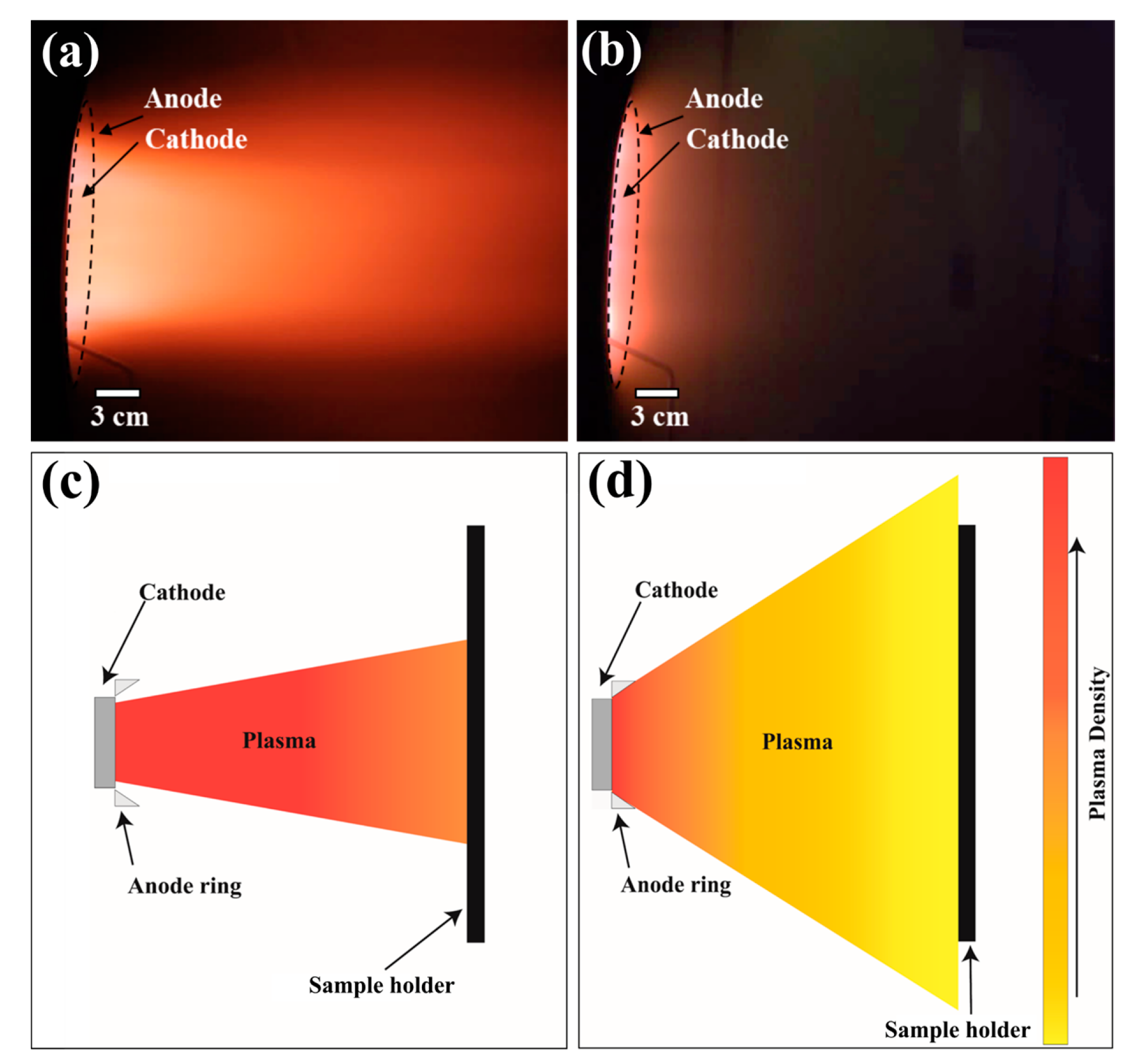
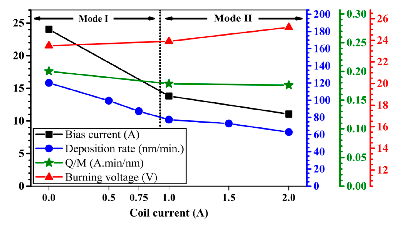
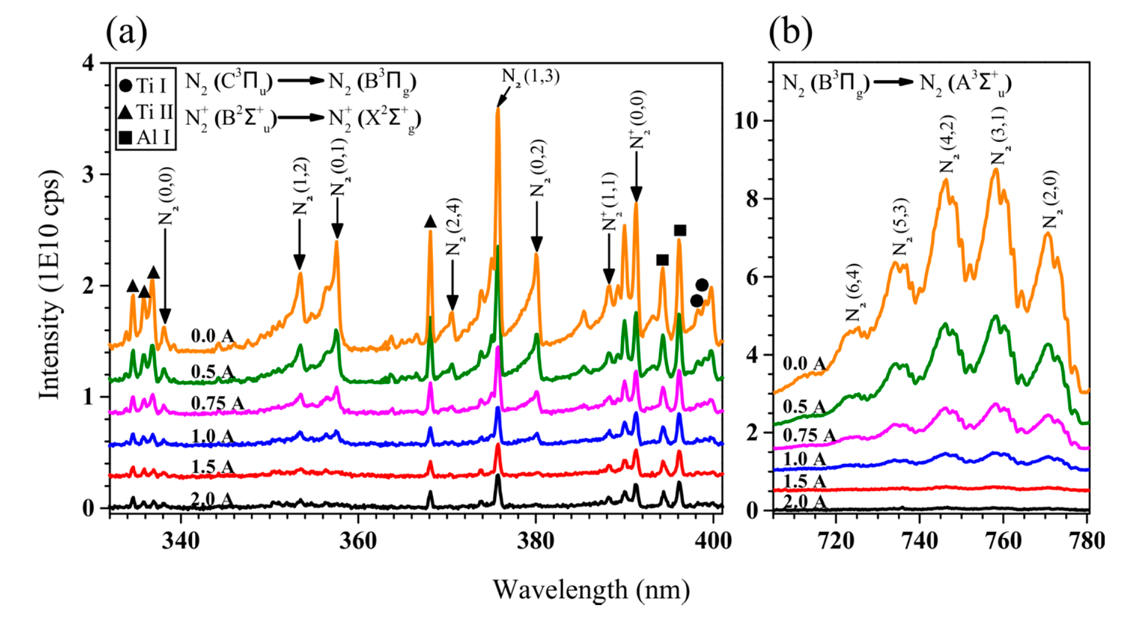
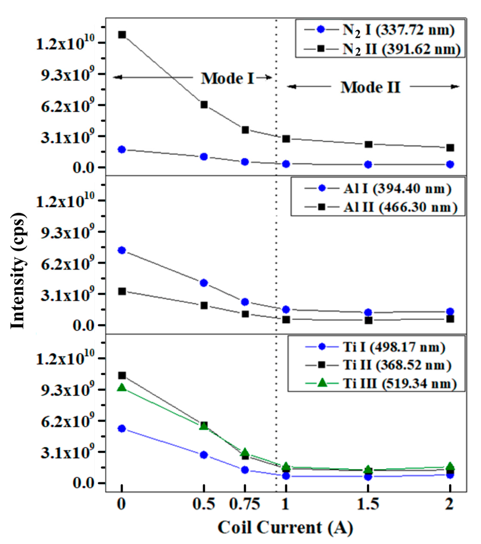
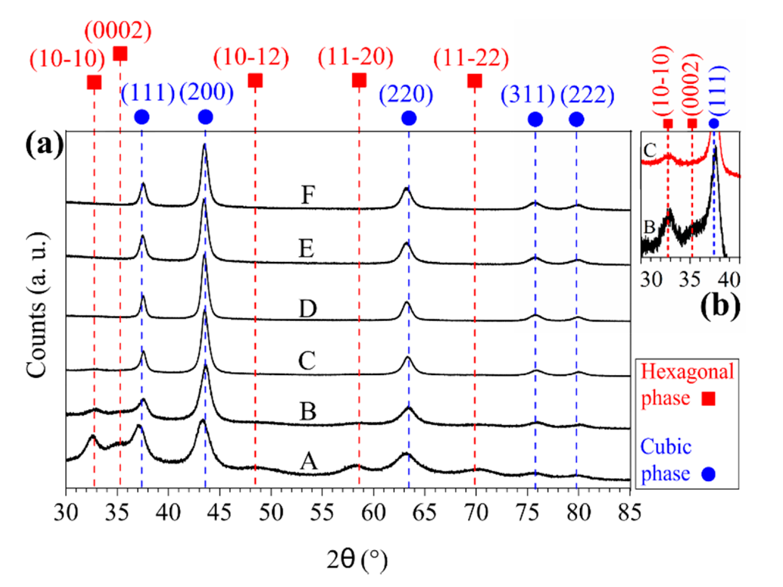
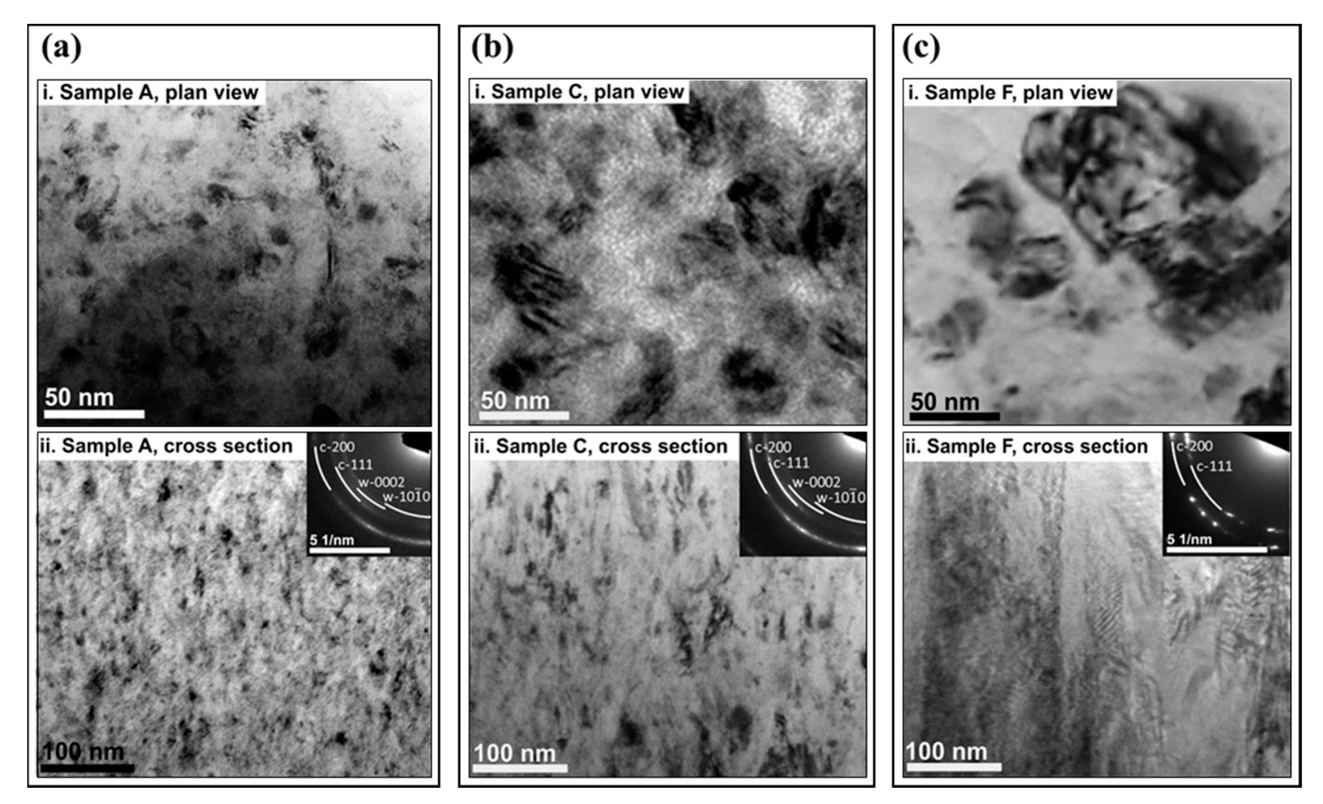
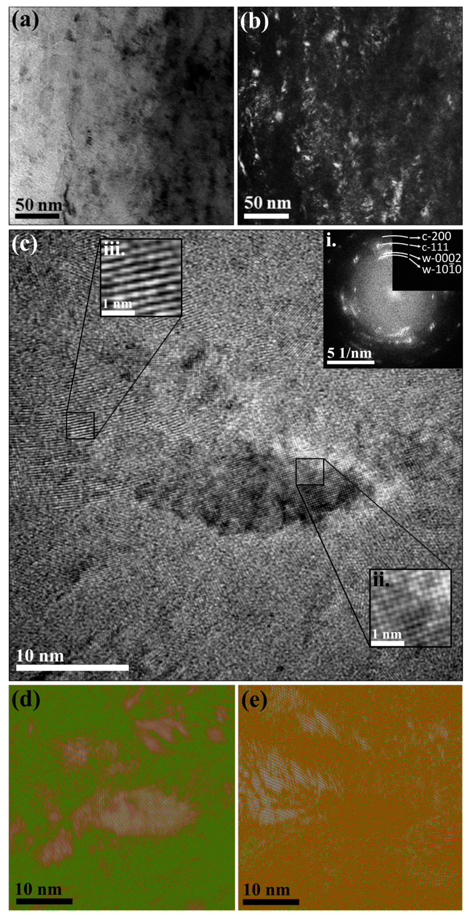
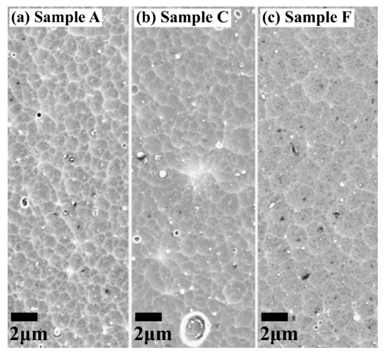
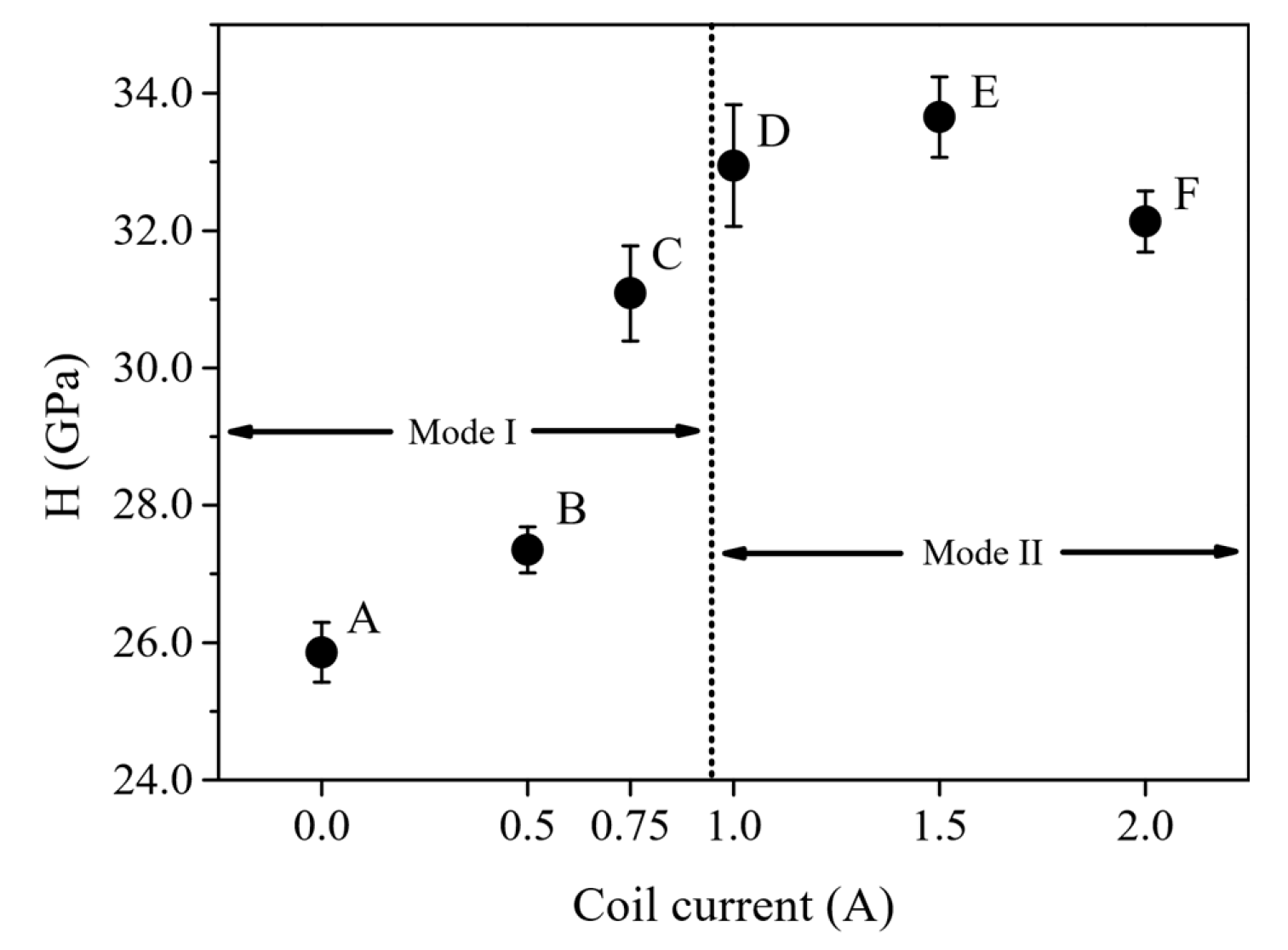
The depositions were performed using an industrial arc deposition system (Oerlikon Balzers Innova, Balzers, Liechtenstein) equipped with six 160-mm circular arc sources mounted on the chamber walls such that a homogeneous coating thickness was provided over the sample fixture. In the present study, three sources 120° apart and equipped with Ti0.33Al0.67 cathodes were used (Figure 1). The chamber walls act as an anode, while an additional annular anode was placed around each cathode. Two different types of substrates were used: cemented carbide WC-12 wt.% Co blank inserts (ISO SNUN120408) and 10 cm × 10 cm iron foils (Goodfellow Cambridge Ltd FE000400, Huntingdon, UK). The substrates were first cleaned in an ultrasonic alkaline bath and then mounted along a vertical line on a single rotating fixture. Next, the fixture was inserted into the deposition system with a resulting substrate-to-cathode distance of 15 cm and evacuated to a base pressure of less than 5 × 10⁻⁴ Pa. Before starting the deposition, the substrates were further cleaned by etching with Ar ions. All the depositions were performed in 3.5-Pa reactive N2 atmosphere while applying a constant negative bias voltage of 60 V, a fixed arc current of 180 A, and a fixture rotation of 3 rpm for a constant deposition time of 125 min.
A magnetic system consisted of a combination of three permanent magnet rings, and an additional electromagnetic coil (Figure 1) was used to steer cathode spots. It was placed behind each of the arc sources and outside the grounded vacuum chamber. The strength of the generated magnetic field was varied by applying DC coil currents between 0–2 A, resulting in different magnetic field configurations. The magnetic field at the cathode surface was simulated by using a finite element software (FEMM version 4.2). The validity of the simulated magnetic flux density was confirmed by measuring the magnetic flux density along a straight line from the cathode center to the periphery with a gaussmeter (Lake Shore 421, Westerville, OH, USA) using a flat Hall probe.
Plasma characterization was performed by optical emission spectrometry (OES) using a Mechelle 900 spectrometer (Oxford Instruments, Abingdon, UK) connected to a SensiCam 12Bit CCD camera (PCO, Kelheim, Germany), having a spectral range between 330–1200 nm and a resolving power (λ/Δλ) of approximately 900 [29]. The OES signal was acquired from the outside of the vacuum chamber through a glass viewport using a collimator directed toward the cathode surface. Then, the light was guided to the spectrometer by an optical fiber. Acquisitions were performed by summing 40 frames, each with an exposure time of 100 ms. The following lines were identified and analyzed: neutral Ti (Ti I, 498.17 nm) [30], neutral Al (Al I, 394.40 nm) [31], singly ionized Ti (Ti II, 368.52 nm) [32], singly ionized Al (Al II, 466.30 nm) [31], doubly ionized Ti (Ti III, 519.34 nm) [33], the first (B3Πg → A3Σ+u) and second (C3Πu → B3Πg) positive system of neutral molecular nitrogen (N2) [34], and the first negative system (B2Σ+u → X2Σ+g) from singly ionized molecular nitrogen (N2+) [34].
The arc spot motion on the cathode surface was recorded with a Phantom V90 high-speed camera (Wayne, NJ, USA) using a frame rate of 130 µs, through a viewport positioned at an angle of 45° to the surface normal of the cathode. The plasma plumes were also recorded at an angle close to 90° to the surface normal of the cathode using a Nikon D5000 camera (Nikon, Tokyo, Japan) with an exposure time of 4 ms.
The coating’s surface morphology was determined by scanning electron microscopy (SEM) using a Leo 1550 Gemini instrument (Zeiss, Oberkochen, Germany) with a working distance of 5 mm and an acceleration voltage of 5 kV. The coating’s composition was determined by using an Oxford X-Max 80 mm2 energy-dispersive X-ray spectroscopy (EDS) probe attached to the SEM with a working distance of 8.5 mm and an acceleration voltage of 20 kV. A cobalt reference sample and a set of (Ti,Al)N coatings with known compositions (determined by energy elastic recoil detection analysis) were used for energy and sensitivity calibrations. The metal-to-nitrogen ratio was assumed to be one, which has proven to be valid for arc-deposited (Ti,Al)N coatings grown at these N2 pressures [19]. Minor composition deviations between coatings A to F are within the EDX resolution limit (5 at.%) [35].
The microstructure of the coatings was investigated by transmission electron microscopy (TEM) using a FEI Tecnai G 2 TF 20 UT instrument (Hillsboro, OR, USA) operated at an acceleration voltage of 200 kV. Cross-sectional TEM samples were prepared by means of mechanical grinding and the polishing of thin slabs of the sample mounted in a Ti grid followed by Ar ion beam milling until electron transparency is achieved by using a Gatan Precision Ion Polishing System (Pleasanton, CA, USA). Plan view samples were sectioned with a Gatan Ultrasonic Disc Cutter model 601 and then mechanically polished and Ar ion milled to electron transparency. Recorded TEM micrographs were analyzed with the Gatan DigitalMicrographTM software (version 3.4).
A PANalytical X’Pert PRO X-ray diffractometer (Almelo, The Netherlands) operated in Bragg-Brentano θ/2θ configuration and using Cu-Kα radiation (0.154 nm) was used for phase determination of (Ti,Al)N powder samples. The powder samples were obtained by dissolving the iron foil substrates in concentrated (37%) hydrochloric acid. The coating flakes were recovered from the solution, washed with deionized water, and manually ground to a fine powder using mortar and pestle.
The residual stress of (Ti,Al)N coatings on WC–Co substrates was evaluated using the sin2 ψ method [36] of the 200 diffraction peak. An elastic modulus of 427 GPa and Poisson’s ratio of 0.25 [37] were used for the stress analysis.
The hardness was determined by an UMIS 2000 nanoindenter (Fischer-Cripps, Sydney, Australia) using a Berkovich diamond tip. Indents were performed on polished tapered cross-sections (~8° tapering angle) using a maximum load of 50 mN. The hardness was extracted from the load–displacement curve using the Oliver-Pharr method [38]. The reported hardness is an average from 30 indentations made on each sample.

3. Results

The investigated coatings, labeled A to F based on their respective applied coil currents, are shown in Table 1, together with their compressive residual stress and thickness. A change of the coil current from 0 (coating A) to 2 A (coating F) results in a reduction of the coating thickness from 15.2 (coating A) to 7.5 µm (coating F). The compressive residual stress decreases with increasing coil current from about ∔4.6 GPa for the sample grown with no coil current (coating A) to −3.4 and −3.6 GPa for coatings grown with a coil current of 1.5 and 2.0 A (coatings E and F), respectively. No difference in the chemical composition was observed between the investigated coatings.
Figure 2 shows the simulated magnetic flux density for the coil currents of 0 (Figure 2a) and 2 A (Figure 2b), and the trace of the cathode spots for 0 (Figure 2c) and 2 A (Figure 2d) captured by a high-speed camera and obtained by overlaying multiple frames that correspond to one revolution of the spot on the cathode surface. For 0 A (Figure 2a), the magnetic field lines are parallel to the cathode surface approximately a quarter of the way from the cathode center to its edge, and the magnetic flux density at this region is considerably low. For 2 A (Figure 2b), the magnetic field lines are parallel to the cathode surface closer to its edge, and the magnetic flux density is higher than for 0 A. In the 2 A coil current case, the magnetic field lines close to the cathode edge appear to be guided toward the annular anode. The cathode spot resides predominantly approximately 35 mm from the cathode center (Figure 2c) when no coil current (0 A) is applied and multiple spots are visible in each frame. The latter indicates cathode spot splitting. For a coil current of 2 A (Figure 2d), the cathode spot appears to be confined closer to the cathode periphery (approximately 75 mm from the center). The information recorded by the high-speed camera (Figure 2c,d) can be used to estimate the mean velocity (v) of the cathode spot by the relation:
v = (2πr)/(Number of frames × exposure time)
For the coil current of 0 A (r = 35 mm, number of frames for one complete revolution of the spot over the cathode was 45 frames), the velocity of the cathode spot is approximately 37 m/s, while for the coil current of 2 A (r = 75 mm, number of frames for one complete revolution of the spot over the cathode = 71 frames), it is approximately 52 m/s.
Figure 3 depicts cross-sectional images of the plasma plume, for a coil current of 0 A is shown in Figure 3a, and for 2 A, it is shown in Figure 3b. A change in coil current from 0 to 2 A results in a reduction of the plasma density. The side view of the plasma plume emanating from the cathode is schematically portrayed for 0 (Figure 3c) and 2 A (Figure 3d) coil currents. The schemes are intended to show the spread of the plasma in a radial fashion toward the cathode edges that takes place as the cathode spots are steered to the cathode surface periphery (Figure 3c,d) with increasing coil current. The changes in plasma density when changing the coil current is represented by the pseudocolor in Figure 3c,d.
Figure 4 shows the deposition rate, burning voltage, and bias current at the substrate holder as functions of the electromagnet coil current of the arc source. The included charge-to-mass ratio (Q/M) is determined as the ratio between the bias current and the deposition rate [28]. The charge-to-mass ratio (Q/M) is related to the ionization degree of the plasma and represents the ionized species involved in the deposition process. In order to compare the Q/M ratio between coatings A–F, their densities need to be similar. The Q/M ratio decreases between coatings A (0 A coil current) and D (1 A coil current). Between 1 and 2 A, the Q/M ratio remains almost constant.
An increase of about 2 V in burning voltage from 0 to 2 A is observed. Growth Modes I and II, as indicated in Figure 4, are identified by comparing grain size and phase compositions (i.e., the presence of B4 in addition to the B1 phase) of coatings A–F.
Figure 5a shows OES results of the plasma for the wavelengths 332–401 and 565–780 nm at different coil currents (0 to 2 A). The emission lines observed are from neutral and singly ionized titanium (Ti I, Ti II), neutral aluminum (Al I), the first (B3Πg → A3Σ+u) and second (C3Πu → B3Πg) positive systems of neutral molecular nitrogen (N2), and the first negative system (B2Σ+u → X2Σ+g) from singly ionized molecular nitrogen (N2+). In addition, singly ionized Al (Al II, 466.30 nm) [31], doubly ionized Ti (Ti III, 467.33 and 519.34 nm) [33], and doubly ionized Al (Al III, 447.99 and 451.25 nm) [39] were also observed. The line intensities of all the observed species decrease with increasing coil current. Such a decrease is particularly evident for the molecular nitrogen bands shown in Figure 5b. It is well known that cathodic arc plasma contains multiply charged species [40]. Al IV, Ti IV, and Ti V lines that exist in the 10 to 300 nm wavelength range [41,42,43,44] are not observed here due to the absorption of wavelengths below about 330 nm by the viewport glass of the chamber. Additionally, Ti IV lines between 748–770 nm are overlapped by N2 lines and have weak intensities.
Figure 6 shows the decrease in optical emission intensity of all plasma species, as the coil current is increased. This decrease indicates that significantly less excitation takes place in Mode II in comparison with Mode I, which is in line with the photographs of the plasma plume (Figure 3a,b).
Figure 7 shows (a) powder X-ray diffractograms and (b) a magnified portion of the same diffractograms for coatings B and C. Coatings A, B, and C (Mode I) exhibit a dual B1 (c-(TiAl)N) and B4 (w-(TiAl)N) phase structure. The intensities of the B4 peaks (marked with squares) decrease with increasing the coil current. Coatings D, E, and F (Mode II) exhibit a single phase B1 structure, and the diffractograms from coatings E and F (1.5 and 2 A) are close to identical. No B4 phase was within the detection limit for the X-ray diffraction technique that was found in these samples. The transition from a dual to a single-phase coating structure occurs for a coil current between 0.75–1 A.
Cross-sectional and plan view TEM micrographs including selective area electron diffraction (SAED) patterns of coatings A, C, and F are shown in Figure 8. All coatings display diffuse contrast, which is typical for arc-deposited coatings, caused by the high number of point defects (vacancies and interstitials) [45]. The micrograph of coating A (Figure 8(aii)) shows nanocrystalline grains slightly elongated in the growth direction. The SAED inset confirms the presence of both B1 and B4 phases. The corresponding plan-view micrograph of coating A shows domains with a globular shape (Figure 8(ai)). Coating C displays a more elongated (columnar shape) microstructure with coarser domains compared to coating A (Figure 8(bii)). Similar to the XRD results, the intensity of the SAED from B4 decreases when increasing the coil current, which is consistent with a decrease in the amount of the B4 phase. The plan view of coating C (Figure 8(bi)) reveals a coarser globular structure compared to coating A (Figure 8(ai)). Coating F exhibits a dense microstructure consisting of columns in the growth direction, and the SAED shows a single phase (B1) (Figure 8(cii)). The microstructure of coating F (Figure 8c) is considerably coarser than coatings A (Figure 8a) and C (Figure 8b).
The coatings are all dense without any apparent voids (Figure 8). The B4 phase, with approximately 17% lower density than the B1 phase, only exists in small amounts (<10 vol.%) in coatings A, B, and C (Figure 7). Hence, the assumption of similar densities of all the coatings for measuring the Q/M ratio (see Figure 4) is valid. The Q/M ratio reduction by ~12% as the coil current increases from 0 to 2 A is significantly larger than the contribution from the differences in phase composition.
Figure 9a shows bright-field and Figure 9b shows dark-field TEM micrographs of coating A. The dark-field image was obtained mainly from the B4 phase showing small crystallites. A high-resolution TEM (Figure 9c) with a fast Fourier transform (FFT) inset (9(ci)) was used to further characterize the B4 phase in the coating. The FFT pattern could be indexed with both B1 and B4 phases. Lattice fringes of the B1 and B4 phases are shown as insets 9(cii) and 9(ciii), respectively. Figure 9d shows the inverse-FFT only selecting the c-111 and c-200 rings. Figure 9e shows the inverse-FFT by selecting w-10 1 ¯ 0 and w-0002 rings.
Figure 10 shows SEM micrographs depicting the surface morphology of coatings A (a), C (b), and F (c). The three coatings exhibit similar amount of droplets and densified structures, which resulted from the ion flux bombardment. The surface of coating F (c) is smoother compared to coatings A (a) and C (b).
Figure 11 shows the as-deposited coating hardness with increasing coil current from 0 (coating A) to 2 A (coating F). The most significant hardness increase takes place between coatings B (0.5 A) and C (0.75 A). The highest hardness values are observed within Mode II.

4. Discussion

The deposition flux emanating from a cathodic arc source is known to be highly ionized [46] with a total arc current containing approximately 90% electrons and 10% ions [47,48]. Since electrons have the lowest inertia among the charged species in the plasma, they are most easily influenced by the magnetic field. In a magnetically steered arc process, the electric field (E) due to the cathode fall and the arc steering magnetic field (B) shown in Figure 2 create an E×B drift current. The E × B drift current has its highest density in regions where the vector product (E × B) is maximum, or in other words, where the magnetic field is parallel to the cathode surface. This leads to an anisotropy in the electric field at the cathode surface [49]. The field emission of electrons is enhanced at the regions where the magnetic field is parallel to the cathode surface, which increases the probability of cathode spot ignition at such regions [50]. This phenomenon is sometimes referred to as the acute angle rule [51].
In Mode I operation of the present work, the applied magnetic field is parallel to the cathode surface at a position midway from center to its periphery (Figure 2a). As an effect, this will cause the cathode spots to predominantly ignite midway from cathode center to its edge (Figure 2c). The splitting of the cathode spot in Mode I (Figure 2c) indicates that the intrinsic magnetic field generated by the arc in the cathode spot region is stronger than the applied extrinsic arc guiding magnetic field [52].
However, in Mode II operation, the higher coil current produces a magnetic field that becomes parallel to the cathode surface closer to the cathode periphery (Figure 2b) and, as a result, the cathodes spots are ignited closer to the edge (Figure 2d). Since the magnetic field at such location is about twice as strong as in Mode I (Figure 2a,b), the cathode spot appears to be confined, and thus no cathode spot splitting is observed. The combination of cathode spots residing closer to the annular anode, a stronger magnetic field, and the magnetic field lines curving toward the annular anode in Mode II guides electrons emanating from the cathode spot more effectively to the annular anode [53] (Figure 2). Due to electron-ion coupling [54,55], the ions will also follow the trajectory of the electrons, and thus the plasma plume expands sideways from the cathode in Mode II compared to Mode I (Figure 3). Consequently, a decreased plasma density in the direction toward the substrates is expected, and less of the evaporated flux reaches the substrate position, which explains the lower deposition rate observed in Mode II.
The increase in the cathode spot velocity in Mode II is an indirect indication of a lower plasma density. The lower plasma density in Mode II increases the process impedance, which causes the cathode spot to quench more quickly; in other words, it shortens the dwell time of each cathode spot, which ultimately increases the apparent cathode spot velocity. The burning voltage of the cathode is an indication of the process impedance [56], while the plasma density has an inverse correlation with the process impedance. The lean plasma in Mode II is expected to increase the process impedance, and hence the burning voltage. The observed increase in burning voltage in Mode II (Figure 4) corroborates the deduction that the plasma density in Mode II decreases.
Electron-impact ionization is the predominant source of gas phase ionization [57], and N2 ionization is known to occur at a significant distance from the cathode [58]. In Mode II, the loss of electrons to the annular anode causes a reduction in the probability of electron-impact ionization events. It suggests a lower N2 ionization in Mode II, which is seen as a 12% reduction of the Q/M values (Figure 4).
The coatings deposited in Mode I and Mode II show similar composition, which suggests that the plasma composition is similar for both modes, and the main difference is the ionization of the plasma species, as represented by Q/M (Figure 4). Under the influence of bias voltage, the ionization degree of the plasma (Q/M) is proportional to the energy delivered at the growth front of the coatings per depositing species. Since Q/M is 12% higher in Mode I compared to Mode II, the energy delivered per species is higher in Mode I than in Mode II, and as discussed above, this difference can be mainly attributed to nitrogen ionization. For the composition of Ti0.33Al0.67N, the enthalpy of formation of the B4 phase is merely 0.02 eV/atom higher than that of the B1 phase, since the Ti/(Ti + Al) ratio of 0.67 is very close to the crossover composition of 0.71 [59]. The higher energy delivered at the coating growth front in Mode I and the small difference in the enthalpies of formation between B1 and B4 lead to a situation where it is possible to nucleate the B4 phase in parallel to the B1 phase (Figure 5, Figure 6 and Figure 7). Such parallel nucleation of the B1 and B4 phases leads to an increased nucleation rate, while the growth of the nuclei is suppressed by additional nuclei forming. This results in fine-grained microstructures of coatings deposited in Mode I, as can be seen in Figure 8 and Figure 9. The decrease in the Q/M ratio (Figure 4) as the coil current increases (in Mode I) causes a decrease in the amount of the B4 phase (Figure 7) and an increase of the grain size (Figure 8), which is consistent with a lower nucleation rate (lower probability of B4 formation) at the coating growth front. Single-phase B1 coatings are formed (Mode II) when the coil current is high enough to sufficiently reduce the deposition rate and energy delivered to the growth front to inhibit B4 nucleation. The observed detrimental effect of the B4 phase on the hardness (Figure 11) of (Ti,Al)N coatings is well established [60].

5. Conclusions

The growth of high Al content (Ti,Al)N coatings was carried out with a modified cathodic arc deposition setup with a magnetic assembly consisted of permanent magnets and an electromagnetic coil located on the backside of the arc source. The additional magnetic field, applied through the electromagnetic coil, ensued:
  • the cathode spots to reside at the periphery of the cathode;
  • the increase in cathode spot velocity;
  • a decrease in plasma density;
  • a decrease in the deposition rate, and
  • a decrease of ionization of the plasma species.
Consequently, two distinct growth modes were identified. In Mode I, with no additional magnetic field, fine-grained dual-phase (B1 and B4) coatings were grown. The presence of the B4 phase was detrimental to the coating’s hardness, as observed in Mode I. In Mode II, with an additional magnetic field, a lower energy flux was delivered to the coating’s growth front, which reduced surface diffusion and suppressed the formation of the B4 phase. As a result, the growth of coarse columnar-grained single phase (B1) coatings took place in Mode II.
It is concluded that the additional magnetic field generated by the electromagnetic coil offers an effective means to control the microstructure of (Ti0.36Al0.64)N coatings.

Author Contributions

Conceptualization, methodology, and validation: A.B.B.C., B.S., M.J.-J. and M.O.; investigation: A.B.B.C., B.S. and T.-W.H.; writing—original draft preparation: A.B.B.C. and B.S.; writing—review and editing: M.J.-J., J.M.A., G.H., L.J.S.J. and M.O.; supervision: M.J.-J., F.M. and M.O.

Funding

This research was funded by the Swedish Research Council, grant number 621-2012-4401; the Swedish government strategic research area grant AFM-SFO MatLiU 2009-00971, and the VINNOVA FunMat-II, grant number 2016-05156.

Acknowledgments

A.B.B.C. acknowledges the support from the European Union’s Erasmus Mundus doctoral program in Materials Science and Engineering (DocMASE) and the Roberto Rocca Doctorate Fellowship. We thank M. Ahlgrén, M. Saraiva and K. Edlund for the help with coating depositions, L. Karlsson and Gied Rutten for the OES acquisitions, and N. Ghafoor for the TEM operation.

Conflicts of Interest

The authors declare no conflict of interest. The funders had no role in the design of the study; in the collection, analyses, or interpretation of data; in the writing of the manuscript, or in the decision to publish the results.

References

  1. Munz, W.D. Titanium aluminum nitride films—A new alternative to tin coatings. J. Vac. Sci. Technol. A 1986, 4, 2717–2725. [Google Scholar] [CrossRef]
  2. Knutsson, A.; Ullbrand, J.; Rogstrom, L.; Norrby, N.; Johnson, J.S.; Hultman, L.; Almer, J.; Joesaar, M.P.J.; Jansson, B.; Oden, M. Microstructure evolution during the isostructural decomposition of TiAlN-A combined in-situ small angle X-ray scattering and phase field study. J. Appl. Phys. 2013, 113, 213518. [Google Scholar] [CrossRef]
  3. Bartosik, M.; Rumeau, C.; Hahn, R.; Zhang, Z.L.; Mayrhofer, P.H. Fracture toughness and structural evolution in the TiAlN system upon annealing. Sci. Rep. 2017, 7, 16476. [Google Scholar] [CrossRef] [PubMed]
  4. Horling, A.; Hultman, L.; Oden, M.; Sjolen, J.; Karlsson, L. Mechanical properties and machining performance of Ti1−xAlxN-coated cutting tools. Surf. Coat. Technol. 2005, 191, 384–392. [Google Scholar] [CrossRef]
  5. Holleck, H. Metastable coatings—Prediction of composition and structure. Surf. Coat. Technol. 1988, 36, 151–159. [Google Scholar] [CrossRef]
  6. Greczynski, G.; Mraz, S.; Hans, M.; Lu, J.; Hultman, L.; Schneider, J.M. Control over the phase formation in metastable transition metal nitride thin films by tuning the Al+ subplantation depth. Coatings 2019, 9, 17. [Google Scholar] [CrossRef]
  7. Shulumba, N.; Hellman, O.; Raza, Z.; Alling, B.; Barrirero, J.; Mucklich, F.; Abrikosov, I.A.; Oden, M. Lattice vibrations change the solid solubility of an alloy at high temperatures. Phys. Rev. Lett. 2016, 117, 205502. [Google Scholar] [CrossRef]
  8. Horling, A.; Hultman, L.; Oden, M.; Sjolen, J.; Karlsson, L. Thermal stability of arc evaporated high aluminum-conteht Ti1−xAlxN thin films. J. Vac. Sci. Technol. A 2002, 20, 1815–1823. [Google Scholar] [CrossRef]
  9. Rogstrom, L.; Ullbrand, J.; Almer, J.; Hultman, L.; Jansson, B.; Oden, M. Strain evolution during spinodal decomposition of TiAlN thin films. Thin Solid Film 2012, 520, 5542–5549. [Google Scholar] [CrossRef] [Green Version]
  10. Calamba, K.M.; Pierson, J.F.; Bruyere, S.; Febvrier, A.L.; Eklund, P.; Barrirero, J.; Mucklich, F.; Boyd, R.; Joesaar, M.P.J.; Oden, M. Dislocation structure and microstrain evolution during spinodal decomposition of reactive magnetron sputtered heteroepixatial c-(Ti-0.37,Al-0.63)N/c-TiN films grown on MgO(001) and (111) substrates. J. Appl. Phys. 2019, 125, 105301. [Google Scholar] [CrossRef]
  11. Tasnadi, F.; Abrikosov, I.A.; Rogstrom, L.; Almer, J.; Johansson, M.P.; Oden, M. Significant elastic anisotropy in Ti1−xAlxN alloys. Appl. Phys. Lett. 2010, 97, 231902. [Google Scholar] [CrossRef]
  12. Abrikosov, I.A.; Knutsson, A.; Alling, B.; Tasnadi, F.; Lind, H.; Hultman, L.; Oden, M. Phase stability and elasticity of TiAlN. Materials (Basel) 2011, 4, 1599–1618. [Google Scholar] [CrossRef] [PubMed]
  13. Wang, S.Q.; Chen, K.H.; Chen, L.; Zhu, C.J.; Li, P.; Du, Y. Effect of Al and Si additions on microstructure and mechanical properties of TiN coatings. J. Cent. South Univ. Technol. 2011, 18, 310–313. [Google Scholar] [CrossRef]
  14. Kim, B.J.; Kim, Y.C.; Nah, J.W.; Lee, J.J. High temperature oxidation of Ti1−xAlxN coatings made by plasma enhanced chemical vapor deposition. J. Vac. Sci. Technol. A 1999, 17, 133–137. [Google Scholar] [CrossRef]
  15. Koller, C.M.; Hollerweger, R.; Sabitzer, C.; Rachbauer, R.; Kolozsvari, S.; Paulitsch, J.; Mayrhofer, P.H. Thermal stability and oxidation resistance of arc evaporated TiAlN, TaAlN, TiAlTaN, and TiAlN/TaAlN coatings. Surf. Coat. Technol. 2014, 259, 599–607. [Google Scholar] [CrossRef]
  16. Greczynski, G.; Hultman, L.; Odén, M. X-ray photoelectron spectroscopy studies of Ti1−xAlxN (0 ≤ x ≤ 0.83) high-temperature oxidation: The crucial role of Al concentration. Surf. Coat. Technol. 2019, 374, 923–934. [Google Scholar] [CrossRef]
  17. Norrby, N.; Rogstrom, L.; Johansson-Joesaar, M.P.; Schell, N.; Oden, M. In situ X-ray scattering study of the cubic to hexagonal transformation of A1N in Ti1−xAlxN. Acta Mater. 2014, 73, 205–214. [Google Scholar] [CrossRef]
  18. Joesaar, M.P.J.; Norrby, N.; Ullbrand, J.; M’Saoubi, R.; Oden, M. Anisotropy effects on microstructure and properties in decomposed arc evaporated Ti1−xAlxN coatings during metal cutting. Surf. Coat. Technol. 2013, 235, 181–185. [Google Scholar] [CrossRef]
  19. Baben, M.T.; Hans, M.; Primetzhofer, D.; Evertz, S.; Ruess, H.; Schneider, J.M. Unprecedented thermal stability of inherently metastable titanium aluminum nitride by point defect engineering. Mater. Res. Lett. 2017, 5, 158–169. [Google Scholar] [CrossRef]
  20. Norrby, N.; Lind, H.; Parakhonskiy, G.; Johansson, M.P.; Tasnadi, F.; Dubrovinsky, L.S.; Dubrovinskaia, N.; Abrikosov, I.A.; Oden, M. High pressure and high temperature stabilization of cubic AlN in Ti0.60Al0.40N. J. Appl. Phys. 2013, 113, 053515. [Google Scholar] [CrossRef]
  21. Shulumba, N.; Raza, Z.; Hellman, O.; Janzen, E.; Abrikosov, I.A.; Oden, M. Impact of anharmonic effects on the phase stability, thermal transport, and electronic properties of AlN. Phys. Rev. B 2016, 94, 104305. [Google Scholar] [CrossRef] [Green Version]
  22. Alling, B.; Oden, M.; Hultman, L.; Abrikosov, I.A. Pressure enhancement of the isostructural cubic decomposition in Ti1−xAlxN. Appl. Phys. Lett. 2009, 95, 181906. [Google Scholar] [CrossRef]
  23. Knutsson, A.; Johansson, M.P.; Karlsson, L.; Oden, M. Thermally enhanced mechanical properties of arc evaporated Ti(0.34)Al(0.66)N/TiN multilayer coatings. J. Appl. Phys. 2010, 108, 044312. [Google Scholar] [CrossRef]
  24. Forsen, R.; Johansson, M.; Oden, M.; Ghafoor, N. Decomposition and phase transformation in TiCrAlN thin coatings. J. Vac. Sci. Technol. A 2012, 30, 061506. [Google Scholar] [CrossRef]
  25. Schramm, I.C.; Joesaar, M.P.J.; Jensen, J.; Mucklich, F.; Oden, M. Impact of nitrogen vacancies on the high temperature behavior of (Ti1−xAlx)Ny alloys. Acta Mater. 2016, 119, 218–228. [Google Scholar] [CrossRef]
  26. Greczynski, G.; Lu, J.; Johansson, M.; Jensen, J.; Petrov, I.; Greene, J.E.; Hultman, L. Selection of metal ion irradiation for controlling Ti1−xAlxN alloy growth via hybrid HIPIMS/magnetron co-sputtering. Vacuum 2012, 86, 1036–1040. [Google Scholar] [CrossRef]
  27. Mayrhofer, P.H.; Geier, M.; Löcker, C.; Chen, L. Influence of deposition conditions on texture development and mechanical properties of TiN coatings. Int. J. Mater. Res. 2009, 100, 1052–1058. [Google Scholar] [CrossRef] [Green Version]
  28. Andersson, J.M.; Vetter, J.; Müller, J.; Sjölén, J. Structural effects of energy input during growth of Ti1−xAlxN (0.55 ≤ x ≤ 0.66) coatings by cathodic arc evaporation. Surf. Coat. Technol. 2014, 240, 211–220. [Google Scholar] [CrossRef]
  29. Sarzynski, A.; Skrzeczanowski, W.; Marczak, J. Possibility of the Mechelle 900 spectrometer applications for artwork and technology research. Proc. SPIE 2007, 6598, 65980U. [Google Scholar] [CrossRef]
  30. Forsberg, P. The spectrum and term system of neutral titanium, Ti-I. Phys. Scr. 1991, 44, 446–476. [Google Scholar] [CrossRef]
  31. Kaufman, V.; Martin, W.C. Wavelengths and energy-level classifications for the spectra of aluminum (Al-I through Al-Xiii). J. Phys. Chem. Ref. Data 1991, 20, 775–858. [Google Scholar] [CrossRef]
  32. Sugar, J.; Corliss, C. Atomic-energy levels of the iron-period elements—Potassium through nickel. J. Phys. Chem. Ref. Data 1985, 17, 680. [Google Scholar]
  33. Edlen, B.; Swensson, J.W. Spectrum of doubly ionized titanium, Ti III. Phys. Scr. 1975, 12, 21–32. [Google Scholar] [CrossRef]
  34. Lofthus, A.; Krupenie, P.H. Spectrum of molecular nitrogen. J. Phys. Chem. Ref. Data 1977, 6, 113–307. [Google Scholar] [CrossRef]
  35. Waldo, R.A.; Militello, M.C.; Gaarenstroom, S.W. Quantitative thin-film analysis with an energy-dispersive X-ray detector. Surf. Interface Anal. 1993, 20, 111–114. [Google Scholar] [CrossRef]
  36. Cullity, B.D.; Stock, S.R. Elements of X-ray Diffraction, 2nd ed.; Prentice Hall: Upper Saddle River, NJ, USA, 2001. [Google Scholar]
  37. Maxwell, A.S.; Owen-Jones, S.; Jennett, N.M. Measurement of Young’s modulus and Poisson’s ratio of thin coatings using impact excitation and depth-sensing indentation. Rev. Sci. Instrum. 2004, 75, 970–975. [Google Scholar] [CrossRef]
  38. Oliver, W.C.; Pharr, G.M. An improved technique for determining hardness and elastic-modulus using load and displacement sensing indentation experiments. J. Mater. Res. 1992, 7, 1564–1583. [Google Scholar] [CrossRef]
  39. Isberg, B. The spectrum of doubly ionized aluminium, Al III. Ark. Fys. (Stockh.) 1968, 35, 551–562. [Google Scholar]
  40. Hashmi, S.; Batalha, G.F.; Van Tyne, C.J.; Yilbas, B.S. Comprehensive Materials Processing; Elsevier: Amsterdam, The Netherlands, 2014; Chapter 14; Volume 13, p. 315. [Google Scholar]
  41. Artru, M.-C.; Kaufman, V. Extension of the analysis of triply ionized aluminum (Al IV). J. Opt. Soc. Am. 1975, 65, 594–599. [Google Scholar] [CrossRef]
  42. Svensson, L.A. The spectrum of four-times-ionized titanium, Ti V. Phys. Scr. 1976, 13, 235–239. [Google Scholar] [CrossRef]
  43. Artru, M.-C.; Brillet, W.-Ü.L. Analysis of the spectrum of quadruply ionized aluminum (Al V). J. Opt. Soc. Am. 1974, 64, 1063–1071. [Google Scholar] [CrossRef]
  44. Swensson, J.W.; Edlén, B. The spectrum of three times ionized titanium, Ti IV. Phys. Scr. 1974, 9, 335–337. [Google Scholar] [CrossRef]
  45. Oden, M.; Almer, J.; Hakansson, G. The effects of bias voltage and annealing on the microstructure and residual stress of arc-evaporated Cr–N coatings. Surf. Coat. Technol. 1999, 120, 272–276. [Google Scholar] [CrossRef]
  46. Bilek, M.M.M.; Martin, P.J.; McKenzie, D.R. Influence of gas pressure and cathode composition on ion energy distributions in filtered cathodic vacuum arcs. J. Appl. Phys. 1998, 83, 2965–2970. [Google Scholar] [CrossRef] [Green Version]
  47. Kimblin, C.W. Erosion and ionization in the cathode spot regions of vacuum arcs. J. Appl. Phys. 1973, 44, 3074–3081. [Google Scholar] [CrossRef]
  48. Daalder, J.E. Components of cathode erosion in vacuum arcs. J. Phys. D Appl. Phys. 1976, 9, 2379. [Google Scholar] [CrossRef]
  49. Anders, A. Discharge physics of high power impulse magnetron sputtering. Surf. Coat. Technol. 2011, 205, S1–S9. [Google Scholar] [CrossRef] [Green Version]
  50. Swift, P.D. Macroparticles in films deposited by steered cathodic arc. J. Phys. D Appl. Phys. 1996, 29, 2025–2031. [Google Scholar] [CrossRef]
  51. Anders, A. Cathodic Arcs: From Fractal Spots to Energetic Condensation; Springer: New York, NY, USA, 2008; p. 233. [Google Scholar]
  52. Beilis, I.I. Mechanism of cathode spot splitting in vacuum arcs in an oblique magnetic field. Phys. Plasmas 2015, 22, 103510. [Google Scholar] [CrossRef]
  53. Kurapov, D.; Krassnitzer, S. Aluminum Titanium Nitride Coating with Adapted Morphology for Enhanced Wear Resistance in Machining Operations and Method Thereof. U.S. Patent 9,447,488 B2, 4 April 2013. [Google Scholar]
  54. Sanders, D.M.; Anders, A. Review of cathodic arc deposition technology at the start of the new millennium. Surf. Coat. Technol. 2000, 133, 78–90. [Google Scholar] [CrossRef]
  55. Rosen, J.; Anders, A.; Mraz, S.; Schneider, J.M. Charge-state-resolved ion energy distributions of aluminum vacuum arcs in the absence and presence of a magnetic field. J. Appl. Phys. 2005, 97, 103306. [Google Scholar] [CrossRef]
  56. Anders, A.; Yushkov, G.Y. Ion flux from vacuum arc cathode spots in the absence and presence of a magnetic field. J. Appl. Phys. 2002, 91, 4824–4832. [Google Scholar] [CrossRef] [Green Version]
  57. Lieberman, M.A.; Lichtenberg, A.J. Principles of Plasma Discharges and Materials Processing, 2nd ed.; Wiley-Interscience: Hoboken, NJ, USA, 2005; Chapter 3; p. 43. [Google Scholar]
  58. Franz, R.; Polcik, P.; Anders, A. Element- and charge-state-resolved ion energies in the cathodic arc plasma from composite AlCr cathodes in argon, nitrogen and oxygen atmospheres. Surf. Coat. Technol. 2015, 272, 309–321. [Google Scholar] [CrossRef] [PubMed] [Green Version]
  59. Holec, D.; Rovere, F.; Mayrhofer, P.H.; Barna, P.B. Pressure-dependent stability of cubic and wurtzite phases within the TiN-AlN and CrN-AlN systems. Scr. Mater. 2010, 62, 349–352. [Google Scholar] [CrossRef]
  60. Bartosik, M.; Daniel, R.; Zhang, Z.; Deluca, M.; Ecker, W.; Stefenelli, M.; Klaus, M.; Genzel, C.; Mitterer, C.; Keckes, J. Lateral gradients of phases, residual stress and hardness in a laser heated Ti0.52Al0.48N coating on hard metal. Surf. Coat. Technol. 2012, 206, 4502–4510. [Google Scholar] [CrossRef] [PubMed] [Green Version]
Figure 1. Top-view schematic representation (not to scale) of the deposition setup used.
Coatings 09 00660 g001
Figure 2. Schematic representation (not to scale) of the cathode, annular anode, and magnetic system (permanent magnet rings and electromagnetic coil) with simulated magnetic flux density for the coil currents of 0 (a) and 2 A (b), the strength of magnetic flux density is proportional to the greyscale color which can be read from (e). The approximate regions where the magnetic field lines are parallel to the cathode surface are indicated by arrows. Images of Ti0.33Al0.67 cathode surfaces during arc evaporation (180 A arc current, 3.5 Pa of N2) were recorded with a high-speed camera placed at 45° with respect to the surface normal and using an exposure time of 130 µs for each frame. In (c), the coil current is 0 A, and the image is the sum of 45 frames, and in (d), the coil current is 2 A coil, and the image is the sum of 71 frames.
Coatings 09 00660 g002
Figure 3. Side-view images (camera placed at 87° with respect to the surface normal) of the plasma plume emanating from the cathode are depicted for the cases of the 0 (a) and 2 A (b) coil currents. The pictures were acquired with an exposure of 4 ms. The cross-sections of the plasma plume are schematically drawn (not to scale) for the 0 (c) and 2 A (d) coil currents.
Coatings 09 00660 g003
Figure 4. Substrate bias current, deposition rate, charge-to-mass ratio (Q/M), and burning voltage as a function of the coil current applied during growth.
Coatings 09 00660 g004
Figure 5. Optical emission spectra recorded during deposition using different coil currents (0 to 2 A). (a) Lines for neutral and singly ionized Ti+ (Ti I and Ti II, respectively), neutral Al (Al I), the second positive system (C3Πu → B3Πg) of neutral molecular nitrogen (N2), and the first negative system (B2Σ+u → X2Σ+g) from singly ionized molecular nitrogen (N2+) are detected. (b) The first positive system (B3Πg → A3Σ+u) of neutral molecular nitrogen (N2) is depicted.
Coatings 09 00660 g005
Figure 6. Intensities of detected optical emission lines of neutral Ti (498.17 nm), singly ionized Ti+ (368.52 nm), doubly ionized Ti++ (519.34 nm), neutral Al (394.40 nm), singly ionized Al+ (466.30 nm), neutral N2 (337.72 nm), and singly ionized N2+ (391.62 nm), as a function of coil current.
Coatings 09 00660 g006
Figure 7. X-ray diffractograms showing (a) the phase content as a function coil current. (b) The presence of both B1 (cubic) and B4 (wurtzite) phases for coatings B and C.
Coatings 09 00660 g007
Figure 8. TEM micrographs of plan view (i), cross-section (ii) and selected area diffraction pattern (SAEDP) inset of as-deposited coatings A (a), C (b), and F (c), respectively. The SAEDPs of coatings A (a) and C (b) are indexed with mixed B1 and B4 phases, whereas the SAEDP of coating F (c) with a single phase B1 structure.
Coatings 09 00660 g008
Figure 9. Bright-field (a) and dark-field (b) transmission electron micrographs of coating A highlighting B4 domains. The high-resolution transmission electron micrograph of coating A is shown in (c). The insets depict the fast Fourier transform (FFT) (ci) of (c), and magnified lattices of the B1 (cii) and B4 (ciii) phases. The inverse FFT of (c) is shown based on the information of the cubic 111 and 200 rings in (d), while in (e), it is only based on the information of the wurtzite 10 1 ¯ 0 and 0002 rings.
Coatings 09 00660 g009
Figure 10. SEM micrographs showing the surface morphology of (a) coating A, (b) coating C, and (c) coating F.
Coatings 09 00660 g010
Figure 11. Hardness of coating as a function of coil current. Letters (A–F) indicate sample labeling (see Table 1).
Coatings 09 00660 g011
Table 1. Investigated coatings and their respective coil current, coating thickness, and residual stress.
Sample IDCoil Current (A)Coating Thickness (µm)Residual Stress (GPa)
A0.015 ± 0.4−4.6 ± 0.5
B0.512.4 ± 0.3−4.6 ± 0.5
C0.7510.9 ± 0.4−4.5 ± 0.4
D1.09.7 ± 0.4−4.4 ± 0.2
E1.59.1 ± 0.4−3.4 ± 0.2
F2.07.85 ± 0.3−3.6 ± 0.2

