Article

Influence of Bath Additives on the Thermal Stability of the Nanostructure and Hardness of Ni Films Processed by Electrodeposition

1
Department of Material Physics, ELTE Eötvös Loránd University, Pázmány Péter sétány 1/A, H-1117 Budapest, Hungary
2
Institute for Technical Physics and Materials Science, Centre for Energy Research, Hungarian Academy of Sciences, Konkoly-Thege M. út 29-33, H-1121 Budapest, Hungary
3
Wigner Research Centre for Physics, Hungarian Academy of Sciences, Konkoly-Thege út 29-33, H-1121 Budapest, Hungary
*
Author to whom correspondence should be addressed.
Coatings 2019, 9(10), 644; https://doi.org/10.3390/coatings9100644
Submission received: 29 August 2019 / Revised: 27 September 2019 / Accepted: 27 September 2019 / Published: 5 October 2019
(This article belongs to the Section Surface Characterization, Deposition and Modification)

Abstract

:
The effect of bath additives on the thermal stability of the microstructure and hardness of nanocrystalline Ni foils processed by electrodeposition was studied. Three samples with a thickness of 20 μm were prepared: one without any additive and two others with saccharin or trisodium citrate additives. Then, the specimens were heat-treated at different temperatures up to 1000 K. It was found that for the additive-free sample the recovery of the microstructure and the reduction of the hardness started only at temperatures higher than 500 K. At the same time, a decrease of the defect density and hardness was observed even at 400 K for the additive-containing films. This was explained by the higher defect density, which increased the thermodynamic driving force for recovery during annealing. At the highest applied temperature (1000 K), this larger thermodynamic driving force resulted in a recrystallization in the sulfur-containing sample, leading to a very low hardness of about 1000 MPa as compared to the additive-free sample (1300 MPa). On the other hand, the sample deposited with trisodium citrate additive showed a better thermal stability at 1000 K than the additive-free sample: the hardness remained as high as 2000 MPa even at 1000 K.

1. Introduction

It is well known that nanocrystalline materials usually have unique properties as compared to their coarse-grained counterparts [1,2]. Electrodeposited nickel is a frequently investigated nanocrystalline material [3,4,5,6]. The correlation between the microstructure and the physical properties of electroplated Ni was studied in detail during the past decades; a short summary of these investigations is given in [7]. In addition, the effect of the deposition parameters, such as pH and temperature of the bath, the applied current density, the stirring rate, and the composition of the bath on the microstructure of the sample, was also studied. The results of these investigations have also been summarized recently in [7].
Although the decreasing grain size and increasing defect density of nanocrystalline materials usually lead to improved mechanical performance, such as high hardness [8], the common drawback of these materials is a reduced thermal stability. Pure nanocrystalline materials show a fast grain growth at low annealing temperatures [9,10,11,12] or even at room temperature [9,12]. A usually applied way to hinder the abnormal grain growth in electroplated nanomaterials is the codeposition of secondary-phase particles, such as SiC [13,14,15,16], or alloying with other elements [17,18,19,20,21,22]. It was found that even a little amount of impurities can improve the thermal stability [23,24,25,26] by segregating into the grain boundaries [10,11,23,24,25]. The segregated elements decrease both the grain boundary mobility (through increasing the activation energy of grain boundary motion) [27,28,29,30] and the extra enthalpy stored in the grain boundaries [11,31]. Certain impurities, such as sulfur, may also yield a moderate strengthening during annealing at low temperatures (between 400 and 600 K) [23]. A similar behavior was observed if secondary-phase particles, e.g., SiC, were added to nanocrystalline Ni [13].
The influence of different bath additives on the microstructure and hardness of electrodeposited Ni has been studied in former papers [7,8]. It was found that even a small amount of organic additives has a significant effect on the microstructure (grain size, defect density, and texture) of nanocrystalline Ni films. At the same time, a comprehensive study on the effect of additives on the thermal stability of the nanostructures formed in electrodeposited Ni is missing from the literature. This is an important topic as the stability of the nanocrystalline microstructures is a prerequisite of their reliable operation in practical applications. The aim of the present study was to investigate the thermal stability of the different nickel microstructures formed by electrodeposition with different additives. Three samples with different microstructures and crystallographic textures were selected from [8] for this study: one sample was deposited without additives while two other films were obtained with either saccharin or trisodium citrate additives. In this paper, the evolution of the defect structure (dislocation density and twin fault probability), grain size and hardness of these three Ni films annealed up to the temperature of 1000 K was investigated. The microstructure was studied by the complementary usage of transmission electron microscopy (TEM), X-ray line profile analysis (XLPA), and electron backscatter diffraction (EBSD). To the knowledge of the authors, this is the first study in the literature which investigates the stability of the defect structure in Ni deposited using organic additives. The change of the hardness during annealing was correlated to the evolution of the microstructure.

2. Materials and Methods

2.1. Processing of Ni Films by Electrodeposition

Three samples from [8] were selected to study the effect of bath additives on the thermal stability of Ni nanostructures. These layers were denoted as “NOA” (no organic additive’), “SAA” (saccharin additive), and “TSC” (trisodium citrate) in [8]. A detailed description of the processing of these samples can be found in [8], however, the compositions of the used baths are also given in Table 1 of this paper. In addition, a brief summary of film processing can be found in the following paragraphs.
All of the three aqueous electrolyte solutions were based on nickel sulfate (from NiSO4·6H2O) as a source of nickel. A soluble Ni anode was applied for nickel resupply. The following electrolytes were used for sample deposition:
  • The electrolyte which was used to produce sample NOA contained H3BO3 as pH-buffer and Na2SO4 and H3NO3S as wetting/antipitting agents [32]. The pH was adjusted with NaOH to 3.25 [32].
  • The same electrolyte described above was used to produce sample SAA but with the addition of 1 g/L saccharin.
  • The electrolyte which was used to produce sample TSC contained only nickel sulfate and trisodium citrate. The pH was 6.0 (adjusted with NaOH) in order to achieve maximum cathode current efficiency and a stability of the electrolyte [33].
The Ni layers were deposited on a 33 μm thick, cold rolled Cu sheet in a tubular cell with a cross section of 8 × 20 mm2 and an upward facing cathode at the bottom of the cell. Direct current with a current density of j = 6.25 mA/cm2 was used at room temperature. Corresponding to [8], a layer thickness of 20 μm was chosen, which was achieved by adjusting the deposition time assuming 96% current efficiency [32].
After the deposition, the Cu substrate was removed with electrochemical dissolution in a buffered electrolyte solution containing CuSO4 + Na2SO4 and by using a Cu cathode. By holding the dissolution potential at 0.35 V (versus saturated calomel electrode) as long as a sharp fall in the current occurred, the Ni layer could be kept intact during the Cu dissolution. The current density threshold for the indication of the complete removal of the Cu layer was 60 μA/cm2.

2.2. Heat Treatment

Six specimens were produced from all of the three kinds of samples and five of them were subjected to heat treatments at the temperatures of 400, 500, 600, 750, and 1000 K. The heat treatments were performed by a Perkin-Elmer 2 type differential scanning calorimeter (DSC) in Ar gas atmosphere. First, the samples were heated up to the desired temperature at a rate of 40 K/min. Then, the films were cooled down to room temperature at the highest applicable rate of about 300 K/min. The names of the annealed samples indicate the bath composition and the annealing temperature. For example, the film processed without additives and heated up to the temperature of 400 K is denoted as NOA400.

2.3. Transmission Electron Microscopy

The microstructure of the electrolyte side of the electrodeposited Ni films was studied by TEM. The TEM measurements were performed by a Philips CM20 transmission electron microscope (Amsterdam, The Netherlands) operated at an acceleration voltage of 200 kV. The TEM samples were prepared in planar view geometry. The electron transparency was achieved with high energy (10 keV) Ar+ ion-beam milling with the use of a Technoorg Linda ionmill (Budapest, Hungary). In order to minimize the structural changes induced by the ion beam, the thinning was finished at an ion energy of 3 keV [34]. The estimated temperature of the sample during ion milling process was not more than 450 K. The grain size was determined from the TEM images using the linear intercept method.
Selected area electron diffraction (SAED) patterns were taken at a camera length of 1 m with the use of two different selected area apertures to reduce the investigated sample area to 1 or 5 μm.
The concentration of impurities in the Ni layers caused by the bath additives was determined locally by energy-dispersive X-ray spectroscopy (EDS) using a RÖNTEC EDS System with an UHV Dewar Si(Li) detector (Röntec GmbH, Berlin, Germany). The samples were tilted by 20 degrees and the diameter of the investigated areas was approximately 800 nm.

2.4. Scanning Electro Microscopy

Due to the increased grain size in the samples annealed at 1000 K, EBSD was applied for the study of the microstructure on the electrolyte side of the layers. A FEI Quanta 3D scanning electron microscope (SEM) (Lausanne, Switzerland) was used to perform EBSD experiments for samples NOA1000, TSC1000, and SAA1000. In the case of samples NOA1000 and TSC1000 an area of 5 × 5 μm2 was polished by focused gallium ion beam (FIB) with an ion current of 4–8 nA. At the same time, for sample SAA1000, preliminary EBSD measurements revealed that the microstructure contained recrystallized grains larger than a few tens of microns; therefore, in this case, FIB polishing was not necessary. The size of the grains was determined from the grain maps obtained by EBSD using the linear intercept method.
The average chemical composition of the as-deposited layers was determined by EDS performed in SEM. Significant concentration was found only for sulfur (0.18 ± 0.10 at%) in the sample processed using saccharin as bath additive.

2.5. X-ray Diffraction

The X-ray diffraction (XRD) experiments carried out on the electrolyte side of the layers include three measurement types: phase analysis, pole figure measurements and XLPA. The phase composition and pole figure measurements were performed by a Rigaku Smartlab X-ray diffractometer (with CuK α radiation, wavelength: λ = 0.15418 nm) (Tokyo, Japan). The XRD measurements aiming at a phase analysis were carried out in Bragg-Brentano geometry. The texture was characterized by pole figure measurements applying parallel-beam optics.
The defect structure was investigated by XLPA. The patterns were taken by a RA-MultiMax9 rotating anode diffractometer (with CuK α 1 radiation, wavelength: λ = 0.15406 nm) (Rigaku, Tokyo, Japan) and evaluated by the extended Convolutional Multiple Whole Profile (eCMWP) fitting method [35,36]. In this procedure, the convolution of an instrumental peak and a microstructural XRD profile was fitted to each measured peak simultaneously. The instrumental profiles were measured on a LaB6 standard material. The microstructural profiles were obtained as the convolution of the peak profile functions caused by the crystallite size (and its distribution), dislocations (and their arrangement) and twin faults. In the calculation of the peak profile related to the crystallite size, the crystallites were assumed to have a spherical shape and a log-normal size distribution which is parametrized by the median (m) and the log-normal variance ( σ 2 ). The eCMWP procedure also yields the dislocation density ( ρ ) and the twin fault probability ( β ). The latter parameter is defined as the fraction of twin boundaries among the (111) lattice planes. The details of the eCMWP procedure can be found in [35,36]. It should be noted that XLPA methods (including the eCMWP procedure) measure the size of the coherently scattering domains (also referred to as crystallites), which is often smaller than the grain size determined by imaging methods. An explanation of this phenomenon is that low-angle grain boundaries fragment grains into small diffraction domains. In this paper, the authors make a clear distinction between the grain size and the crystallite size.

2.6. Hardness Tests

Vickers hardness tests were performed by a Zwick/Roell ZH μ indenter (Ulm, Germany), using a load of 10 g. The investigated samples were fixed on a steel stage, and were not polished to avoid any modification of the microstructure. Corresponding to the microstructure investigations, the electrolyte side of the samples was examined. To be sure that the hardness data were not affected by the stage, a check was performed according to the ISO 6507 standard as a general criteria: The sample has to be at least 1.5 times thicker than the indentation diagonal. The maximum indentation diagonal was about 13 μm (corresponding to an indentation depth of approx. 1.85 μm); therefore, our 20 μm thick samples had the required minimal thickness.

3. Results

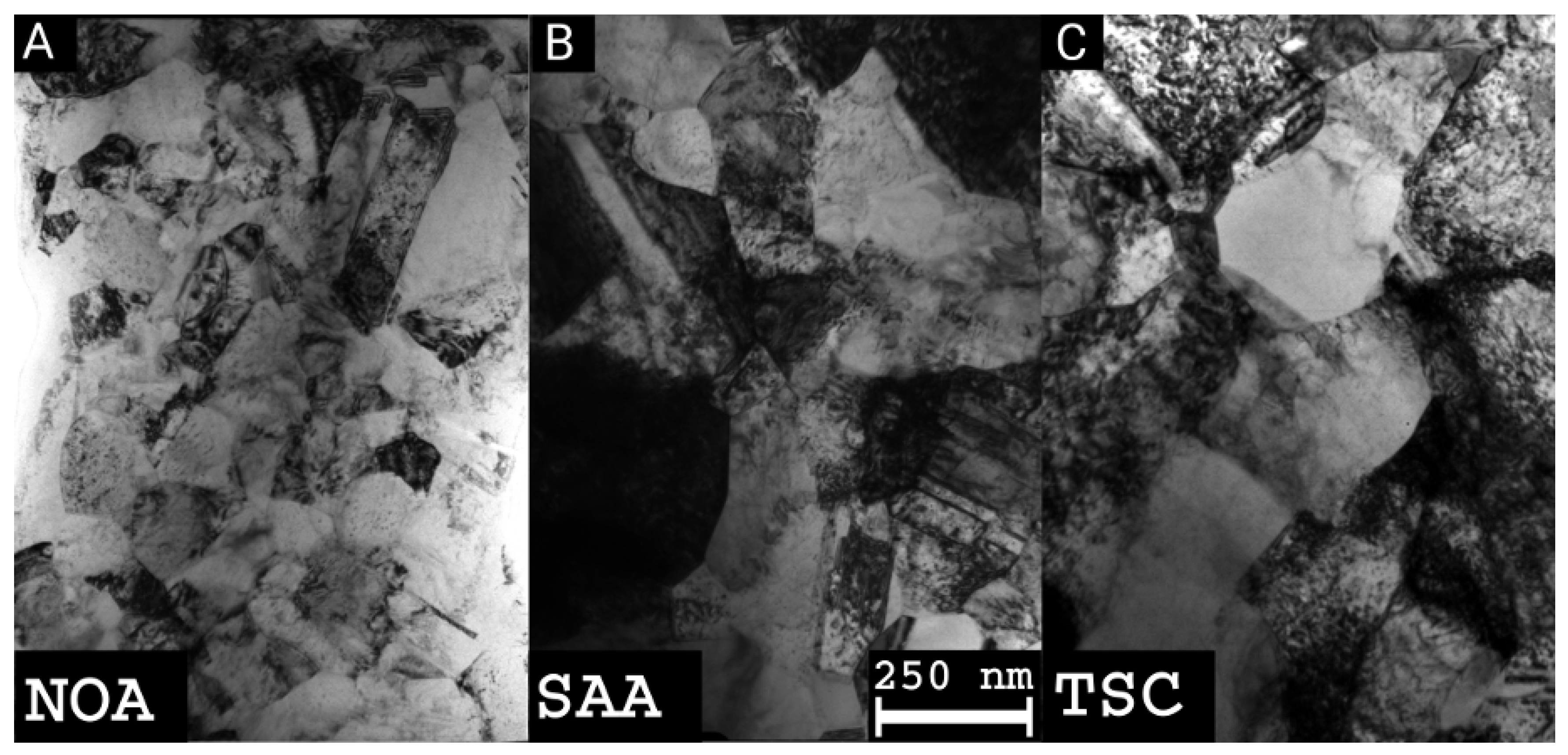
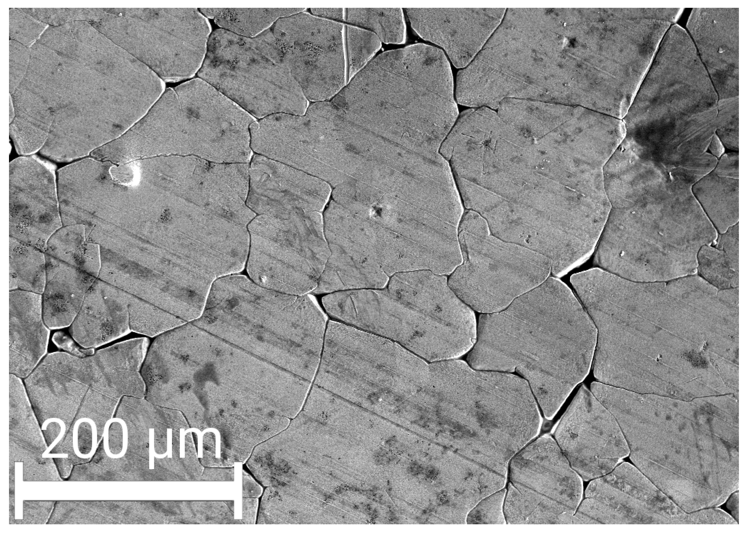
3.1. Evolution of the Crystallite and Grain Sizes, as Well as the Defect Density, during Annealing
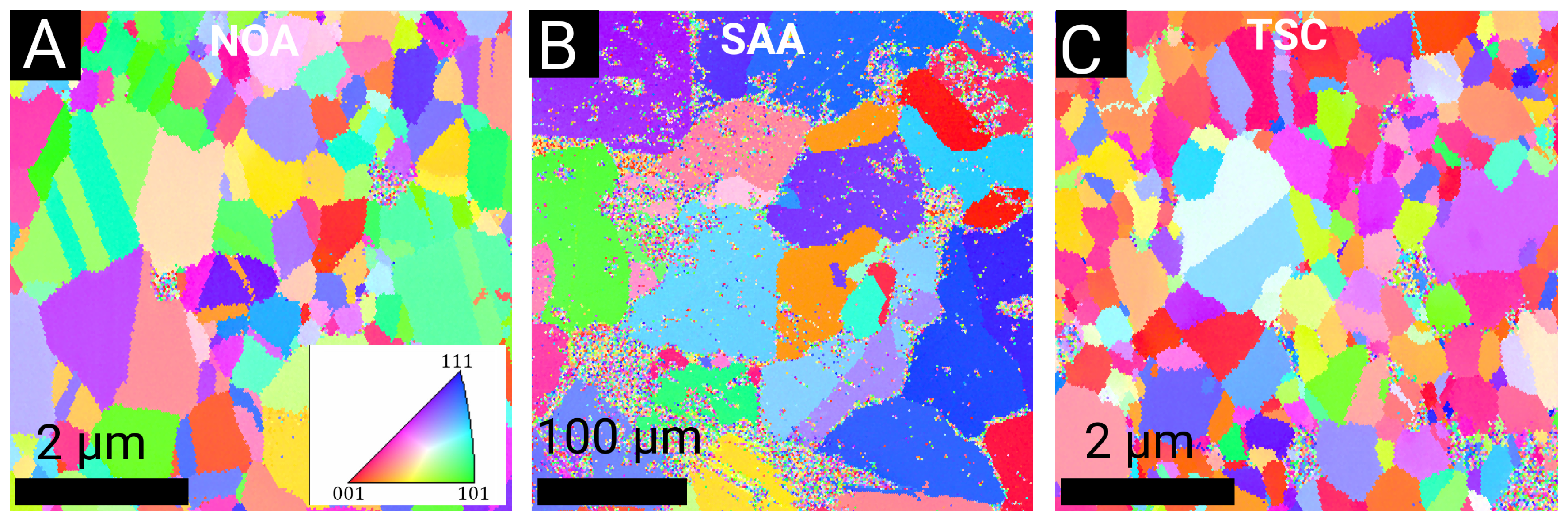
The changes in the dislocation density and the crystallite size determined by XLPA are shown in Figure 1 and Figure 2, respectively. The data are also listed in Table 2. Sample NOA had a stable crystallite size (∼33–40 nm) up to 600 K, however, between 600 and 1000 K the crystallite size increased to ∼151 nm. The dislocation density showed a stability with the value of ∼ 15 × 10 14 m−2 up to 500 K. Between 500 K and 1000 K, the dislocation density decreased to ∼ 2 × 10 14 m−2. Significant twin fault probability was not detected for both the initial and the annealed NOA specimens. The addition of trisodium citrate to the bath did not yield either a considerable twin fault probability or change of the crystallite size (∼38 nm). At the same time, the dislocation density (∼ 31 × 10 14 m−2) was about twice the value obtained for the additive-free sample. Sample TSC did not show significant change in the crystallite size up to 600 K. At the same time, the dislocation density decreased from ∼ 31 × 10 14 m−2 to ∼ 10 × 10 14 m−2 during the heat treatment up to 500 K (see Table 2). Between 500 and 1000 K, a considerable change in the dislocation density was not observed while the crystallite size increased from ∼39 to 152 nm (see Figure 2). The addition of saccharin to the bath increased the dislocation density by one order of magnitude to ∼ 180 × 10 14 m−2 compared to sample NOA, while leading to a decrease of the crystallite size down to ∼24 nm and to the formation of a considerable amount of twin faults (the twin fault probability was ∼3.6%). Sample SAA showed a stable crystallite size value of ∼24 nm up to 500 K while between 500 and 750 K the crystallite size increased to ∼73 nm. At 1000 K, the average crystallite size could not be determined by XLPA as its value was higher than the detection limit of XLPA for the applied diffraction configuration (∼800 nm). The dislocation density decreased from ∼ 180 × 10 14 m−2 to about 118 × 10 14 m−2 even during annealing to 400 K (see Figure 1). A second large decrease in the dislocation density was observed between 600 and 750 K. At the latter temperature, the dislocation density was only ∼ 6 × 10 14 m−2. The twin fault probability continuously decreased from ∼3.6% to zero when the temperature increased to 750 K (see Table 2). For the annealing temperature of 1000 K, XLPA was not able to determine the parameters of the microstructure as the peak breadth was very close to the instrumental broadening. In addition, the Debye-Scherrer diffraction rings obtained by XRD were spotty, suggesting a recrystallization at 1000 K.
The grain structures of the as-deposited layers are illustrated with the TEM images shown in Figure 3. The average grain size of the as-deposited NOA sample was about 105 nm (see Table 2). The addition of trisodium citrate did not yield a significant change in the average grain size. At the same time, saccharin resulted in a considerable decrease of the grain size to ∼32 nm. Significant change in the crystallite size during annealing did not occur at the temperatures lower than 750 K as shown by the XLPA investigations. Therefore, the grain size was investigated by microscopic methods only at 750 and 1000 K. Figure 4 shows TEM images taken on the samples annealed at 750 K. The average grain sizes obtained from the TEM images are listed in Table 2. It is noted that the grain sizes were determined from several images and the micrographs shown in Figure 4 are only illustrative examples. After the heat treatment at 1000 K, the grain size was studied by EBSD as shown in Figure 5 and the corresponding mean grain size values are given in Table 2. It is revealed that in the sample NOA the grain size increased from about 105 nm to ∼240 nm at 750 K, and this size further increased to about 470 nm at 1000 K. For the layer deposited from the bath containing saccharin, the grain size increased by almost one order of magnitude from ∼32 to ∼237 nm due to annealing up to 750 K. The increase of the temperature to 1000 K resulted in a very large increase of the grain size to about 60 μm. In the case of sample TSC, the grain size raised from ∼90 to ∼377 nm due to the heat treatment up to the temperature of 750 K. Between 750 and 1000 K, the grain size further increased slightly to about 405 nm as revealed by EBSD.
Our previous papers [7,8] demonstrated that in the as-deposited samples the grain sizes obtained from TEM investigations also follow a log-normal distribution, similar to the crystallite size distribution [8]. After the heat treatments, almost all samples (NOA, TSC, and SAA) preserved the log-normal characteristics of the grain size distribution. This result was obtained from the comparison of the medians determined directly from the size distribution histograms and calculated indirectly from the mean and the standard deviation of the same size distribution using the formula valid for log-normal distribution (see [8]). The relative difference between the two medians was about 3% for most of the annealed samples, which indicated that the grain size distribution can be satisfactorily characterized by a log-normal function. Pearson’s chi-square test [37] was also applied to check the log-normal nature of the grain size distributions. In this method, a probability was determined for the assumption that the experimental size distribution follows a log-normal function with the median and log-normal variance calculated from the experimentally determined mean and standard deviation. It was found that these probabilities were between 95.3–99.7% for most of the annealed samples. A detailed description of the evaluation procedure can be found in [8].
It should be noted, however, that there were two annealed samples which did not exhibit log-normal grain size distribution. The first one is sample TSC750, which showed a bimodal grain size distribution (see Figure 6) with the modes of 62 and 414 nm. The second sample was the specimen SAA1000 where, beside the very large grains observed by EBSD (the mean size was 60 μm), small grains with the size of 10–20 nm were also revealed by TEM/SAED (see Figure 7). However, the fraction of the nanocrystalline areas was very small as compared to the coarse-grained regions. EDS measurements were performed in TEM on the coarse-grained and nanocrystalline regions of the sample SAA1000 to determine the difference in the incorporating sulfur concentration in the two areas. Significantly higher sulfur concentration was detected in the nanocrystalline parts of the microstructure. The results are discussed in Section 4.1. It should also be noted that sample SAA1000 was fragmented, as shown in Figure 8. The EBSD image in Figure 5B suggests that each fragment in Figure 8 corresponds to one large grain, i.e., annealing at 1000 K resulted in cracking along the grain boundaries.

3.2. Texture

Pole figure measurements were performed before and after the heat treatments at the Bragg angles corresponding to reflections 111, 200 and 220. According to [8] the as-deposited samples NOA and TSC had (110) and (100) type out-of-plane fiber textures, respectively, while the as-received layer SAA had no considerable crystallographic texture. Figure 9 shows that in the case of samples NOA and TSC, the original textures were preserved or even became sharper during annealing. At the same time, the as-deposited sample SAA was free of texture; however, during the heat treatment up to 750 K, a mixed (111) and (100) fiber texture was developed. After annealing at 1000 K, the grain size became very large (60 μm laterally); therefore, the number of grains in the X-ray beam was reduced significantly. If we consider that the sample thickness is only 20 μm and the diameter of the sample was about 5 mm due to the limited size of the DSC sample holder, the number of grains contributing to the texture measurement was only about 100. Thus, in sample SAA1000 the grains had low number, large size and nearly defect-free interiors; therefore, the reflected X-ray peaks were very narrow. Since the pole figure experiment was carried out with a finite step size of 3 degrees and the scattered beam was very narrow, the reflected X-rays might not be detected in the texture measurement for layer SAA1000. This may explain the lack of considerable intensity in the pole figures taken on sample SAA1000.

3.3. Hardness

The different annealing-induced evolutions of the microstructures of the three studied layers may influence the change of the hardness during the heat treatments. Figure 10 shows the hardness values versus the annealing temperature. For sample NOA, the hardness remained practically unchanged up to 750 K (∼2300 MPa), then it decreased to ∼1300 MPa at 1000 K, which corresponds to 56% of the initial hardness. The initial hardness of sample TSC was higher (∼3300 MPa) than that for layer NOA, however, a continuous decrease of the hardness was observed for the former sample with increasing temperature (see Figure 10). The final hardness of sample TSC1000 was ∼2000 MPa (see Table 2), which is close to the initial hardness of NOA. This means that the addition of trisodium citrate to the bath is beneficial for the high-temperature hardness of Ni layers. In the case of sample TSC, the hardness decreased to 61% of the initial value. The addition of saccharin resulted in an increase of the initial hardness to about 5900 MPa. Only slight changes of the hardness were observed up to 600 K (see Figure 10). Above 600 K, a fast decrease of the hardness was observed. The final hardness of the sample SAA1000 was ∼1000 MPa, which is only 17% of the initial hardness, i.e., the addition of saccharin, through the incorporation of sulfur, reduced the thermal stability of the hardness of Ni electrodeposits.

4. Discussion

4.1. Effect of Additives on the Thermal Stability of the Nanostructure

Our former study [8] showed that the bath additives have a significant effect on both the grain size and the defect density in Ni electrodeposits. While trisodium citrate has no influence on the grain size, sulfur codeposition (from saccharin) in sample SAA reduced the grain size from ∼105 to ∼32 nm. This effect can be explained by the adsorption of the organic molecules/ions at the preferential near-equilibrium growth sites of the already formed crystals; therefore, rather new grains are nucleated, leading to grain refinement. At the same time, sulfur impurities in sample SAA resulted in an increase of the dislocation density. For nanocrystalline materials, it is usually assumed that the majority of dislocations can be found at the grain and subgrain boundaries. These dislocations may reduce the incompatibility stresses developed between the grains. Therefore, the highest dislocation density observed for sample SAA is due to its smallest grain size among the studied materials. It should be noted, however, that for layer TSC the grain size is only slightly smaller while the dislocation density is much higher than for sample NOA, suggesting that there is no strict correlation between the grain size and the dislocation density. The addition of saccharin to the bath also resulted in a considerable twin fault probability, which was explained by the codeposition of sulfur on planes (111) as discussed in detail in [8].
Table 2 reveals that the different microstructures and impurity contents of samples NOA, TSC, and SAA lead to different thermal stabilities of the nanostructures. There are two competing effects of the bath additives on the stability during annealing. First, additives yield a higher defect (grain boundary, dislocation, and twin fault) density in the as-deposited layers, which then causes a higher thermodynamic driving force for recovery and recrystallization; thereby reducing the stability during annealing. At the same time, impurities may impede the motion of defects during heat treatments, leading to a more difficult recovery and recrystallization. i.e., to a better stability. The addition of saccharin and trisodium citrate to the bath resulted in a higher density of lattice defects, such as dislocations and twin faults, which increased the thermodynamic driving force for recovery and recrystallization during annealing. Therefore, layers SAA and TSC were less stable than sample NOA up to the temperature of 500 K. The much higher defect density and the smaller grain size in specimen SAA compared to layer NOA resulted in a recrystallization at 1000 K while only recovery was observed in samples NOA and TSC. It seems that although layer SAA contains a considerable amount of sulfur, the stabilization effect was outperformed by the high driving force for structural relaxation, leading to a worse thermal stability as compared to the additive-free sample NOA (see Table 2). Therefore, a strong recrystallization occurred in layer SAA1000, resulting in a two orders of magnitude higher grain size than that for sample NOA. Specimen TSC exhibited a slightly better thermal stability as compared to layer NOA, which can be explained by the sharp (100) type texture of the former sample. Indeed, former studies proved that the initial texture has a significant effect on the grain growth during annealing [38,39,40,41]. Namely, it was revealed that the sharper the texture, the slower the grain coarsening during heat treatments [38]. This effect can be understood if we consider that the sharper texture in sample TSC is most probably accompanied by a lower average misorientation between the neighboring grains. Thus, the energy stored in the grain boundaries is lower, thereby stabilizing the microstructure of layer TSC at high temperatures. As the grain boundary misorientation has a distribution in the sample, this stabilizing effect is inhomogeneous in the layer, resulting in a bimodal grain size distribution at 750 K.
A heterogeneous grain structure was also observed in sample SAA1000. Namely, beside the large grains with the size of about 60 μm, very small (10–20 nm) grains remained in the microstructure. EDS measurements performed in TEM revealed that the region with nanosized grains in sample SAA1000 (see Figure 7A) was richer in sulfur than the neighboring large grain. Namely, the sulfur content was 50% higher in the nanocrystalline region than in the coarse grain. This observation suggests that the recrystallization occurred inhomogeneously in sample SAA. It is noted that the volume fraction of the remaining nanocrystalline regions is small as suggested by the EBSD image in Figure 5B and the spotty Debye-Scherrer rings obtained during XLPA experiments. Most probably, the segregation of sulfur impurities to the grain boundary regions is the main reason of the observed cracking along the grain boundaries upon annealing (see Figure 8).

4.2. Effect of Additives on Texture Evolution

The effect of additives on the texture formation during electrodeposition has already been discussed in detail in [8]. Briefly summarizing, in the additive-free Ni layer (sample NOA), the energy of planes 110 in the growing crystals was significantly reduced due to hydrogen codeposition as compared to other planes [42]. Therefore, a (110) type fiber texture was formed in the as-deposited sample. The addition of trisodium citrate to the bath decreased the rate of hydrogen gas detachment from the layer surface and the sodium presenting in the electrolyte changed the energies of the crystal surfaces which effect depended on the Miller indices [43]. Thus, the texture changed to 100 type in the as-deposited specimens TSC. The addition of saccharin to the bath resulted in the codeposition of sulfur in layer SAA. The strong covalent bond between Ni and S and its preferred bonding angles increased the probability of formation of grain boundaries, thereby leading to a reduced grain size and the elimination of texture [44].
During annealing of samples NOA and TSC, the initial type of texture did not change or even became sharper (see Figure 9) as the preferred orientations of the crystallites were inherited from the as-deposited state. At the same time, for layer SAA the texture-free microstructure became textured with combined 111 and 100 preferred orientations. This change can be explained by the depletion of the recovered/recrystallized grains from sulfur impurities. Then, this element does not influence the orientation of the growing new grains. Therefore, at the surface of the layer, those grains will grow preferably which have the lowest surface energy. In accordance with the surface energy anisotropy of nickel, the order of formation rate of crystalline planes is (111)>(100)>(110) [45]. Therefore, a mixed texture of (111) and (100) was observed in the recovered/recrystallized sample SAA.

4.3. Correlation between the Microstructure and the Hardness for the Annealed Layers

The thermal stability of the three electrodeposited Ni samples was also characterized by monitoring the hardness evolution versus the annealing temperature. The hardness variation reflects the difference in the thermal stability of the three nanostructures. For instance, after annealing at 1000 K, sample SAA1000 had the lowest hardness (∼1000 MPa) among the three layers due to the strongly recrystallized microstructure (see Table 2). At the same time, the hardness of specimen TSC1000 remained as high as ∼2000 MPa. This value is much higher than the hardness obtained for specimens NOA (∼1300 MPa) and SAA at 1000 K. In addition, the relative remaining hardness at 1000 K was 56%, 17%, and 61% for the films NOA, SAA, and TSC, respectively. Therefore, the hardness differences also show that the addition of SAA and TSC decreased and increased the thermal stability of electrodeposited Ni films, respectively.
Our former paper [8] suggested that the Vickers hardness (HV) of the nanocrystalline Ni layers deposited with different bath compositions can be described by the Hall–Petch relationship:
H V = H V 0 + k · d 1 / 2
where H V 0 is a threshold hardness with the value of 1707 ± 402 MPa, d is the average size of grains, and k is constant with the value of 9400 ± 2372 MPa·nm 1 / 2 . It should be noted that for the layers where the average twin spacing was smaller than the mean grain size, the former quantity was used as d since the strengthening of the twin faults [46] is very similar to the hardening of the general grain boundaries. The twin fault spacing can be calculated from the twin fault probability as 100 · d 111 / β , where d 111 is the lattice spacing for planes 111 and β is the twin fault probability in percentage. Figure 11 shows the Hall–Petch plot of the previously published data for the as-deposited layers produced with saccharin, trisodium citrate and formic acid additives as well as from Watts-type bath [8]. This plot was complemented with the data measured on the annealed samples of the present work (indicated by open symbols). In the as-deposited layers, the grain size was 100 nm or smaller while in the annealed deposits the grain size was higher than 100 nm. Former studies (e.g., [47,48,49]) have shown that the hardness versus grain size relationship can be described with different Hall–Petch parameters in the nanocrystalline and the coarse-grained regimes. Therefore, the data of the coarse-grained samples ( d 100 nm) were fitted with a separate straight line as shown in Figure 11. This fitting yielded H V 0 = 945 ± 119 MPa and k = 18,400 ± 3360 MPa·nm 1 / 2 . This result suggests that the Hall–Petch slope is smaller for the nanocrystalline Ni layers as compared to their coarse-grained counterparts. This observation is in accordance with former results in the literature [47,48,49]. The smaller slope for the grain sizes lower than 100 nm was attributed to the grain size dependence of the stress required to operate a Frank-read source and/or the increased contribution of deformation mechanisms occurring at the grain boundaries. Nevertheless, Figure 11 reveals that the decrease of the hardness during annealing can be ascribed mainly to the increase of the grain size.
It should be noted, however, that there are hardness variations during annealing which cannot be attributed solely to the changes of the grain size. For instance, the hardness of sample NOA750 agrees within the experimental error with the value obtained on the as-deposited layer NOA, although the grain size increased by a factor of 2.3 during annealing to 750 K. This apparent contradiction can be explained by the plastic deformation induced by hardness testing. The pressing of the indenter tip into the surface of the tested material causes a deformation with a plastic strain of about 8% [50]. This deformation can harden the annealed material to a similar level as observed for the as-deposited layer. In addition, sample SAA showed a slight strengthening during annealing to 500 K while the crystallite size did not change and the density of lattice defects (dislocations and twin faults) considerably decreased. Similar annealing-induced hardening effect was observed for nanocrystalline Ni and Ni-Mo electrodeposits in some recently published papers [23,51,52,53,54]. These former studies suggested that annealing at a moderate temperature (at the homologous temperatures of about 0.3–0.4) can yield grain boundary relaxation and segregation of impurities to grain boundaries which retard the deformation processes occurring in the grain boundaries in nanocrystalline materials (e.g., grain boundary sliding). For sample SAA, these deformation mechanisms may be important processes due to the very small grain size (∼30 nm). At the same time, for layers NOA and TSC, the grain size was much larger (∼100 nm); therefore, the changes in the grain boundary structure during low temperature annealing did not result in observable hardening.

5. Conclusions

An investigation was conducted to evaluate the effect of bath additives on the thermal stability of the microstructures in nanocrystalline Ni films processed by electrodeposition. Three samples were manufactured from a nickel sulfate based electrolyte: one layer without organic additives and two films with the addition of saccharin and trisodium citrate. The thermal stability of the three samples was studied in the temperature range of 300–1000 K. The following conclusions were drawn from the results:
  • Both saccharin and trisodium citrate increased the lattice defect density, but this effect was more pronounced in the former case. In addition, saccharin also reduced the grain size. Thus, the addition of saccharin strongly increased the stored energy in Ni films, which resulted in a higher thermodynamic driving force for the destabilization of the microstructure during annealing, leading to a recrystallization at 1000 K. The recrystallization in sample SAA yielded a decrease by three orders of magnitude in the defect density and a similar increase in the grain size. Trisodium citrate also increased the energy stored in dislocations; however, this effect was exceeded by the microstructure stabilization effect of the sharp texture. Therefore, sample TSC showed a better thermal stability as compared to the additive-free layer.
  • The recrystallization in sample SAA was inhomogeneous, i.e., between the large recrystallized grains nanocrystalline regions remained after annealing at 1000 K. The sulfur concentration in the nanocrystalline regions was higher than in the recrystallized large grains. This observation suggests that these impurities diffused from the recrystallized grains into the neighboring fine-grained regions where they stabilized the remaining nanostructure even at 1000 K.
  • The relative remaining hardness at 1000 K was 56%, 17%, and 61% for the samples NOA, SAA, and TSC, respectively. Thus, the hardness evolution during annealing also showed that the addition of saccharin and trisodium citrate decreased and increased the thermal stability of electrodeposited Ni films, respectively. The first effect is more pronounced than the second one. The Hall–Petch slope for the annealed samples was higher than that for the as-deposited layers due to the higher grain size. Nevertheless, the decrease of the hardness during annealing can be ascribed mainly to the increase of the grain size. On the other hand, some hardness changes cannot be explained by the variation of the grain size. For instance, the hardness of sample SAA increased during annealing up to 500 K, although the crystallite size did not change and the defect density decreased. This annealing-induced hardening can be explained by the reduced grain boundary sliding due to grain boundary relaxation and impurity segregation during annealing. Annealing-induced hardening was not observed for samples NOA and TSC due to their larger grain sizes.

Author Contributions

Formal analysis, T.K.; investigation, T.K.; resources, L.P., Z.C. and J.G.; writing—original draft preparation, T.K. and J.G.; writing—review and editing, all of the authors; visualization, T.K. and J.G.; supervision, J.G. and Z.C.; funding acquisition, J.G.

Funding

This work was supported in part by the Ministry of Human Capacities of Hungary within the ELTE University Excellence program (1783-3/2018/FEKUTSRAT).

Conflicts of Interest

The authors declare no conflict of interest.

References

  1. Meyers, M.A.; Mishra, A.; Benson, D.J. Mechanical properties of nanocrystalline materials. Prog. Mater. Sci. 2006, 51, 427–556. [Google Scholar] [CrossRef]
  2. Kumar, K.S.; Swygenhoven, H.V.; Suresh, S. Mechanical behavior of nanocrystalline metals and alloys. Acta Mater. 2003, 51, 5743–5774. [Google Scholar] [CrossRef]
  3. Kumar, K.S.; Suresh, S.; Chisholm, M.F.; Horton, J.A.; Wang, P. Deformation of electrodeposited nanocrystalline nickel. Acta Mater. 2003, 51, 387–405. [Google Scholar] [CrossRef]
  4. Torre, F.D.; Swygenhoven, H.V.; Victoria, M. Nanocrystalline electrodeposited Ni: Microstructure and tensile properties. Acta Mater. 2002, 50, 3957–3970. [Google Scholar] [CrossRef]
  5. Budrovic, Z.; Swygenhoven, H.V.; Derlet, P.M.; Petegem, S.V.; Schmitt, B. Plastic Deformation with Reversible Peak Broadening in Nanocrystalline Nickel. Science 2004, 304, 273–276. [Google Scholar] [CrossRef] [PubMed]
  6. Schwaiger, R.; Moser, B.; Dao, M.; Chollacoop, N.; Suresh, S. Some critical experiments on the strain-rate sensitivity of nanocrystalline nickel. Acta Mater. 2003, 51, 5159–5172. [Google Scholar] [CrossRef]
  7. Kolonits, T.; Jenei, P.; Tóth, B.G.; Czigány, Z.; Gubicza, J.; Péter, L.; Bakonyi, I. Characterization of Defect Structure in Electrodeposited Nanocrystalline Ni Films. J. Electrochem. Soc. 2016, 163, D107–D114. [Google Scholar] [CrossRef]
  8. Kolonits, T.; Jenei, P.; Péter, L.; Bakonyi, I.; Czigány, Z.; Gubicza, J. Effect of bath additives on the microstructure, lattice defect density and hardness of electrodeposited nanocrystalline Ni films. Surf. Coat. Technol. 2018, 349, 611–621. [Google Scholar] [CrossRef]
  9. Gertsman, V.Y.; Birringer, R. On the room-temperature grain growth in nanocrystalline copper. Scr. Metall. Mater. 1994, 30, 577–581. [Google Scholar] [CrossRef]
  10. Klement, U.; Erb, U.; El-Sherik, A.M.; Aust, K.T. Thermal stability of nanocrystalline Ni. Mater. Sci. Eng. A 1995, 203, 177–186. [Google Scholar] [CrossRef]
  11. Dake, J.M.; Krill, C.E. Sudden loss of thermal stability in Fe-based nanocrystalline alloys. Scr. Mater. 2012, 66, 390–393. [Google Scholar] [CrossRef]
  12. Ames, M.; Markmann, J.; Karos, R.; Michels, A.; Tschope, A.; Birringer, R. Unraveling the nature of room temperature grain growth in nanocrystalline materials. Acta Mater. 2008, 56, 4255–4266. [Google Scholar] [CrossRef]
  13. Burzyńska, L.; Rudnik, E.; Koza, J.; Błaż, L.; Szymański, W. Electrodeposition and heat treatment of nickel/silicon carbide composites. Surf. Coat. Technol. 2008, 202, 2545–2556. [Google Scholar] [CrossRef]
  14. Broszeit, E. Mechanical, thermal and tribological properties of electro- and chemodeposited composite coatings. Thin Solid Films 1982, 95, 133–142. [Google Scholar] [CrossRef]
  15. Gyftou, P.; Stroumbouli, M.; Pavlatou, E.A.; Spyrellis, N. Electrodeposition of Ni/SiC Composites by Pulse Electrolysis. Trans. IMF 2002, 80, 88–91. [Google Scholar] [CrossRef]
  16. Wang, S.C.; Wei, W.C.J. Characterization of electroplated Ni/SiC and Ni/Al2O3 composite coatings bearing nanoparticles. J. Mater. Res. 2003, 18, 1566–1574. [Google Scholar] [CrossRef]
  17. Boylan, K.; Ostrander, D.; Erb, U.; Palumbo, G.; Aust, K.T. An in situ TEM study of the thermal stability of nanocrystalline NiP. Scr. Metall. Mater. 1991, 25, 2711–2716. [Google Scholar] [CrossRef]
  18. Chookajorn, T.; Murdoch, H.A.; Schuh, C.A. Design of stable nanocrystalline alloys. Science 2012, 337, 951–954. [Google Scholar] [CrossRef]
  19. Darling, K.A.; VanLeeuwen, B.K.; Semones, J.E.; Koch, C.C.; Scattergood, R.O.; Kecskes, L.J.; Mathaudhu, S.N. Stabilized nanocrystalline iron-based alloys: Guiding efforts in alloy selection. Mater. Sci. Eng. A 2011, 528, 4365–4371. [Google Scholar] [CrossRef]
  20. Choi, P.; da Silva, M.; Klement, U.; Al-Kassab, T.; Kirchheim, R. Thermal stability of electrodeposited nanocrystalline Co-1.1 at.% P. Acta Mater. 2005, 53, 4473–4481. [Google Scholar] [CrossRef]
  21. Chookajorn, T.; Schuh, C.A. Nanoscale segregation behavior and high-temperature stability for nanocrystalline W–20 at.% Ti. Acta Mater. 2014, 73, 128–138. [Google Scholar] [CrossRef]
  22. Darling, K.A.; VanLeeuween, B.K.; Koch, C.C.; Scattergood, R.O. Thermal stability of nanocrystalline Fe–Zr alloys. Mater. Sci. Eng. A 2010, 527, 3572–3580. [Google Scholar] [CrossRef]
  23. Wang, Y.M.; Cheng, S.; Wei, Q.M.; Ma, E.; Nieh, T.G.; Hamza, A. Effects of annealing and impurities on tensile properties of electrodeposited nanocrystalline Ni. Scr. Mater. 2004, 51, 1023–1028. [Google Scholar] [CrossRef]
  24. Heuer, J.K.; Okamoto, P.R.; Lam, N.Q.; Stubbins, J.F. Relationship between segregation-induced intergranular fracture and melting in the nickel–sulfur system. Appl. Phys. Lett. 2000, 76, 3403–3405. [Google Scholar] [CrossRef]
  25. Hibbard, G.D.; McCrea, J.L.; Palumbo, G.; Aust, K.T.; Erb, U. An initial analysis of mechanisms leading to late stage abnormal grain growth in nanocrystalline Ni. Scr. Mater. 2002, 47, 83–87. [Google Scholar] [CrossRef]
  26. Xiao, C.; Mirshams, R.A.; Whang, S.H.; Yin, W.M. Tensile behavior and fracture in nickel and carbon doped nanocrystalline nickel. Mater. Sci. Eng. A 2001, 301, 35–43. [Google Scholar] [CrossRef]
  27. Lücke, K.; Detert, K. A quantitative theory of grain-boundary motion and recrystallization in metals in the presence of impurities. Acta Metall. 1957, 5, 628–637. [Google Scholar] [CrossRef]
  28. Michels, A.; Krill, C.E.; Ehrhardt, H.; Birringer, R.; Wu, D.T. Modeling the influence of grain-size-dependent solute drag on the kinetics of grain growth in nanocrystalline materials. Acta Mater. 1999, 47, 2143–2152. [Google Scholar] [CrossRef]
  29. Hillert, M. Inhibition of grain growth by second-phase particles. Acta Metall. 1998, 36, 3177–3181. [Google Scholar] [CrossRef]
  30. Gottstein, G.; Shvindlerman, L.S. Grain Boundary Migration in Metals: Thermodynamics, Kinetics, Applications, 2nd ed.; CRC Press: Boca Raton, FL, USA, 2010. [Google Scholar]
  31. Hondros, E.D.; Seah, M.P.; Hofmann, S.; Lejcek, P. Interfacial and surface microchemistry. In Physical Metallurgy, 4th ed.; Cahn, R.W., Haasen, P., Eds.; North-Holland: Amsterdam, The Netherlands, 1996; pp. 1202–1289. [Google Scholar]
  32. Tóth, B.G.; Péter, L.; Révész, A.; Pádár, J.; Bakonyi, I. Temperature dependence of the electrical resistivity and the anisotropic magnetoresistance (AMR) of electrodeposited Ni-Co alloys. Eur. Phys. J. B 2010, 75, 167–177. [Google Scholar] [CrossRef] [Green Version]
  33. Green, T.A.; Russell, A.E.; Roy, S. The Development of a Stable Citrate Electrolyte for the Electrodeposition of Copper-Nickel Alloys. J. Electrochem. Soc. 1998, 150, 875–881. [Google Scholar] [CrossRef]
  34. Barna, A. Topographic kinetics and practice of low angle ion beam thinning. Mater. Res. Soc. Symp. Proc. 1992, 254, 3–22. [Google Scholar] [CrossRef]
  35. Ribárik, G.; Gubicza, J.; Ungár, T. Correlation between strength and microstructure of ball-milled Al–Mg alloys determined by X-ray diffraction. Mater. Sci. Eng. A 2004, 387, 343–347. [Google Scholar] [CrossRef]
  36. Balogh, L.; Ribárik, G.; Ungár, T. Stacking faults and twin boundaries in fcc crystals determined by X-ray diffraction profile analysis. J. Appl. Phys. 2006, 100, 023512. [Google Scholar] [CrossRef]
  37. Pearson, K.X. On the criterion that a given system of deviations from the probable in the case of a correlated system of variables is such that it can be reasonably supposed to have arisen from random sampling. Lond. Edinb. Dublin Philos. Mag. J. Sci. Ser. 1900, 50, 157–175. [Google Scholar] [CrossRef]
  38. Novikov, V.Y. On computer simulation of texture development in grain growth. Acta Metall. 1979, 27, 1461–1466. [Google Scholar] [CrossRef]
  39. Abbruzzese, G.; Lücke, K. A theory of texture controlled grain growth-I. Derivation and general discussion of the model. Acta Metall. 1986, 34, 905–914. [Google Scholar] [CrossRef]
  40. Eichelkraut, H.; Abbruzzese, G.; Lücke, K. A theory of texture controlled grain growth-II. Numerical and analytical treatment of grain growth in the presence of two texture components. Acta Metall. 1988, 36, 55–68. [Google Scholar] [CrossRef]
  41. Abbruzzese, G.; Lucke, K.; Eichelkraut, H. Computer simulation of texture-controlled grain growth. Trans. Iron Steel Inst. Jpn. 1988, 28, 818–825. [Google Scholar] [CrossRef]
  42. Li, D.Y.; Szpunar, J.A. Textural evolution in electrodeposits under the influence of adsorbed foreign species: Part I textural evolution in iron electrodeposits affected by hydrogen co-deposition. J. Mater. Sci. 1997, 32, 5513–5523. [Google Scholar] [CrossRef]
  43. Wu, X.; Gao, Q.; Li, Z. Effects of additives on morphology and hydrogen evolution activities of nickel films prepared by electrodepositing. Int. J. Electrochem. Sci. 2015, 10, 8823–8833. [Google Scholar]
  44. Neurock, M.; van Santen, R.A. Theory of carbon-sulfur bond activation by small metal sulfide particles. J. Am. Chem. Soc. 1994, 116, 4427–4439. [Google Scholar] [CrossRef]
  45. Reddy, A.K.N. Preferred orientations in nickel electro-deposits I. The mechanism of development of textures in nickel electro-deposits. J. Electroanal. Chem. 1963, 6, 141–152. [Google Scholar]
  46. Lu, L.; Shen, Y.; Chen, X.; Qian, L.; Lu, K. Ultrahigh strength and high electrical conductivity in copper. Science 2004, 304, 422–426. [Google Scholar] [CrossRef] [PubMed]
  47. Erb, U. Electrodeposited nanocrystals: Synthesis, properties and industrial applications. Nanostruct. Mater. 1995, 6, 533–538. [Google Scholar] [CrossRef]
  48. Jeong, D.H.; Gonzalez, F.; Palumbo, G.; Aust, K.T.; Erb, U. The effect of grain size on the wear properties of electrodeposited nanocrystalline nickel coatings. Scr. Mater. 2001, 44, 493–499. [Google Scholar] [CrossRef]
  49. Shaw, L.L.; Ortiz, A.L.; Villegas, J.C. Hall–Petch relationship in a nanotwinned nickel alloy. Scr. Mater. 2008, 58, 951–954. [Google Scholar] [CrossRef]
  50. Tabor, D. The hardness and strength of metals. J. Inst. Met. 1951, 79, 1–18. [Google Scholar]
  51. Hu, J.; Shi, Y.N.; Sauvage, X.; Sha, G.; Lu, K. Grain boundary stability governs hardening and softening in extremely fine nanograined metals. Science 2017, 355, 1292–1296. [Google Scholar] [CrossRef]
  52. Kapoor, G.; Péter, L.; Fekete, E.; Lábár, J.L.; Gubicza, J. The influence of Mo addition on the microstructure and its thermal stability for electrodeposited Ni films. Mater. Charact. 2018, 145, 563–572. [Google Scholar] [CrossRef]
  53. Zheng, X.; Hu, J.; Li, J.; Shi, Y. Achieving ultrahigh hardness in electrodeposited nanograined Ni-based binary alloys. Nanomaterials 2019, 9, 546. [Google Scholar] [CrossRef] [PubMed]
  54. Gubicza, J. Annealing-induced hardening in ultrafine-grained and nanocrystalline materials. Adv. Eng. Mater 2019, 1900507. [Google Scholar] [CrossRef]
Figure 1. The dislocation density in logarithmic scale obtained by X-ray line profile analysis (XLPA) versus the heat treatment temperature. The curves are only for guidance and do not represent any fitting model.
Coatings 09 00644 g001
Figure 2. The crystallite size obtained by XLPA versus the heat treatment temperature. The curves are only for guidance and do not represent any fitting model.
Coatings 09 00644 g002
Figure 3. TEM images taken on samples NOA (A), SAA (B), and TSC (C) before heat treatments.
Coatings 09 00644 g003
Figure 4. TEM images taken on samples NOA (A), SAA (B), and TSC (C) after heat treatment at 750 K.
Coatings 09 00644 g004
Figure 5. EBSD orientation maps for samples NOA (A), SAA (B), and TSC (C) annealed up to 1000 K.
Coatings 09 00644 g005
Figure 6. Bimodal grain size distribution for sample TSC750.
Coatings 09 00644 g006
Figure 7. TEM images and selected-area electron diffraction (SAED) patterns for sample SAA1000. (A) TEM image of a fine-grained area at large magnification. (B) TEM image at lower magnification showing the coexistence of coarse-grained and fine-grained parts in the microstructure. The TEM image in (A) was taken within the area of the small green square. (C) The SAED pattern obtained from the fine-grained area shown (A), where only fcc diffraction rings are observable. (D) SAED pattern obtained from a larger area within the large red square in (B) which reveals both diffraction rings from fine-grained areas and diffraction spots from individual large grain(s). The arrows indicate the areas where the diffraction patterns and the high magnification image were taken.
Coatings 09 00644 g007
Figure 8. Secondary electron image in SEM for sample SAA1000. The cracks were formed at the grain boundaries.
Coatings 09 00644 g008
Figure 9. Pole figures for samples NOA, TSC, and SAA before and after heat treatments at different temperatures. For each sample, that pole figure was displayed which reflects best the evolved texture. Therefore, for specimens NOA and TSC, the pole figures (220) and (200) are shown, respectively. Sample SAA had no initial texture, but a mixed (111) and (200) fiber texture was developed during annealing.
Coatings 09 00644 g009
Figure 10. The Vickers microhardness of the three samples versus the temperature of the heat treatment. The curves are only for guidance and do not represent any fitting model.
Coatings 09 00644 g010
Figure 11. Hall–Petch plot of the hardness versus the inverse square root of the characteristic length in the microstructure (the lowest of the grain size and the twin fault spacing). The solid circles correspond to as-deposited nanocrystalline layers produced with different bath additives (the data were taken from [8]). The open circles show the data obtained on the annealed samples in this study and the new measurements. The straight lines fitted to the data corresponding to the grain sizes smaller and larger than 100 nm are also shown.
Coatings 09 00644 g011
Table 1. Composition of the electrolytes used for deposition. All components are measured in units (g/L). NOA = no organic additive; SAA = saccharin additive; TSC = trisodium citrate.
Component/SolutionNOASAATSCRole
NiSO4·6H2O155155185Ni source
H3BO31515-pH-buffer
NaSO4·10H2O9696-Supporting electrolyte
H3NO3S1010-wetting agent
Saccharin-1-additive
C7H5NO3S
Trisodium citrate--65additive
C6H5O7Na3·2H2O
Table 2. The grain size determined by transmission electron microscopy (TEM) (d), the crystallite size (<x>), the dislocation density ( ρ ) and the twin fault probability ( β ) obtained by XLPA and the hardness for the as-deposited and the heat treated samples. It is noted that for all layers heated up to 1000 K the grain size was determined by EBSD.
SampleTemperature (K)d (nm)<x> (nm)ρ (1014 m−2)β (%)HV (MPa)
NOAas-deposited105 ± 2633 ± 415 ± 20.02300 ± 180
NOA400-39 ± 814 ± 20.02400 ± 260
NOA500-38 ± 515 ± 20.02300 ± 280
NOA600-41 ± 87 ± 20.02100 ± 320
NOA750240 ± 2688 ± 93 ± 10.02400 ± 210
NOA1000470 ± 52151 ± 172 ± 10.01300 ± 260
SAAas-deposited32 ± 224 ± 3180 ± 203.65900 ± 300
SAA400-22 ± 3118 ± 153.16100 ± 360
SAA500-21 ± 2124 ± 151.06700 ± 350
SAA600-46 ± 6106 ± 100.25200 ± 300
SAA750237 ± 3073 ± 96 ± 20.02700 ± 190
SAA100060000 ± 20000>800<0.1<0.11000 ± 50
TSCas-deposited90 ± 1138 ± 531 ± 30.03300 ± 210
TSC400-44 ± 518 ± 20.03100 ± 740
TSC500-47 ± 510 ± 20.02800 ± 340
TSC600-39 ± 69 ± 20.02500 ± 300
TSC750377 ± 5862 ± 710 ± 20.02200 ± 220
TSC1000405 ± 49152 ± 167 ± 10.02000 ± 300

