Article

Effect of Thioacetamide Concentration on the Preparation of Single-Phase SnS and SnS2 Thin Films for Optoelectronic Applications

by
Sreedevi Gedi
1,†,
Vasudeva Reddy Minnam Reddy
1,†,
Salh Alhammadi
1,
Doohyung Moon
1,
Yeongju Seo
1,
Tulasi Ramakrishna Reddy Kotte
2,
Chinho Park
1 and
Woo Kyoung Kim
1,*
1
School of Chemical Engineering, Yeungnam University, 280 Daehak-ro, Gyeongsan 38541, Korea
2
Solar Energy Laboratory, Department of Physics, Sri Venkateswasra University, Tirupati 517 502, India
*
Author to whom correspondence should be addressed.
These authors contributed equally to this work.
Coatings 2019, 9(10), 632; https://doi.org/10.3390/coatings9100632
Submission received: 5 September 2019 / Revised: 26 September 2019 / Accepted: 27 September 2019 / Published: 30 September 2019
(This article belongs to the Special Issue Advanced Thin Film Materials for Photovoltaic Applications)

Abstract

:
Eco-friendly tin sulfide (SnS) thin films were deposited by chemical solution process using varying concentrations of a sulfur precursor (thioacetamide, 0.50–0.75 M). Optimized thioacetamide concentrations of 0.6 and 0.7 M were obtained for the preparation of single-phase SnS and SnS2 films for photovoltaic absorbers and buffers, respectively. The as-deposited SnS and SnS2 thin films were uniform and pinhole-free without any major cracks and satisfactorily adhered to the substrate; they appeared in dark-brown and orange colors, respectively. Thin-film studies (compositional, structural, optical, and electrical) revealed that the as-prepared SnS and SnS2 films were polycrystalline in nature; exhibited orthorhombic and hexagonal crystal structures with (111) and (001) peaks as the preferred orientation; had optimal band gaps of 1.28 and 2.92 eV; and exhibited p- and n-type electrical conductivity, respectively. This study presents a step towards the growth of SnS and SnS2 binary compounds for a clean and economical power source.

Graphical Abstract

1. Introduction

In recent years, inorganic semiconductors have been employed to generate clean energy in various optoelectronic and electrochemical fields, mainly because of their high stability under atmospheric conditions [1,2,3,4,5]. Among these, groups IV–VI tin-based binary sulfides such as tin monosulfide (SnS) and tin disulfide (SnS2) have drawn much attention because of their abundance, low cost, non-toxicity, high catalytic activity, material diversity, structural multiformity, and excellent electrical conductivity [6]. SnS crystallizes in an orthorhombic structure with the Pnma space group [7] and exhibits excellent optoelectrical properties such as a strong absorption coefficient (> 105 cm−1) with direct optical band gap energy ranging from 1.16 to 1.79 eV [8,9] and p-type conductivity with a carrier concentration of the order of 1011–1018 cm−3 [10], which are suitable for thin-film photovoltaic absorbers. In addition, maintenance of stoichiometry is simpler compared with the other conventional light absorbers [11,12,13,14,15]. Another tin-based binary sulfide, SnS2, adopts a hexagonal-layered structure with the P3ml space group, similar to the structure of the CdI2 system [16]. Moreover, SnS2 has a relatively high optical band gap in the range of 2.04–3.30 eV [17] with direct transitions and exhibits n-type conductivity. These promising characteristics make SnS a suitable absorber candidate material for thin-film solar cells [1]; moreover, SnS is presumably expected to be a better alternative to the already developed technologies such as Cu(In,Ga)Se2 (23.35%) [18] and CdTe (22.1%) [19], which are limited by their toxicity, scarcity, and exorbitant cost. Similarly, the favorable electronic characteristics, excellent structural flexibility, wider spectral response, and better thermal stability of SnS2 make it a competitive nontoxic substitute for the conventional CdS [14] and Zn(O,S) [20] buffers in thin-film solar cells [2]. Furthermore, both SnS and SnS2 have also been applied in photodetectors [21,22], photocatalysis [23], water splitting [24], gas sensors [25,26], biosensors [27], field-effect transistors [28,29], lithium-sodium ion batteries [30,31], thermoelectrics [32], electrochemical capacitors [33], and supercapacitors [34].
Various approaches including physical and chemical techniques have been explored to deposit both SnS and SnS2 thin films. Among these techniques, the chemical solution process (CSP) or chemical bath deposition (CBD) offers more inexpensive and flexible depositions. The preparation of single-phase SnS and SnS2 films by CSP depends on the release and reaction rate of sulfur ions in the reaction solution, which can be controlled by the selection of a suitable sulfur precursor at a concentration, which affects not only the formation of the phase but also the growth rate, thickness, and other physical properties of the product films. Therefore, optimizing the concentration of the sulfur precursor is highly preferable to obtain high-quality SnS and SnS2 films for the desired applications. Previous research suggests that thioacetamide (TA) and sodium thiosulfate have been mainly used as sulfur precursors since 1987 (Figure 1). Of these, thioacetamide is more preferable because it works under both acidic and alkaline bath conditions.
Therefore, a set of SnS thin films were deposited by CSP using varying thioacetamide concentrations, while the other growth parameters were maintained constant. The influence of thioacetamide concentration on the growth and physical properties of the thin films are discussed in the subsequent sections. Thus, its concentration was optimized for the preparation of pure SnS and SnS2 films for wide applications.

2. Experimental Section

The deposition procedure for SnS and SnS2 films by CSP is schematically presented in Figure 2, and the process has been described in detail in our previous reports [35,36]. Analytical-grade tin chloride (SnCl2.2H2O, 0.1 M) and tartaric acid (C4H6O6, 1.2 M) were used as a tin source and complexing agent, respectively, and 10 mL of thioacetamide (C2H5NS, 0.50-0.75 M) was used as the source material for the S ions. The as-prepared thin films were cleaned using deionized (DI) water and dried in a vacuum oven. By the following equations, the kinetics of SnS and SnS2 films can be understood.
In an aqueous tin chloride solution, the complexation of tartaric acid is
SnCl2∙2H2O + L ⇔ Sn(C4H6O6)2+ + 2Cl + 2H2O.
The free Sn2+ ions are slowly released by the dissociation of tin tartrate ions (Sn(C4H6O6)2+) in a controlled way, as below:
Sn(C4H6O6)2+ ⇌ Sn2+ + C4H6O6.
The hydrolysis of thioacetamide can produce S2− ions by
CH3CSNH2 + H2O ⇌ CH3CONH2 + H2S,
H2S + H2O ⇌ H3O+ + HS,
HS ⇌ H+ + S2−,
HS + OH ⇌ H2O + S2−.
When the thioacetamide concentration is changed, multiphase or other single-phase films can be formed by the following reactions:
Sn2+ + S2− → SnS,
3SnS + S → SnS + Sn2S3,
Sn2S3 + S → 2SnS2,
The compositional, structural, optical, and electrical characteristics of the as-deposited films were analyzed using an X-ray photoelectron spectrometer (Waltham, MA, USA) (XPS: A VG Multilab 2000; Al Kα radiation = 1486.6 eV), X-ray diffractometer (Almelo, Overijssel, Netherlands) (XRD: PANalytical X’Pert PRO MPD, Malvern Panalytical with Cu Kα radiation, λ = 1.5406 Å), UV-Vis-NIR spectrometer (Santa Clara, CA, USA) (Aglient), and Hall measurement system (Anyang-city, Gyeonggi-do, South Korea) (ECOPIA HMS-3000VER), respectively.

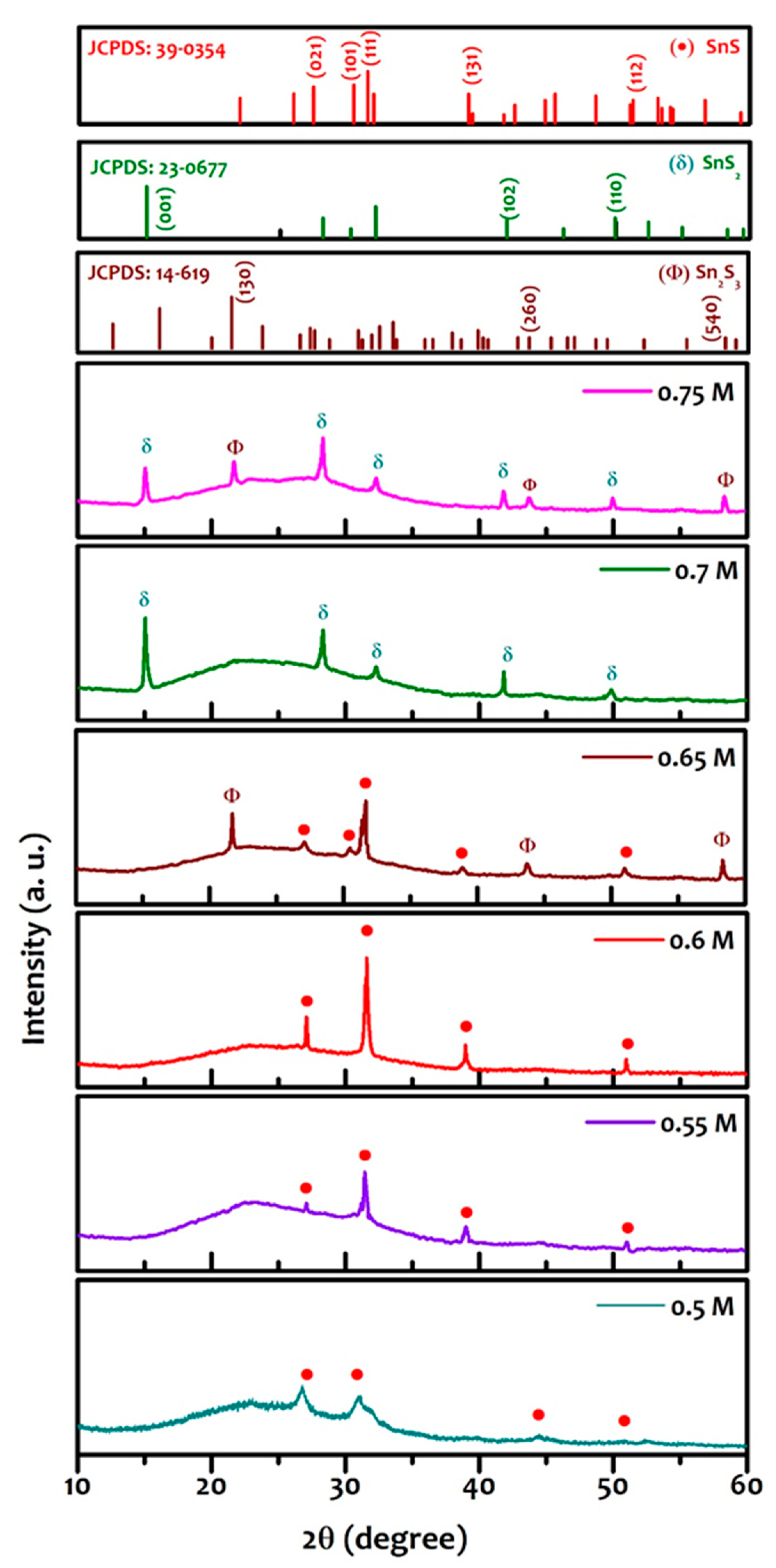
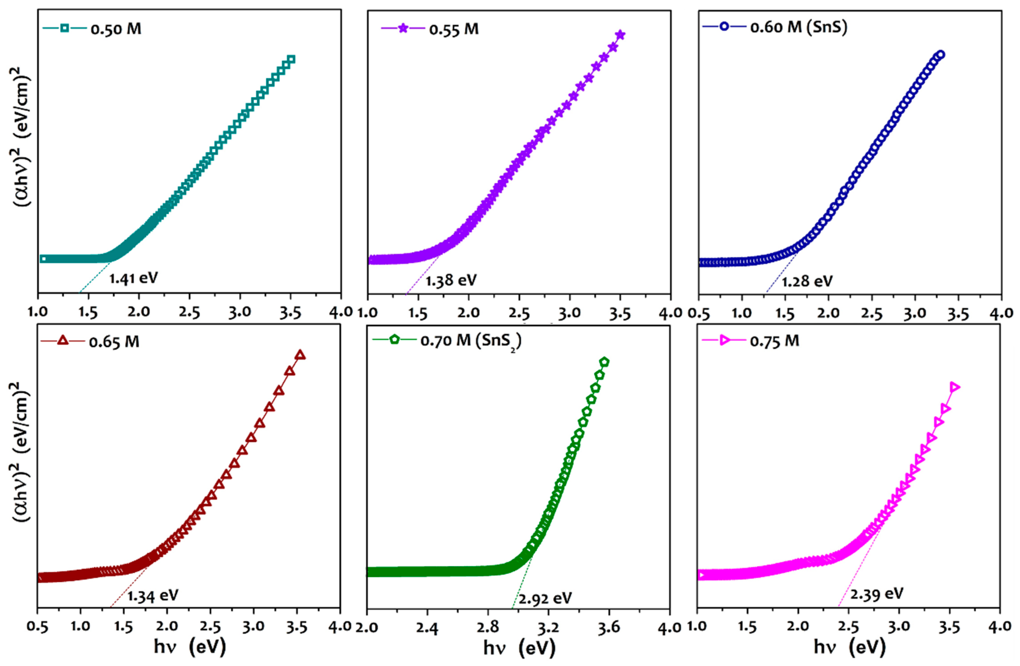
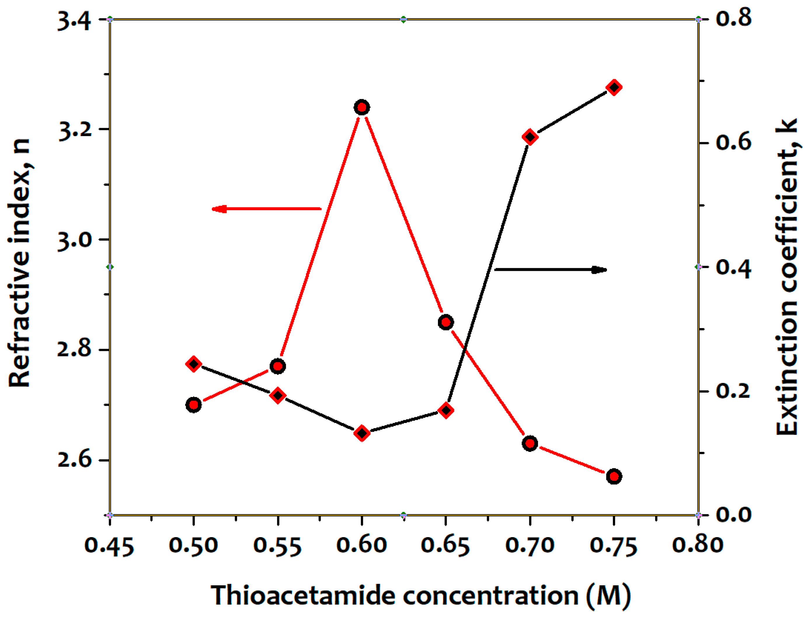
3. Results and Discussion

All the deposited tin sulfide films were confirmed to be satisfactorily adherent. The films appeared in dark-brown and orange shades at TA concentration ranges of 0.50−0.65 M and 0.70−0.75 M, respectively. The effect of TA concentration on the elemental composition and chemical states of elements was investigated by XPS. The XPS survey spectrum indicated that the deposited films were mainly composed of the Sn 3d doublet along with the S 2p peaks, representing the existence of the elements Sn and S. A high-resolution scan of the Sn 3d and S 2p peaks is shown in Figure 3a,b, respectively.
The Sn 3d doublet in the films grown with lower TA concentrations (0.5–0.6 M) showed two strong peaks at about 485.6 and 494.1 eV that were related to Sn 3d5/2 and Sn 3d3/2, respectively, which are the characteristics of Sn2+ in SnS. The Sn 3d5/2 and Sn 3d3/2 peaks were observed to expand at a TA concentration of 0.65 M, and the deconvolution of these peaks reveals the existence of two humps in each peak, linked to the elevated intensity for Sn2+ and low intensity for Sn4+, indicating the coexistence of secondary Sn2S3 along with SnS. As the TA concentration was increased further (0.7 M), the spectra showed the binding energies for Sn 3d5/2 and Sn 3d3/2 as 486.7 (487.2) and 494.9 (495.1) eV, respectively [37,38], revealing the presence of Sn4+ produced in the SnS2 phase. Beyond this concentration (0.75 M), the deconvolution of the broadened Sn 3d doublets suggests the presence of low intense Sn2+ and high intense Sn4+, confirming the formation of the Sn2S3 secondary phase along with SnS2. The high-resolution XPS spectrum of S 2p for the as-prepared films exhibited single peaks related to S2−–Sn2+ (161.3 eV) and S–Sn4+ (162.3 eV) bonds at TA concentrations of 0.5–0.6 and 0.7 M, which are characteristic of single-phase SnS and SnS2 films, respectively [35]. The remaining core-level S 2p spectra (for TA = 0.65 and 0.75 M) showed two deconvoluted peaks related to the binding energies of both S2−–Sn2+ (161.3 eV) and S–Sn4+ (162.3 eV) bonding, suggesting the presence of the Sn2S3 secondary phase. The Sn/S atomic ratio varied between 1.12 to 0.53 with the change in TA concentration. The lower Sn/S atomic ratio indicated that S is more dominant at higher TA values. This excess of sulfur probably led to the formation of the binary phases, SnS2 and Sn2S3 along with the SnS phase, which were further observed in the XRD studies. The film grown at TA concentrations of 0.6 M and 0.7 M exhibited Sn/S atomic ratios of 0.98 and 0.51, indicating that the films have a clear stoichiometry for the formation of the pure SnS and SnS2 phases, respectively.
In general, the structural properties of the thin films were observed to be highly influenced by the compositional variations in the film. In this study, the structural behavior of SnS films grown using different TA concentrations was analyzed using XRD. The diffraction patterns (Figure 4) confirmed the polycrystalline nature of the as-prepared films; some of these showed various binary phases, depending upon the TA concentration: the films deposited in the TA concentration range of 0.5−0.6 M exhibited a strong peak at 2θ = 31.6°, which is related to the (111) plane, along with other minor peaks at around 2θ = 27.1°, 38.8°, and 51.1°, which were assigned to the diffraction from the (101), (131), and (112) planes of orthorhombic SnS (JCPDS Card No. 39-0354) [39], respectively. Moreover, the crystalline state improved with an increase in the TA concentration. As the TA concentration was increased to 0.55 M, the film exhibited additional planes of (130) and (260) related to the Sn2S3 binary phase (JCPDS Card No. 14-0619) [40]; as the TA concentration was further increased to 0.7 M, the film exhibited different diffraction planes of hexagonal SnS2 (JCPDS Card No. 23-0677) [41] with (001) reflection at 15.02° as the preferred orientation; and beyond this TA concentration (0.75 M), the film additionally exhibited (130), (260), and (540) planes of the secondary Sn2S3 phase along with SnS2. Therefore, the films deposited under TA concentrations of 0.6 and 0.7 M exhibited good crystalline and pure orthorhombic SnS (111) and hexagonal SnS2 (001) phases, respectively. Thus, these results are observed to agree well with the XPS observations.
The average crystallite size, D, of the deposited films was estimated using the Debye–Scherrer formula [42] using the strong (1 1 1) and (0 0 1) peaks of the deposited films with a TA concentration in the range of 0.5–0.65 M and 0.7–0.75 M, respectively. It was found that the crystal size varied from 15 to 29 nm with the change of TA concentration from 0.5 to 0.65 M. In addition, a D of 26 nm was obtained for the film deposited at a concentration of 0.7 M, and it was decreased to 24 nm for a further increase in TA concentration to 0.75 M. Therefore, the D of the SnS (TA = 0.6 M) and SnS2 (0.7 M) films was obtained as 29 nm and 26 nm, respectively. The surface morphology and surface average grain size of both SnS (TA = 0.6 M) and SnS2 (0.7 M) films were obtained from SEM images (Figure 5). Both the films showed compact morphology without pin-holes and cracks. The SnS film showed almost elliptical-shaped grains with an average grain size of ~295 nm, whereas the SnS2 film showed shuttle-shaped grains of nearly 272 nm in size.
The optical studies of the films deposited at different TA concentrations were carried out using the UV-Vis-NIR photo spectrometer. The films deposited at TA concentrations in the range of 0.5–0.6 and 0.7 M exhibited a sharp absorption edge in the absorption spectra, whereas at TA concentrations of 0.65 and 0.75 M, the films exhibited a nonlinear fall in the absorption edge, indicating the potential presence of the secondary phase of Sn2S3 along with either the SnS or SnS2 phase. The band gap of the prepared films was estimated from the Tauc plots ((αhν)2 vs. hν) [43], as shown in Figure 6. The films deposited at concentrations of 0.6 and 0.7 M are observed to exhibit band gaps of 1.28 and 2.92 eV, respectively, corresponding to the energy gaps of the SnS and SnS2 phases. Furthermore, the films prepared at a 0.65 M concentration exhibited two different values of band gap—specifically, ∼0.94 and ∼1.34 eV—that are attributed to the presence of the Sn2S3 secondary phase along with SnS; on the other hand, at a concentration of 0.75 M, the films exhibited band gaps of ∼1.11 and ∼2.53 eV, corresponding to the presence of the Sn2S3 secondary phase and SnS2 phase, respectively.
Figure 7 shows the variation of the refractive index (n) and extinction coefficient (k) as a function of the TA concentration. The evaluated n value is observed to first increase and then decrease with increasing TA concentrations up to 2 M, whereas the calculated k value exhibits a reverse variation trend. The films grown at TA concentrations of 0.6 and 0.7 M exhibit n values of 3.24 and 2.63 and k values of 0.13 and 0.61, respectively. The obtained n and k values in the present study are in good agreement with the reported values [2,44].
Electrical parameters such as conductivity type, resistivity, mobility, and carrier density of the films deposited at various TA concentrations were determined using Hall effect studies. The positive sign of the Hall coefficient for the films prepared at TA concentrations in the range of 0.50–0.65 M indicates p-type electrical conductivity, whereas the negative sign for the films deposited at TA concentrations of 0.7 and 0.75 M suggests n-type electrical conductivity. Furthermore, the films deposited at concentrations of 0.6 and 0.7 M exhibited carrier densities of 4.1 × 10¹⁵ and 7.2 × 1019 cm−3; mobilities of 62.3 and 32.4 cm2V–1s–1; and resistivities of 29.2 and 17.4 Ω-cm, respectively, which are related to the SnS and SnS2 phases. These results are in agreement with the reported data [45,46].

4. Conclusions

In this study, SnS thin films were prepared using chemical solution process by varying the concentration of TA (0.5–0.75 M), while the other growth parameters were maintained constant. The films prepared at TA concentrations of 0.6 and 0.7 M exhibited Sn/S atomic ratios of 0.98 and 0.51, confirming the formation of single SnS and SnS2 phases, respectively. The XRD studies showed that all deposited films were polycrystalline in nature and exhibited various binary phases depending upon the TA concentration. The films deposited at a TA concentration of 0.6 M exhibited a pure orthorhombic SnS phase, whereas those at 0.7 M concentration exhibited a completely hexagonal SnS2 phase. In addition, they showed the direct optical band gap of 1.28 and 2.92 eV with p- and n-type conductivities, which confirmed the suitability of these films not only for application as solar absorbers and buffers, respectively, but also for other applications.

Author Contributions

Conceptualization, T.R.R.K. and W.K.K.; Data curation, C.P. and W.K.K.; Formal analysis, S.G., V.R.M.R., S.A., D.M., and Y.S.; Funding acquisition, C.P.; Investigation, W.K.K.; Methodology, T.R.R.K. and C.P.; Supervision, W.K.K.; Writing – original draft, S.G., V.R.M.R., and W.K.K.

Funding

This research was funded by Priority Research Centers Program through the National Research Foundation of Korea (NRF) funded by the Ministry of Education (2014R1A6A1031189) and “Human Resources Program in Energy Technology” of the Korea Institute of Energy Technology Evaluation and Planning (KETEP), and granted financial resource from the Ministry of Trade, Industry and Energy, Republic of Korea (No. 20174030201760).

Conflicts of Interest

The authors declare no conflict of interest.

References

  1. Minnam Reddy, V.R.; Gedi, S.; Pejjai, B.; Kotte, T.R.; Guillaum, Z.; Park, C. Influence of different substrates on the properties of sulfurized sns films. Sci. Adv. Mater. 2016, 8, 247–251. [Google Scholar] [CrossRef]
  2. Gedi, S.; Minnam Reddy, V.R.; Pejjai, B.; Park, C.; Jeon, C.W.; Kotte, T.R. Studies on chemical bath deposited SnS 2 films for Cd-free thin film solar cells. Ceram. Int. 2017, 43, 3713–3719. [Google Scholar] [CrossRef]
  3. Jung, H.-R.; Kim, K.N.; Lee, W.-J. Heterostructured Co0.5Mn0.5Fe2O4-polyaniline nanofibers: highly efficient photocatalysis for photodegradation of methyl orange. Korean J. Chem. Eng. 2019, 36, 807–815. [Google Scholar] [CrossRef]
  4. Sehar, S.; Naz, I.; Perveen, I.; Ahmed, S. Superior dye degradation using SnO2-ZnO hybrid heterostructure catalysts. Korean J. Chem. Eng. 2019, 36, 56–62. [Google Scholar] [CrossRef]
  5. Trinh, T.K.; Truong, N.T.N.; Pham, V.T.H.; Kim, H.; Park, C. Effect of sulfur annealing on the morphological, structural, optical and electrical properties of iron pyrite thin films formed from FeS2 nano-powder. Korean J. Chem. Eng. 2018, 35, 1525–1531. [Google Scholar]
  6. Chen, X.; Hou, Y.; Zhang, B.; Yang, X.H.; Yang, H.G. Low-cost SnS(x) counter electrodes for dye-sensitized solar cells. Chem. Commun. (Camb). 2013, 49, 5793–5795. [Google Scholar] [CrossRef]
  7. Ettema, A.R.H.F.; de Groot, R.A.; Haas, C.; Turner, T.S. Electronic structure of SnS deduced from photoelectron spectra and band-structure calculations. Phys. Rev. B 1992, 46, 7363–7373. [Google Scholar] [CrossRef] [Green Version]
  8. Minnam Reddy, V.R.; Gedi, S.; Park, C.; Robert, W.M.; Kotte, T.R. Development of sulphurized SnS thin film solar cells. Curr. Appl. Phys. 2015, 15, 588–598. [Google Scholar] [CrossRef]
  9. Nguyen Tam Nguyen, T.; Hoang, H.H.T.; Trinh, T.K.; Pham, V.T.H.; Smith, R.P.; Chinho, P. Effect of post-synthesis annealing on properties of SnS nanospheres and its solar cell performance. Korean J. Chem. Eng. 2017, 34, 1208–1213. [Google Scholar]
  10. Caballero, R.; Conde, V.; Leon, M. SnS thin films grown by sulfurization of evaporated Sn layers: Effect of sulfurization temperature and pressure. Thin Solid Films 2016, 612, 202–207. [Google Scholar] [CrossRef] [Green Version]
  11. Lee, A.B.; Aron, W. Band alignment in SnS thin-film solar cells: Possible origin of the low conversion efficiency. Appl. Phys. Lett. 2013, 102, 132111. [Google Scholar] [Green Version]
  12. Umme, F.; Khan, M.A.; Chinho, P. Elucidation of morphological and optoelectronic properties of highly crystalline chalcopyrite (CuInSe2) nanoparticles synthesized via hot injection route. Korean J. Chem. Eng. 2012, 29, 1453–1458. [Google Scholar]
  13. Lee, H.; Jeong, D.S.; Mun, T.; Pejjai, B.; Minnam Reddy, V.R.; Anderson, T.J.; Park, C. Formation and characterization of CuInSe2 thin films from binary CuSe and In2Se3 nanocrystal-ink spray. Korean J. Chem. Eng. 2016, 33, 2486–2491. [Google Scholar] [CrossRef]
  14. Lee, D.; Yong, K. Non-vacuum deposition of CIGS absorber films for low-cost thin film solar cells. Korean J. Chem. Eng. 2013, 30, 1347–1358. [Google Scholar] [CrossRef]
  15. Lee, J.; Chen, H.; Koh, K.; Chang, C.L.; Kim, C.M.; Kim, S.H. Nanoassembly of CdTe nanowires and Au nanoparticles: pH dependence and reversibility of photoluminescence. Korean J. Chem. Eng. 2009, 26, 417–421. [Google Scholar] [CrossRef]
  16. Greta, L.; Shun Li, S.; Neal R, K.; Tim, A.; Zi Kui, L. Thermodynamics of the S-Sn system: Implication for synthesis of earth abundant photovoltaic absorber materials. Sol. Energy 2016, 125, 314–323. [Google Scholar]
  17. Ristov, M.; Sinadinovski, G.; Grozdanov, I.; Mitreski, M. Chemical deposition of Tin(II) sulphide thin films. Thin Solid Films 1989, 173, 53–58. [Google Scholar] [CrossRef]
  18. Solar Frontier Achieves World Record Thin-Film Solar Cell Efficiency of 23.35%. Available online: http://www.solar-frontier.com/eng/news/2019/0117_press.html (accessed on 17 January 2019).
  19. Elisa De, R. Cadmium telluride solar cells: Selenium diffusion unveiled. Nat. Energy 2016, 1, 16143–16146. [Google Scholar]
  20. Rui, K.; Takeshi, Y.; Shunsuke, A.; Atsushi, H.; Kong Fai, T.; Takuya, K.; Hiroki, S. New world record Cu(In,Ga)(Se,S)2 thin film solar cell efficiency beyond 22%. In Proceedings of the 2016 IEEE 43rd Photovoltaic Specialists Conference (PVSC), Portland, OR, USA, 5–10 June 2016; pp. 1287–1291. [Google Scholar]
  21. Mohamed, S.M.; Ibrahim, K.; Hmood, A.; Naser, M.A.; Falah, I.M.; Shrook, A.A. High performance near infrared photodetector based on cubic crystal structure SnS thin film on a glass substrate. Mater. Lett. 2017, 200, 10–13. [Google Scholar]
  22. Ran, F.Y.; Xiao, Z.; Hiramatsu, H.; Ide, K.; Hosono, H.; Kamiya, T. SnS thin films prepared by H 2 S-free process and its p -type thin film transistor. AIP Adv. 2016, 6, 015112. [Google Scholar] [CrossRef]
  23. Yao, K.; Li, J.; Shan, S.; Jia, Q. One-step synthesis of urchinlike SnS/SnS2heterostructures with superior visible-light photocatalytic performance. Catal. Commun. 2017, 101, 51–56. [Google Scholar] [CrossRef]
  24. Huang, P.C.; Shen, Y.M.; Brahma, S.; Shaikh, M.O.; Huang, J.L.; Wang, S.C. SnSx (x = 1, 2) nanocrystals as effective catalysts for photoelectrochemical water splitting. Catalysts 2017, 7, 252. [Google Scholar] [CrossRef]
  25. Afsar, M.F.; Rafiq, M.A.; Tok, A.I.Y. Two-dimensional SnS nanoflakes: synthesis and application to acetone and alcohol sensors. RSC Adv. 2017, 7, 21556–21566. [Google Scholar] [CrossRef] [Green Version]
  26. Ou, J.Z.; Ge, W.; Carey, B.; Daeneke, T.; Rotbart, A.; Shan, W.; Wang, Y.; Fu, Z.; Chrimes, A.F.; Wlodarski, W.; et al. Physisorption-based charge transfer in two-dimensional SnS2 for selective and reversible NO2 gas sensing. ACS Nano 2015, 9, 10313–10323. [Google Scholar] [CrossRef]
  27. Chung, R.J.; Wang, A.N.; Peng, S.Y. An enzymatic glucose sensor composed of carbon-coated nano tin sulfide. Nanomaterials 2017, 7, 39. [Google Scholar] [CrossRef]
  28. Mudusu, D.; Nandanapalli, K.R.; Dugasani, S.R.; Kang, J.W.; Park, S.H.; Tu, C.W. Growth of single-crystalline cubic structured tin(II) sulfide (SnS) nanowires by chemical vapor deposition. RSC Adv. 2017, 7, 41452–41459. [Google Scholar] [CrossRef]
  29. Wang, Y.; Huang, L.; Wei, Z. Photoresponsive field-effect transistors based on multilayer SnS 2 nanosheets. J. Semicond. 2017, 38, 034001. [Google Scholar] [CrossRef]
  30. Manukumar, K.N.; Nagaraju, G.; Kishore, B.; Madhu, C.; Munichandraiah, N. Ionic liquid-assisted hydrothermal synthesis of SnS nanoparticles: Electrode materials for lithium batteries, photoluminescence and photocatalytic activities. J. Energy Chem. 2018, 27, 806–812. [Google Scholar] [CrossRef] [Green Version]
  31. Li, J.; Xue, C.; Wang, Y.; Jiang, G.; Liu, W.; Zhu, C. Cu2SnS3 solar cells fabricated by chemical bath deposition-annealing of SnS/Cu stacked layers. Sol. Energy Mater. Sol. Cells 2016, 144, 281–288. [Google Scholar] [CrossRef]
  32. Zhou, B.; Li, S.; Li, W.; Li, J.; Zhang, X.; Lin, S.; Chen, Z.; Pei, Y. Thermoelectric properties of SnS with na-doping. ACS Appl. Mater. Interfaces 2017, 9, 34033–34041. [Google Scholar] [CrossRef] [PubMed]
  33. Jayalakshmi, M.; Mohan Rao, M.; Choudary, B.M. Identifying nano SnS as a new electrode material for electrochemical capacitors in aqueous solutions. Electrochem. Commun. 2004, 6, 1119–1122. [Google Scholar] [CrossRef]
  34. Chauhan, H.; Singh, M.K.; Hashmi, S.A.; Deka, S. Synthesis of surfactant-free SnS nanorods by a solvothermal route with better electrochemical properties towards supercapacitor applications. RSC Adv. 2015, 5, 17228–17235. [Google Scholar] [CrossRef]
  35. Gedi, S.; Minnam Reddy, V.R.; Kotte, T.R.; Park, Y.; Kim, W.K. Effect of C4H6O6 concentration on the properties of SnS thin films for solar cell applications. Appl. Surf. Sci. 2019, 465, 802–815. [Google Scholar] [CrossRef]
  36. Gedi, S.; Minnam Reddy, V.R.; Alhammadi, S.; Guddeti, P.R.; Kotte, T.R.; Park, C.; Kim, W.K. Influence of deposition temperature on the efficiency of SnS solar cells. Sol. Energy 2019, 184, 305–314. [Google Scholar] [CrossRef]
  37. Huang, C.C.; Lin, Y.J.; Chuang, C.Y.; Liu, C.J.; Yang, Y.W. Conduction-type control of SnSx films prepared by the sol-gel method for different sulfur contents. J. Alloys Compd. 2013, 553, 208–211. [Google Scholar] [CrossRef]
  38. Minnam Reddy, V.R.; Pejjai, B.; Kotte, T.R.; Robert, W.M. X-ray photoelectron spectroscopy and X-ray diffraction studies on tin sulfide films grown by sulfurization process. J. Renew. Sustain. Energy 2013, 5, 031613. [Google Scholar] [CrossRef]
  39. Sugaki, A.; Kitakaze, A.; Kitazawa, H. Synthesized tin and tin-silver sulfide minerals: Synthetic sulfide minerals (XIII). Sci. Reports 1985, 3, 199–211. [Google Scholar]
  40. Mosburg, S.; Ross, D.R.; Bethke, P.M.; Toul-min, P. X-ray powder data for herzenbergite, teallite and tin trisulfide. US Geol. Surv. Prof. Pap. C 1961, 424, 347. [Google Scholar]
  41. Guenter, J.R.; Oswald, H. New polytype form of tin (IV) sulfide. Nat. Sci. 1968, 55, 171–177. [Google Scholar]
  42. Warren, B.E. X-ray Diffraction; Courier Corporation: Chelmsford, MA, USA, 1990; ISBN 0486663175. [Google Scholar]
  43. Tallapally, V.; Nakagawara, T.A.; Demchenko, D.O.; Özgür, Ü.; Arachchige, I.U. Ge1−x Snx alloy quantum dots with composition-tunable energy gaps and near-infrared photoluminescence. Nanoscale 2018, 10, 20296–20305. [Google Scholar] [CrossRef]
  44. Gedi, S.; Minnam Reddy, V.R.; Park, C.; Jeon, C.W.; Kotte, T.R. Comprehensive optical studies on SnS layers synthesized by chemical bath deposition. Opt. Mater. (Amst). 2015, 42, 468–475. [Google Scholar] [CrossRef]
  45. Biswajit, G.; Rupanjali, B.; Pushan, B.; Subrata, D. Structural and optoelectronic properties of vacuum evaporated SnS thin films annealed in argon ambient. Appl. Surf. Sci. 2011, 257, 3670–3676. [Google Scholar]
  46. Nandanapalli, K.R.; Kotte, T.R. Preparation and characterisation of sprayed tin sulphide films grown at different precursor concentrations. Mater. Chem. Phys. 2007, 102, 13–18. [Google Scholar]
Figure 1. The number of chemical bath deposition (CBD) SnS reports on the usage of different sulfur precursors from 1980 to the present.
Coatings 09 00632 g001
Figure 2. Schematic representation of the growth of tin sulfide films.
Coatings 09 00632 g002
Figure 3. High-resolution X-ray photoelectron spectrometer (XPS) scan of (a) Sn 3d and (b) S 2p core levels.
Coatings 09 00632 g003
Figure 4. XRD patterns of the films deposited at different TA concentrations.
Coatings 09 00632 g004
Figure 5. SEM surface images of both SnS and SnS2 films deposited at thioacetamide (TA) concentrations of 0.6 and 0.7 M, respectively.
Coatings 09 00632 g005
Figure 6. Tauc’s plots of the films deposited at different TA concentrations.
Coatings 09 00632 g006
Figure 7. Variation of n and k with TA concentrations.
Coatings 09 00632 g007

