Article

Structure, Mechanical and Optical Properties of Silicon-Rich Al–Si–N Films Prepared by High Power Impulse Magnetron Sputtering

Research School of High-Energy Physics, Tomsk Polytechnic University, Tomsk 634050, Russia
*
Author to whom correspondence should be addressed.
Coatings 2019, 9(1), 53; https://doi.org/10.3390/coatings9010053
Submission received: 9 November 2018 / Revised: 17 December 2018 / Accepted: 16 January 2019 / Published: 17 January 2019

Abstract

:
This article reports on the influence of the sputtering parameters (discharge voltage, average target power density) of a high power impulse magnetron discharge (HiPIMS) on the structure, mechanical and optical properties of silicon-rich Al–Si–N films. We show that with the change of a discharge target power density in the range of 30–120 W/cm2, the hardness of the sputtered Al–Si–N films nonlinearly changes in the range of 22–29 GPa, while the concentration of the absorption centers changes in the range of 1018–1020/cm3. The optical spectra of the HiPIMS sputtered films are completely different from the Al–Si–N films prepared by a direct current magnetron sputtering, with an absence of “monoenergetic” optical absorption centers, which are attributed to point defects.

1. Introduction

Aluminum–silicon nitride–based materials find a lot of applications in various fields such as electronics [1], optics [2], cutting tools [3], or light-emitting devises [4]. This wide use is due to the unique combination of its physical, electrical and mechanical properties. Al–Si–N materials show high hardness up to 30 GPa [5], superior toughness [6], optical transparency in the visible range [7], and excellent stability under harsh conditions such as high temperature [8] or accelerated particles bombardment [9]. It has been shown that the structure and properties of Al–Si–N materials are highly sensitive to the method and parameters of their preparation. By changing the Al/Si ratio, it is possible to tune a microstructure of the Al–Si–N composite from the crystalline through the nanocomposite to the fully amorphous state. After crossing approximately 12 at.% of the silicon concentration sputtered films exhibit a completely X-ray amorphous structure of a Al-doped Si3N4 [10]. Subsequent works have shown that this change of the microstructure strongly influences the mechanical and optical properties of the Al–Si–N composite [5]. Recent articles are mostly focused on the application of the high-power impulse magnetron sputtering (HiPIMS) to the Al–Si–N synthesis [11,12]. The main advantage of this technique is the fact of an extreme plasma ionization degree [13] leading to high mean particle energies (tens of eV) [14], a high dissociation of a reactive gas [15] and dense, void-free microstructure of sputtered films [16]. These advantages allow for smooth and optimized control of the structure and morphology of Al–Si–N sputtered thin films [17]. However, all reported data are focused on the Al–Si–N films with low (<20 at.%) silicon concentration. In this paper, we investigate the influence of HiPIMS parameters on the optical, mechanical and structural properties of the Al–Si–N system with a high silicon concentration.

2. Materials and Methods
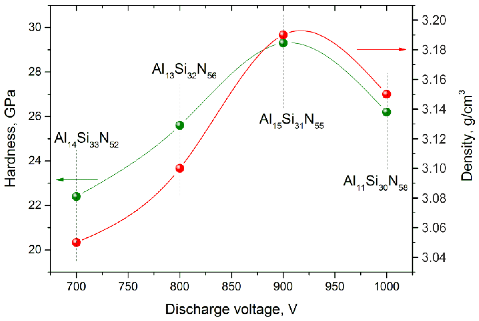
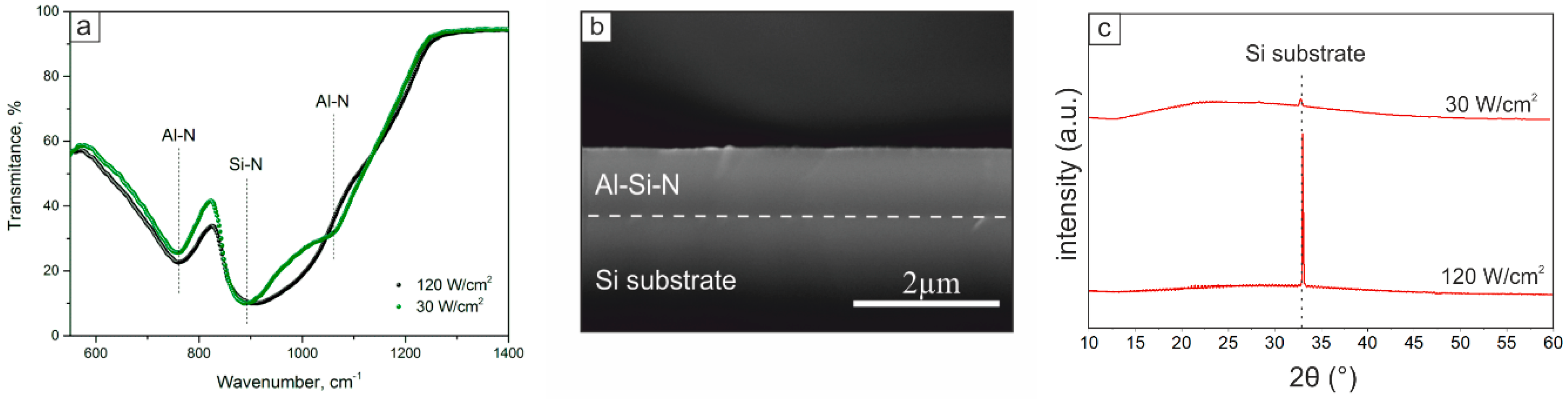
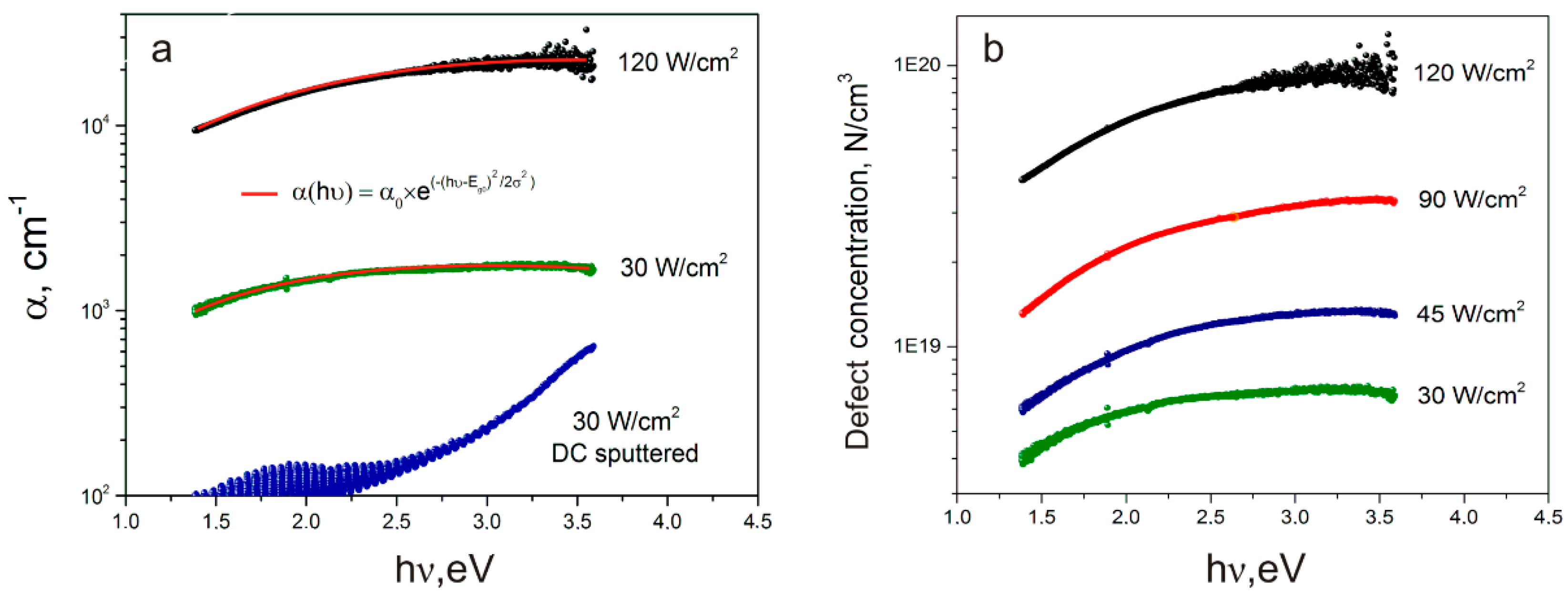
Al–Si–N films were sputtered using a round unbalanced magnetron equipped by an Al/Si (25 at.%/75 at.%) target. The magnetron was powered by the HIPIMS power supply (1 kV, 5 kW, Applied Electronics, Tomsk, Russia). The base pressure p0 in the evacuated deposition chamber was 8 × 10⁻⁴ Pa. We sputtered the Al–Si–N films on Si (100) and glass substrates under the following deposition conditions: discharge voltage Ud = 700–1000 V, pulse period τ = 10 µs, pulse frequency f = 2 kHz, substrate temperature Ts = 300 °C, substrate-to-target distance ds-t = 100 mm, argon flow ϕAr = 100 sccm, nitrogen flow ϕN = 100 sccm, argon pressure pAr = 0.133 Pa, and nitrogen pressure pN = 0.5 Pa. The sputtering system allows us to control the magnetron sputtering voltage in the range of Ud = 700–1000 V with the corresponding discharge current Id = 150–350 A. The average target power density ws was calculated as:
w s = 1 T 0 T U d ( t ) I d ( t ) d t S
here, T is the pulse period, S is the target area ≈80 cm2.
Resulting average target power density ws was in the range of 30–120 W/cm2 for Us = 700–1000 V respectively. This strong sputtering power leads to a high ionization degree of the sputtering material [13]. In order to estimate the plasma ionization level at the various target power densities, we used a plasma optical emission spectroscopy (AvaSpec-ULS2048XL-EVO, Avantes, Apeldoorn, The Netherlands) and selected the characteristic lines of aluminum (Al+ (510 nm), Al++ (607 nm)), silicon (Si+ (615 nm), Si++ (578 nm)) and nitrogen (N+ (746 nm)). The coating’s cross-sectional morphology and elemental composition were studied using a scanning electron microscope equipped with an EDS detector (Quanta SEM, FEI, Hillsboro, OR, USA). Structural characteristics of the coatings were studied using X-ray diffraction (Shimadzu XRD 6000, Shimadzu, Kyoto, Japan) in the Bragg–Brentano configuration with Cu Kα (λ = 0.154 nm) radiation. Infrared spectra of the sputtered films were measured by the FTIR spectrometer (Nicolet 5700, Thermo Electron Corporation, Waltham, MA, USA). The density of the sputtered films was measured by the film mass divided by volume, where the film mass is calculated by the difference of the substrate-film system masses before and after the film deposition, and the volume is calculated by the multiplication of the film thickness and the area of the Si substrate.

3. Results

Figure 1a shows the experimental current-voltage diagram of the HiPIMS for ws = 120 W/cm2. The resulted peak current Id = 350 A with the attributed discharge voltage Ud = 1000 V gives a peak discharge power density up to 4.5 kW/cm2. Figure 1b shows the selected line intensities of the OES spectra for the target material atoms (Al and Si) and nitrogen atoms at the various discharge voltages and the corresponding average target power density.
Line intensities exponentially increase with the increasing of the discharge voltage, especially for ionized atoms at the higher ion charge states (Al++ and Si++) with the change of a discharge voltage from 700 to 1000 V with the corresponding target power density change from 30 up to 120 W/cm2. At the substrate floating potential Uf ≈ −25 V that gives a strong ion bombardment of the growing film with the ion energies up to 80 eV (up to 30 eV of the ion initial energy [18]) and densification of the growing film, as shown in Figure 2. The density of the sputtered Al–Si–N films is correlated with their stoichiometry. The maximum density of the sputtered film deposited at Ud = 900 V is related to the Al11Si31N55 composition, giving the stoichiometry AlN/Si3N4. A higher increase of the discharge voltage leads to the intense bombardment by the high energy N+ ions and enlarged nitrogen concentration in the growing film. For the film deposited at Ud = 1000 V, a resulted film composition Al11Si30N58 gives an overstochiometric nitrogen concentration. Values of hardness of the sputtered films is also strongly correlated with the elemental composition. The maximum value of H = 29.3 GPa is attributed to fully stoichiometric AlN/Si3N4, while the change of the stoichiometry leads to the decreasing of the Al–Si–N film hardness, as shown in Figure 2.
In order to characterize the structure of the sputtered films, we use FTIR measurements, X-ray diffraction and SEM measurements, as shown in Figure 3. Al–Si–N film prepared at ws = 30 W/cm2 exhibits a fully amorphous structure in agreement with previously reported studies [5], as shown in Figure 3b. Additionally, Al–Si–N films are show the same cross-sectional morphology for all target power densities.
No lines of AlN or Si3N4 also cannot be detected on the XRD measurements, as shown in Figure 3c. FTIR spectra of the same film consists of two peaks attributed to the Al–N stretching (780 and 1050 cm−1) and one strong peak of the Si–N stretching (~900 cm−1), as shown in Figure 3a. While an increase of the sputtering power up to 120 W/cm2 did not change the XRD pattern of Al–Si–N, on the FTIR spectra, one can detect a broadening of the Si–N peak at ~900 cm−1 possibly due to the nitrogen dissolving.
A strong ion bombardment during the HiPIMS sputtering process leads to the high concentration of light absorption centers in the film. We found the correlation of light absorption center’s concentration and deposition parameters by the measurement of optical absorption properties of the sputtered Al–Si–N films on the silica glass substrate. The spectral dependence of the absorption coefficient was calculated as:
α ( h ν ) = D ( h ν ) / d
here, D() is a spectral characteristic of the optical density and d is the film thickness. The thickness of all studied Al–Si–N films was 1 ± 0.1 μm.
We estimated the absorption center’s concentration by the Smacula–Dexter formula:
N = 0.87 × 10 17 × n ( n + 2 ) 2 × γ f × α 0
here, n is the materials refractive index, f is the oscillator order (in our case f is assumed as 1), α 0 is the absorption coefficient at the maximum of the local line with the center at 0 and half width γ.
In comparison with the Al–Si–N films previously sputtered by the DC and pulsed magnetron sputtering [19], the HiPIMS sputtered Al–Si–N films show absence of “monoenergetic” optical absorption centers, which are attributed to point defects, as shown in Figure 4. The absorption center’s concentration for the HiPIMS sputtered film is an order of magnitude higher in comparison with the DC sputtered thin film at the same target power density ws = 30 W/cm2 due to enlarged penetration of nitrogen ions during the sputtering process, as shown in Figure 4a.
We analyzed the spectral characteristics of the sputtered films by the inter-zone absorption model for the amorphous and highly defective materials [20]:
α ( h ν ) = α 0 × e ( h ν E g 0 ) 2 / 2 σ 2
Here, α 0 is a constant, Eg0 is the median value of the materials band gap, and σ′2 is the dispersion of Eg, characterized by the defect disorder.
Due to the good approximation of the experimental data by Equation (4), one can conclude that sputtered material consists of nanocrystals of Al–Si–N embedded into the amorphous Si3N4 matrix, which is in agreement with FTIR and XRD data, as discussed above. The synthesized films show a direct band gap Eg0 = 2.98–3.44 eV with the dispersion σ′ = 1.38–1.53, as can be seen in Table 1. The absorption coefficient and the corresponding absorption center’s concentration increases with the increasing of an average magnetron target power density, as shown in Figure 4b, from 1018/cm3 for ws = 30 W/cm2 up to 1020/cm3 for ws = 120 W/cm2. At the same time, the values of the median band gap and the optical gap increase with the correlated decreasing of the Urbach energy and the band gap dispersion of the film material, as shown in Table 1. Median band gap increases from 2.98 eV, which is a close value to the band gap of the fully amorphous silicon nitride [21] to the 3.44 eV, which is in correlation with increasing of the target power density possibly due to the formation of nanocrystalline Si3N4 and AlN (band gaps 5.1 and 6.2 eV respectively). Based on these data, one can conclude the reduction of the disorder in the growing material with the increasing of the magnetron target power density by the defects clustering.

4. Conclusions

In conclusion, we show that mechanical and optical characteristics of the silicon-rich Al–Si–N films are heavily dependent on the sputtering voltage and power density of the HiPIMS discharge. The optimum value of sputtering power is around ws = 90W/cm2, and this gives the optimum stoichiometry AlN/Si3N4 and the highest hardness H = 29.3 GPa, while a higher increase of the sputtering power leads to the reduction of the hardness due to the enlarged amount of nitrogen in the growing film. The optical characteristics of the sputtered Al–Si–N films are correlated with the nitrogen concentration in the growing film. The HiPIMS sputtered Al–Si–N films show an absence of “monoenergetic” optical absorption centers, which are attributed to point defects, while the total concentration of the light absorption centers is an order of magnitude higher in comparison with the DC sputtered thin film at the same target power density.

Author Contributions

Methodology, S.Z.; Validation, S.Z. and F.K.; Formal Analysis, S.Z., A.L. and F.K.; Investigation D.Z. and S.D.; Writing—Original Draft Preparation, S.Z. and F.K.; Writing—Review and Editing, S.Z., A.L., S.D. and D.Z.

Funding

The research was funded by the Tomsk Polytechnic University within the framework of Tomsk Polytechnic University Competitiveness Enhancement Program grant.

Conflicts of Interest

The authors declare no conflict of interest.

References

  1. Yang, M.; Wang, H.; Ma, X.; Gao, H.; Wang, B. Effect of nitrogen-accommodation ability of electrodes in SiNx-based resistive switching devices. Appl. Phys. Lett. 2017, 111, 233510. [Google Scholar] [CrossRef]
  2. Guo, H.; Herkommer, C.; Billat, A.; Grassani, D.; Zhang, C.; Pfeiffer, M.H.P.; Weng, W.; Brès, C.; Kippenberg, T.J. Mid-infrared frequency comb via coherent dispersive wave generation in silicon nitride nanophotonic waveguides. Nat. Photonics 2018, 12, 330–335. [Google Scholar] [CrossRef] [Green Version]
  3. Souza, J.V.C.; Nono, M.C.A.; Ribeiro, M.V.; Machado, J.P.B.; Silva, O.M.M. Cutting forces in turning of gray cast iron using silicon nitride based cutting tool. Mater. Des. 2009, 30, 2715–2720. [Google Scholar] [CrossRef]
  4. Negro, L.D.; Yi, J.H.; Michel, J.; Kimerling, L.C.; Chang, T.-W.F.; Sukhovatkin, V.; Sargent, E.H. Light emission efficiency and dynamics in silicon-rich silicon nitride films. Appl. Phys. Lett. 2006, 88, 233109. [Google Scholar] [CrossRef] [Green Version]
  5. Musil, J.; Javdošňák, D.; Čerstvý, R.; Haviar, S.; Remnev, G.; Uglov, V. Effect of energy on the formation of flexible hard Al-Si-N films prepared by magnetron sputtering. Vacuum 2016, 133, 43–45. [Google Scholar] [CrossRef]
  6. Shen, Z.; Zhao, Z.; Peng, H.; Nygren, M. Formation of tough interlocking microstructures in silicon nitride ceramics by dynamic ripening. Nature 2002, 417, 266–269. [Google Scholar] [CrossRef] [PubMed]
  7. Nishiyama, N.; Ishikawa, R.; Ohfuji, H.; Marquardt, H.; Kurnosov, A.; Taniguchi, T.; Kim, B.; Yoshida, H.; Masuno, A.; Bednarcik, J.; et al. Transparent polycrystalline cubic silicon nitride. Sci. Rep. 2017, 7, 44755. [Google Scholar] [CrossRef] [Green Version]
  8. Musil, J.; Remnev, G.; Legostaev, V.; Uglov, V.; Lebedynskiy, A.; Lauk, A.; Procházka, J.; Haviar, S.; Smolyanskiy, E. Flexible hard Al–Si–N films for high temperature operation. Surf. Coat. Technol. 2016, 307, 1112–1118. [Google Scholar] [CrossRef]
  9. Sergeev, V.; Psakhie, S.; Chubik, P.; Cherniavsky, A.; Soloviev, V.; Solntsev, V.; Khristenko, Y. Magnetron sputtering of Si–Al–N nanocomposite coatings on quartz for protection against impacts of high speed microparticles. Vacuum 2017, 143, 454–457. [Google Scholar] [CrossRef]
  10. Pélisson, A.; Parlinska-Wojtan, M.; Hug, H.J.; Patscheider, J. Microstructure and mechanical properties of Al–Si–N transparent hard coatings deposited by magnetron sputtering. Surf. Coat. Technol. 2007, 202, 884–889. [Google Scholar] [CrossRef]
  11. Jiang, X.; Yang, F.; Chen, W.; Lee, J.; Chang, C. Effect of nitrogen-argon flow ratio on the microstructural and mechanical properties of AlSiN thin films prepared by high power impulse magnetron sputtering. Surf. Coat. Technol. 2017, 320, 138–145. [Google Scholar] [CrossRef]
  12. Ding, J.C.; Wang, Q.M.; Liu, Z.R.; Jeong, S.; Zhang, T.F.; Kim, K.H. Influence of bias voltage on the microstructure, mechanical and corrosion properties of AlSiN films deposited by HiPIMS technique. J. Alloy. Compd. 2019, 772, 112–121. [Google Scholar] [CrossRef]
  13. Anders, A. Tutorial: Reactive high power impulse magnetron sputtering (R-HiPIMS). J. Appl. Phys. 2017, 121, 171101. [Google Scholar] [CrossRef] [Green Version]
  14. Yang, Y.; Tanaka, K.; Liu, J.; Anders, A. Ion energies in high power impulse magnetron sputtering with and without localized ionization zones. Appl. Phys. Lett. 2015, 106, 124102. [Google Scholar] [CrossRef] [Green Version]
  15. Belosludtsev, A.; Houška, J.; Vlček, J.; Haviar, S.; Čerstvý, R.; Rezek, J.; Kettner, M. Structure and properties of Hf–O–N films prepared by high-rate reactive HiPIMS with smoothly controlled composition. Ceram. Int. 2017, 43, 5661–5667. [Google Scholar] [CrossRef]
  16. Cemin, F.; Abadias, G.; Minea, T.; Furgeau, C.; Brisset, F.; Solas, D.; Lundin, D. Benefits of energetic ion bombardment for tailoring stress and microstructural evolution during growth of Cu thin films. Acta Mater. 2017, 141, 120–130. [Google Scholar] [CrossRef]
  17. Pélisson-Schecker, A.; Hug, H.J.; Patscheider, J. Morphology, microstructure evolution and optical properties of Al–Si–N nanocomposite coatings. Surf. Coat. Technol. 2014, 257, 114–120. [Google Scholar] [CrossRef]
  18. Jouan, P.; le Brizoual, L.; Ganciu, M.; Cardinaud, C.; Tricot, S.; Djouadi, M. HiPIMS ion energy distribution measurements in reactive mode. IEEE Trans. Plasma Sci. 2010, 38, 3089–3094. [Google Scholar] [CrossRef]
  19. Kabyshev, A.V.; Konusov, F.V.; Lauk, A.L.; Lebedynskiy, A.M.; Legostaev, V.N.; Smolyanskiy, E.A. Optical absorption peculiarities of Al-Si-N coatings produced by magnetron sputtering. Key Eng. Mater. 2016, 712, 3–8. [Google Scholar] [CrossRef]
  20. Konusov, F.V.; Kabyshev, A.V.; Remnev, G.E. Optical properties of GaAs films deposited via pulsed ion ablation. J. Surf. Invest. 2011, 5, 228–235. [Google Scholar] [CrossRef]
  21. Wang, Q.; Ward, S.; Gedvilas, L.; Keyes, B.; Sanchez, E.; Wang, S. Conformal thin-film silicon nitride deposited by hot-wire chemical vapor deposition. Appl. Phys. Lett. 2004, 84, 338–340. [Google Scholar] [CrossRef]
Figure 1. Single pulse characteristics (a) and optical emission spectroscopy intensities of selected lines (b) of HiPIMS discharge.
Coatings 09 00053 g001
Figure 2. Hardness, density and elemental composition of sputtered Al–Si–N films that are dependent on the HiPIMS discharge voltage.
Coatings 09 00053 g002
Figure 3. (a) FTIR spectra of Al–Si–N films prepared at ws = 30 W/cm2 (green) and 120 W/cm2 (black); (b) SEM image of the Al–Si–N film prepared at ws = 30 W/cm2; (c) Diffraction patterns of Al–Si–N films prepared at 30 W/cm2 HiPIMS discharge power (top) and Al–Si–N films prepared at 120 W/cm2 HiPIMS discharge power (bottom).
Coatings 09 00053 g003
Figure 4. (a) Spectral dependence of the absorption coefficient; (b) absorption center’s concentration in dependence with the average HiPIMS discharge power density.
Coatings 09 00053 g004
Table 1. Optical characteristics of the sputtered Al–Si–N films in dependence with the HiPIMS target power density.
Target Power Density w (W/cm2)Film Band Gap Eg0 (eV)Band Gap Dispersion σ′ (eV)Urbach Energy EU (eV)Optical Gap Eg′ (eV)
302.981.531.861.6
453.141.401.481.8
903.221.381.332.01
1203.441.51.152.04

