Communication

Ordered Array of Metal Particles on Semishell Separated with Ultrathin Oxide: Fabrication and SERS Properties

1
School of Materials Science and Engineering, Nanyang Technological University, Singapore 639798, Singapore
2
College of Education Science, Hunan First Normal University, No.1015, Fenglin Road (the 3rd), Yuelu District, Changsha 410205, China
3
Division of Physics and Applied Physics, School of Physical and Mathematical Sciences, Nanyang Technological University, Singapore 637371, Singapore
*
Author to whom correspondence should be addressed.
Coatings 2019, 9(1), 20; https://doi.org/10.3390/coatings9010020
Submission received: 22 October 2018 / Revised: 14 December 2018 / Accepted: 14 December 2018 / Published: 29 December 2018
(This article belongs to the Collection Advanced Surface Coating of Nanoparticles)

Abstract

:
Metal particles in gap cavities provide an interesting system to achieve hybrid local surface plasmon modes for local field enhancement. Here, we demonstrate a relatively simple method to fabricate Ag nanoparticles positioned on Ag semishells separated by a thin (~5 nm) dielectric layer. The obtained structure can provide strong local electric field enhancement for surface-enhanced Raman scattering (SERS). The fabrication of the ordered array structure was realized by nanosphere self-assembly, atomic layer deposition, and metal thin-film dewetting. Numerical simulation proved that, compared to the conventional metal semishell arrays, the additional Ag particles introduce extra hot spots particularly in the valley regions between adjacent Ag semishells. As a result, the SERS enhancement factor of the metal semishell-based plasmonic structure could be further improved by an order of magnitude. The developed novel plasmonic structure also shows good potential for application in plasmon-enhanced solar water-splitting devices.

1. Introduction

As a powerful spectroscopic technique, surface-enhanced Raman scattering (SERS) has found increased applications in various fields, including analytical chemistry, life sciences, medical sciences, and food safety [1,2,3,4,5,6,7,8,9]. One major challenge in making SERS a general analytical tool lies in the fabrication of noble metal nanostructure substrates with large and reproducible Raman enhancements over a wide sampling area, using ideally less costly, high-throughput methods [4,10,11,12,13,14,15,16]. Among various nanofabrication techniques for SERS substrates, nanosphere monolayer self-assembly (alternatively referred to as nanosphere lithography) has been widely adopted as a facile, inexpensive, and reliable fabrication method for the production of large-area ordered nanostructures [17,18,19,20,21,22,23,24,25,26]. In particular, metal semishell array substrates have been widely employed in many SERS-based biosensing applications in complex media [27,28]. These semishell array substrates consist of ordered nanogaps between the spheres, which create plasmonic features with good control and tunability compared to random metal structures [29]. Nevertheless, the SERS enhancement factors of these semishell array substrates in previous studies were only around 104–105 [29]. This is because in most of these conventional metal array nanostructures, there are only limited number of plasmonic ‘hot spots’ contributing to the overall SERS signal, and the metal gap size is still generally very large compared to the desirable sub-10 nm regime [29,30,31]. It is therefore desirable to further increase the SERS enhancement through increasing the density of hot spots within the same sample surfaces and/or the local field by engineering the nanostructures.
Based on the well-established nanosphere monolayer assembly, more sophisticated structures have been fabricated in order to increase the enhancement factor, such as structures with particles in cavities [32]. For example, Im et al. found that the SERS of an Ag semishell array can be further improved by an order of magnitude by constructing a nanoring cavity on top, forming sub-10 nm nanogaps [33]. In addition, the particle-in-cavity structures, such as particle-in-void and particle-in-bowl, have been also demonstrated to produce noticeably high-field enhancement in the nanogaps between the metal particles and the metal surface [34,35]. Overall, a further increase of SERS enhancement factors relies essentially on the formation of sub-10 nm plasmonic nanogaps [12]. To meet this challenge, atomic layer deposition (ALD) has shown to be capable of conformal and uniform coating of thin films of atomic thickness on 3D surfaces and has been widely employed in nanofabrication and surface engineering of photonics and energy-conversion materials, such as the ALD-fabricated 3D inverse opal structure photoanodes for photoelectron chemical water splitting [36,37]. Recently, ALD has also been proven useful in the fabrication of novel plasmonic structures, for example, an ultrathin isolated dielectric layer on Au particles for ultra-sensitive SERS [38] and nanogaps in plasmonic structures [39,40].
In this communication, we demonstrate a facile and scalable fabrication process based on nanosphere monolayer assembly and atomic layer deposition to achieve an array structure with metal particles on semishell (PoSS) for SERS application. The metal particles were formed via a simple thermal-induced dewetting of thin film. The local field enhancement of the PoSS structure was verified by both simulation and SERS measurements. This subtle design of the PoSS array generated further SERS enhancement up to 10 times that of conventional metal semishell arrays (although still not higher than those of other SERS structures obtained by less scalable or less reproducible fabrication methods). Our results demonstrate the usefulness of nanosphere self-assembly and ALD in fabricating plasmonic nanostructures for applications in biomedical sciences and surface plasmon-enhanced solar water-splitting devices.

2. Materials and Methods

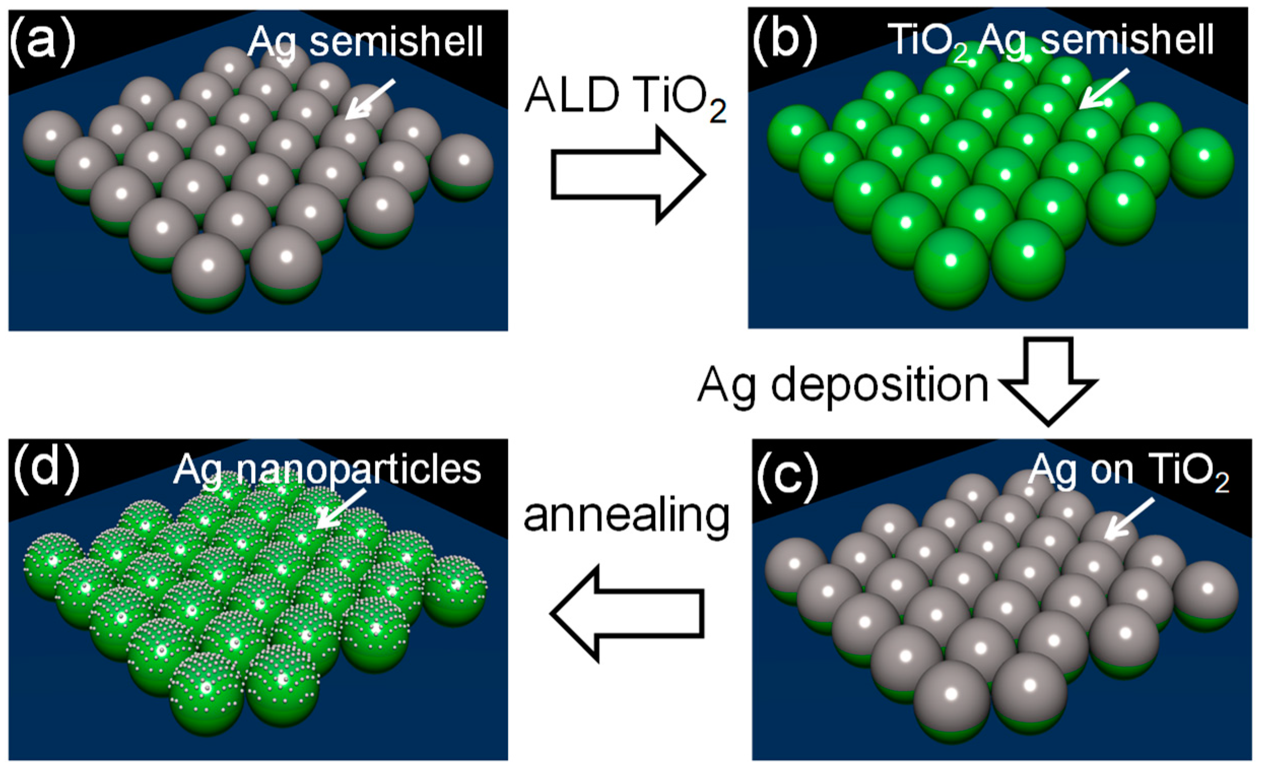
2.1. Fabrication of the Metal Semishell (PoSS) Array

The fabrication process for the PoSS array is illustrated in Figure 1. First, a ~100 nm-thick Ag layer was deposited on the hollow TiO2 array by an Edward electron-beam evaporation system, as shown in Figure 1a. The fabrication process of the hollow TiO2 nanosphere array has been reported elsewhere [31], and its steps include self-assembly of monolayer polystyrene (PS) spheres, reactive ion etching, ALD TiO2, and thermal annealing (450 °C for one hour). PS nanospheres were purchased from Polysciences, Inc., Warrington, FL, USA. The concentration of the PS used in this study was 2.61% (w/w), and the size distribution of the PS was 505 ± 10 nm. After Ag deposition, a 5 nm TiO2 layer was coated on the Ag films using ALD, as shown in Figure 1b,c. ALD was performed on a Beneq TFS-200 system (Espoo, Finland) using TiCl4 and deionized water as Ti and oxygen precursors, respectively. High-purity N2 was used as the process gas in our experiment. During the deposition, the reaction chamber was maintained at 1.0 mbar with a steady N2 steam at 200 sccm. Each ALD cycle consisted of a 250 ms precursor pulse and 5 s purging time with N2, and 60 cycles were used to deposit a 5 nm-thick TiO2. The deposition temperature was set to a low temperature of 60 °C for two reasons: to avoid oxidation of the Ag film and to simultaneously reduce the crystallization and conductivity of the TiO2 layer. Finally, a thin Ag layer of variable thickness was sputtered (JFC-1600, JEOL, Tokyo, Japan) followed by thermal annealing at 120 °C in an Ar atmosphere for 30 min. The final heating process converted the top Ag thin film to individual particles via dewetting, as shown in Figure 1d. The coverage of Ag particles was controlled by the sputtering time at a fixed current of 10 mA.

2.2. Characterization
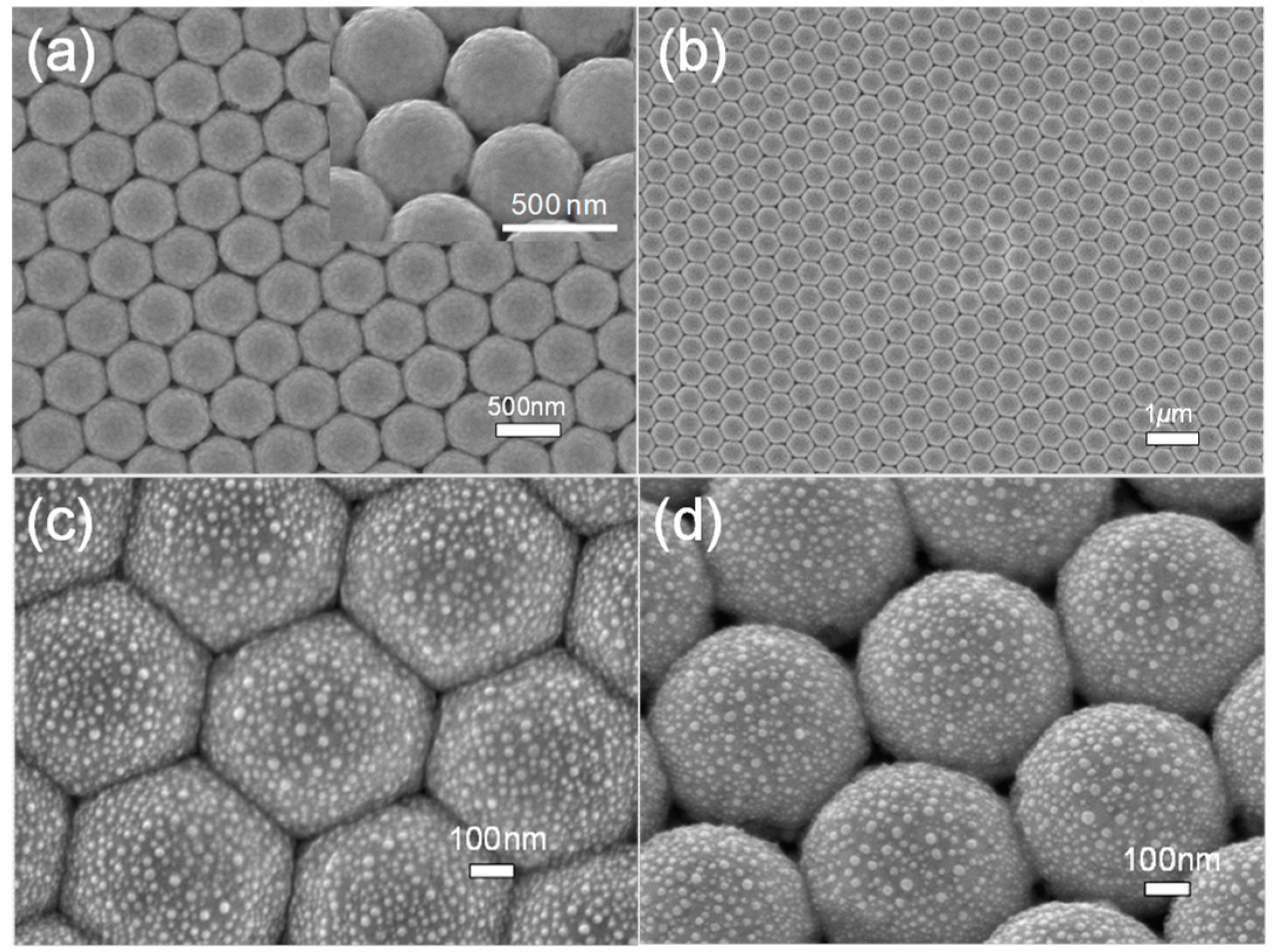
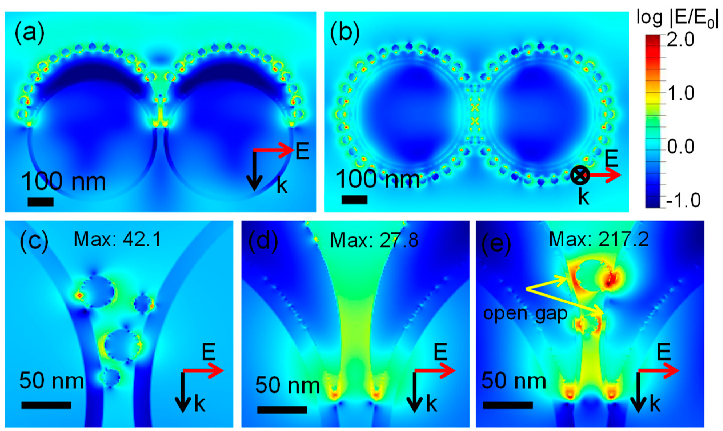
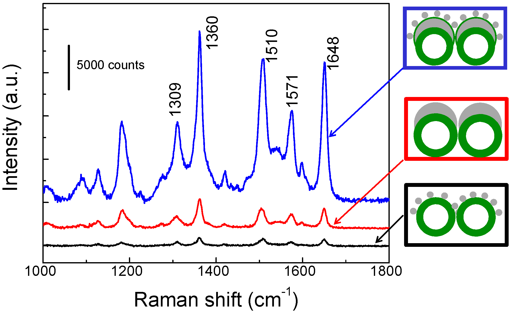
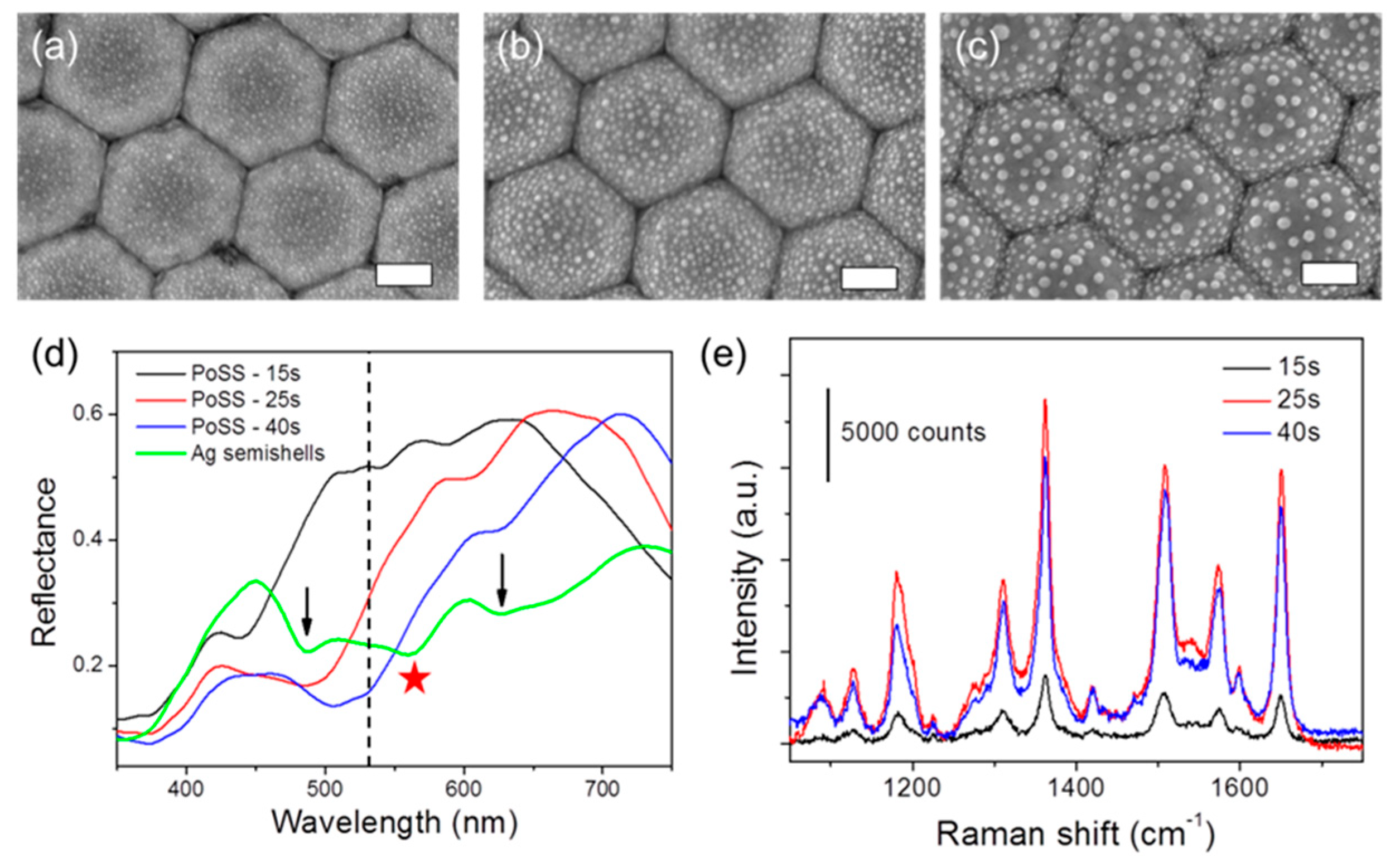
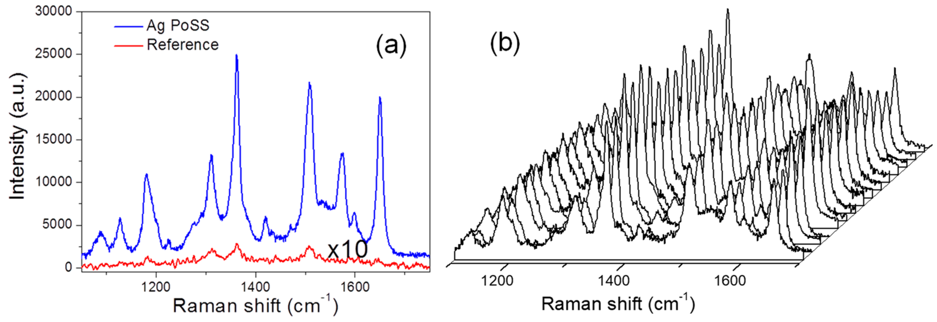
The morphology of the PoSS array was characterized by JEOL JSM-6700F field emission scanning electron microscope (FE-SEM). Diffused reflectance spectra were recorded by a Zolix Solar Cell QE/IPCE measurement system (Zolix Instruments Co., Ltd., Beijing, China) equipped with an integrated sphere and a Si diode. To avoid oxidation of Ag, fresh samples were used for SERS measurements.
For SERS measurements, R6G was utilized as the standard probe molecule. The substrates were immersed in the prepared R6G solution at the concentration of 0.5 μM for 30 min, then washed with deionized water, and dried by N2 flow before SERS measurements. The Raman spectra were recorded using a Renishaw Raman Imaging Microscope (Wotton-under-Edge, UK) configured with a charge-coupled device (CCD) array detector and a 50× short focal length objective. A 532 nm laser with the output power of 25 mW was used. The incident power on the sample surface was reduced to 1% of the output. The laser focal spot on the sample surface was ~1 μm in diameter, and the focus depth was ~20 μm. The SERS spectra were collected in the wave number range of 1000–2000 cm−1 with fixed acquisition time of 10 s. Each spectrum shown in this paper is the average of five spectra measured from different locations on the same sample surface.

3. Results

Since ALD is a cyclic layer-by-layer deposition method, it is capable of conformal and uniform coating of thin films on 3D surfaces. In our study, the ALD TiO2 layer covered the whole surface of the Ag semishell array structure with a controllable thickness down to a few nanometers. The TiO2 layer has two functions: firstly, it serves as a dielectric separation layer of the Ag particles from the Ag film; secondly, it protects the Ag semishells from distortion during the final thermal annealing process. The size of the coated particles can be tuned by the sputtering time, which will be further discussed later. While the metal demonstrated herein used Ag, the fabrication and main conclusion are essentially the same for gold.
Figure 2a shows a scanning electron microscope (SEM) image of the fabricated hexagonal close-packed Ag semishell array with PS size of (505 ± 10) nm. The final Ag PoSS structures are shown in Figure 2b–d. The Ag semishells underneath were well maintained during the thermal annealing process at 120 °C, otherwise discontinuous islands would have been observed. The size of the particles located in the valley region between adjacent spheres should be slightly smaller than that of the ones located at the top, due to the fact the Ag film deposited laterally on the spheres’ surface could be thinner than that deposited on top, as a consequence of the so-called shadowing effect.
Firstly, a numerical estimation of the electromagnetic field distribution in the PoSS structure was carried out using a 3D finite-difference time-domain (FDTD) simulation (FDTD Solution 8.5, Lumerical Inc., Vancouver, BC, Canada). For simplicity, the Ag particles were treated as spheres. The outer diameter of the TiO2 hollow spheres in the simulations was 490 nm, and the shell thickness was 15 nm. The distance of the two TiO2 hollow spheres was set to 505 nm. The ALD TiO2 layer between the Ag particle and Ag semishell was set to 5 nm. The Ag particle size was chosen to be 30 nm, and for close-view simulation, we set two different particles with diameters of 30 and 16 nm. Because of the size distribution and the random location of the Ag nanoparticles on the semishell, the periodic boundary condition of the original Ag semishell array was broken. Moreover, as the Ag particle size (30–16 nm) was relatively small compared to the semishells (~500 nm), the PoSS structure could be treated as the well-known ‘metal-particle-on-metal-film’ system [41]. Thus, a dimer structure was chosen as the unit structure in the simulation. The Yee cell in our calculation was set to 1.0 nm × 1.0 nm × 1.0 nm [35]. These settings are sufficient for characterizing the features of the given geometry. The dielectric constant of Ag was obtained from Johnson and Christy [42], and that for TiO2 from Palik (‘Handbook of Optical Constants of Solids’). The particle in a uniform dielectric medium (n = 1) was illuminated from the top with a 532 nm linear polarized plane wave, as shown in Figure 3a. Figure 3a,b shows the simulation result of the structure from the side view and top view, respectively. The simulation results show that the PoSS structure generated localized hybrid surface plasmons and substantial electromagnetic field enhancement between the Ag particles and the Ag film. These gaps are known as plasmonic hot spots for SERS, provided that they are accessible by analytic molecules. For the commonly studied metal semishells, however, the hot spots are located merely at the edge of the shells between adjacent spheres (see Figure 3d). After particle coating, each Ag particle generated one more hot spot. This means the density of hot spots significantly increased in the PoSS array structure. Another important feature of the PoSS structure is the drastic field enhancement in the valley region. Let us take a closer inspection and compare it to control structures of pure Ag particles without an Ag film underneath as well as to pure Ag semishells. As seen in Figure 3c–e, because of the strong coupling between Ag particles and Ag semishells, the addition of Ag particles, produced new electric fields stronger than those produced by the bare Ag semishell array and Ag particles directly on TiO2 spheres. Although the largest field enhancement was found to be at the touching area between the Ag particles and the TiO2 interlayer (Figure 3e), the non-touching side (indicated with yellow arrows), which had a molecule-accessible surface, also exhibited strong fields. It is believed that these open hot spots contributed dominantly to the SERS, as other hot spots beneath the touching points were not accessible to analytic molecules.
The overall field enhancement could be characterized by SERS measurements. Figure 4 shows the Raman spectra collected from Ag PoSS arrays obtained from 25 s Ag deposition (blue curve) and those from the bare Ag semishell array (red line) and the Ag particles on TiO2 spheres without Ag semishells (black line) for comparison. One can see that the Raman signal from the Ag PoSS array showed the strongest SERS signal, which was nearly 10 times that from the bare Ag semishell array. For the Ag particles coated on TiO2 hollow spheres, the signal intensity was rather low. This can be explained by the small local field enhancement in the structure, as revealed by simulation in Figure 3c. In addition, the relatively large separation between individual Ag particles (as shown in SEM images) made the coupling between localized surface plasmon (LSP) modes of the particles negligible.
The Ag nanoparticle size and the SERS enhancement of the PoSS array could be tuned by modulating the Ag sputtering time. Figure 5 shows the SEM images of the Ag PoSS structure fabricated using different Ag sputtering times. When the sputtering time increased from 15 to 40 s, the Ag particle size increased from ~8 to 30 nm. Diffuse reflection spectra of the samples with different Ag deposition times are shown in Figure 5d. For comparison, the spectrum from the bare Ag semishells on TiO2 hollow sphere arrays is also shown. The absorption edge at 380 nm observed for all samples corresponds to the bulk value (3.2 eV) of the TiO2 band gap. The Ag semishell array substrate exhibited two broad localized surface plasmon resonance (LSPR) peaks, located at ~480 and ~630 nm, which correspond to the axial and transverse modes of the Ag semishell, respectively. This result is consistent with previous reports on the Ag semishell array [29,33]. The minimum reflectance at ~560 nm (indicated by the red star) is due to the hexagonal close-packed structure [31]. The reflection spectrum of the final PoSS structure with 40 s sputtering time showed two plasmon bands at ~520 and ~620 nm, indicated with black arrows in Figure 5d. These two peaks could be due to the plasmon coupling between the particle and the semishell. As the Ag particle size (50 nm) is relatively small compared to the semishells (~500 nm), the PoSS structure can be regarded as the well-known ‘metal-particle-on-metal-film’ system. In such a particle-on-film system, it is known that there exist two plasmon modes, the horizontal and the vertical modes, as previously described [43,44]. The vertical mode has lower resonance energy than the horizontal mode. The s- and p-polarized incident lights excite the horizontal and vertical modes, respectively [43]. In our case, as the Ag particles were anchored on a curved semishell surface, both horizontal and vertical modes could be excited under a normal incident condition. With a decrease in the Ag sputtering time, the corresponding plasmon peaks blueshifted because of the reduction of Ag particle size (as seen in Figure 5a–c). Moreover, because the Ag PoSS structure was fabricated on the basis of a hexagonal close-packed PS monolayer template, it had a 60° rotational symmetry. Thus, the polarization effect would be only within 30° as a result of the rotational symmetry. Because of these two factors, the polarization effect was greatly weakened in our SERS measurements.
The SERS enhancement was accordingly dependent on the Ag sputtering time. Figure 5e shows that the PoSS structures with 25 and 40 s Ag depositions had similar SERS intensities, both significantly higher than that of the 15 s sample. The simulation results (Figure 3) indicated that the particles in the valley region gave the dominant contribution to the SERS enhancement. Therefore, the difference in their SERS intensity in Figure 5e should be related to the numbers of Ag particles in the valley region. The size of the particles as well as the LSPR resonance frequency affect the strength of the local field. For the three PoSS structures, it is hypothesized that the drastically low Raman intensity of the 15 s sample originated from the blueshift of the LSPR wavelength away from the excitation wavelength (532 nm), as seen in Figure 5d. The slight difference between the 25 and 40 s sample can be ascribed to a tradeoff between particle size and number of open hot spots within the valley region.
Finally, we estimated the SERS enhancement factor (EF). EF characterizes the sensitivity of a SERS substrate, which is defined by the ratio of the intensity of the SERS signal to that of the normal Raman signal (i.e., not surface-enhanced) or the non-SERS signal [45].
EF = (ISERS/NSERS)/(I0/N0)
where N0 and NSERS are the number of probe molecules that contribute to the non-SERS and SERS signals, respectively, and I0 and ISERS are the intensities of the selected scattering bands in the non-SERS and SERS spectra, respectively. The detected molecules were assumed to have been distributed uniformly on the substrates. Thus, the number of the detected molecules could be estimated by
N = (NACVsolution/Ssub)Slaser
where NA is the Avogadro constant, C is the molar concentration of the prepared solution, Vsolution is the volume of the solution used, Ssub is the size of the substrate, and Slaser is the size of the laser spot. To prepare the SERS sample, 2 μL of 0.5 μM R6G solution was dropped on the Ag PoSS structure (Ag sputtering time 25 s) substrate, with a drop diameter of approximately 4 mm. For the reference, 2 μL of 10 mM R6G solution was dropped on a single crystal gold foil for the non-SERS measurements, with a drop diameter of approximately 4 mm. Since the samples for SERS and non-SERS detection were prepared by the same method, the EF could be estimated by the following Equation.
EF =(ISERS/CSERS)/(I0/C0)
where CSERS and C0 are the molar concentrations of R6G molecules in the aqueous solutions used for the SERS and non-SERS samples, respectively. A typical comparison of the spectra is shown in Figure 6a. The characteristic band at 1360 cm−1 was chosen for the EF estimation. In this way, the average EF could be as high as ~2.5 × 10⁶ for the PoSS structure (Ag sputtering time 25 s), nearly 10 times that of the bare Ag semishell array (~2.8 × 10⁵). In our previous work on Au semishells, a SERS EF of 1.5 × 10⁵ was also obtained, which was used to detect 10−9 M target solution. [31] Since the EF of Ag PoSS SERS substrate was almost 20 times that of the Au semishell array SERS substrate, the as-fabricated PoSS substrate could potentially be used in the detection of a 10−10 M target molecular solution. It is noted that while this EF is not the highest ever obtained, the main intention of this work was to demonstrate a facile fabrication method of a homogeneous and reproducible SERS structure, for comparison with the solution synthesis of metal nanoparticles or individual nanogaps which can exhibit EFs up to 109. The reproducibility of the SERS signal is another important parameter for the Ag PoSS structure as a SERS substrate. To test the reproducibility of the Ag PoSS SERS substrate, the SERS spectra were collected from 15 randomly selected positions, as shown in Figure 6b. For the peak at 1360 cm−1, the relative standard deviation (RSD) of the SERS intensity was approximately 11.5%. This low RSD indicated that the Ag PoSS SERS substrates had an excellent reproducibility.

4. Conclusions

Assisted by PS sphere self-assembly and ALD, we have demonstrated a controllable fabrication of novel ordered arrays of Ag particles on semishells (PoSS) with a reasonably high SERS effect. The SERS enhancement factor of the PoSS array showed an increase up to 10 times as compared to the commonly studied bare metal semishell arrays. The FDTD simulation revealed that the further SERS enhancement was due to the increase of the local field and the density of plasmonic hot spots in the valley region. The large SERS enhancement of such metal PoSS arrays and their facile, reproducible fabrication process suggest their potential application as functional components in chemical sensors and biosensors. This novel PoSS plasmonic structure can also find application in solar energy conversion, such as plasmon-enhanced solar water-splitting devices.

Author Contributions

Conceptualization, X.L. and A.I.Y.T.; Methodology, Z.W. and C.K.T.; Formal Analysis, X.L.; Simulation, X.L. and Z.S.; Writing—Original Draft Preparation, X.L.; Writing—Review and Editing, Z.W., C.K.T. and A.I.Y.T.; Supervision, A.I.Y.T. and Z.S.; Funding Acquisition, A.I.Y.T.

Funding

This work was supported by Singapore Ministry of Education Academic Research Fund Tier2 Academic Research Fund (No. MOE2014-T2-2-082).

Acknowledgments

The authors would like to thank Hongjin Fan for his valuable comments and suggestions to improve the quality of the paper.

Conflicts of Interest

The authors declare no conflict of interest.

References

  1. Yuan, Y.; Panwar, N.; Yap, S.H.K.; Wu, Q.; Zeng, S.; Xu, J.; Tjin, S.C.; Song, J.; Qu, J.; Yong, K.-T. SERS-based ultrasensitive sensing platform: An insight into design and practical applications. Coord. Chem. Rev. 2017, 337, 1–33. [Google Scholar] [CrossRef]
  2. Cao, Y.W.C.; Jin, R.C.; Mirkin, C.A. Nanoparticles with Raman spectroscopic fingerprints for DNA and RNA detection. Science 2002, 297, 1536–1540. [Google Scholar] [CrossRef] [PubMed]
  3. Demirel, G.; Usta, H.; Yilmaz, M.; Celik, M.; Alidagi, H.A.; Buyukserin, F. Surface-enhanced Raman spectroscopy (SERS): An adventure from plasmonic metals to organic semiconductors as SERS platforms. J. Mater. Chem. C 2018, 6, 5314–5335. [Google Scholar] [CrossRef]
  4. Wang, Z.; Zong, S.; Wu, L.; Zhu, D.; Cui, Y. SERS-activated platforms for immunoassay: Probes, encoding methods, and applications. Chem. Rev. 2017, 117, 7910–7963. [Google Scholar] [CrossRef]
  5. Graham, D.; Thompson, D.G.; Smith, W.E.; Faulds, K. Control of enhanced Raman scattering using a DNA-based assembly process of dye-coded nanoparticles. Nat. Nanotechnol. 2008, 3, 548–551. [Google Scholar] [CrossRef]
  6. Anker, J.N.; Hall, W.P.; Lyandres, O.; Shah, N.C.; Zhao, J.; Van Duyne, R.P. Biosensing with plasmonic nanosensors. Nat. Mater. 2008, 7, 442–453. [Google Scholar] [CrossRef]
  7. van Lierop, D.; Faulds, K.; Graham, D. Separation free DNA detection using surface enhanced Raman scattering. Anal. Chem. 2011, 83, 5817–5821. [Google Scholar] [CrossRef] [PubMed]
  8. Graham, D.; Goodacre, R. Chemical and bioanalytical applications of surface enhanced Raman scattering spectroscopy. Chem. Soc. Rev. 2008, 37, 883–884. [Google Scholar] [CrossRef]
  9. Wang, X.; Shi, W.; Jin, Z.; Huang, W.; Lin, J.; Ma, G.; Li, S.; Guo, L. Remarkable SERS activity observed from amorphous ZnO nanocages. Angew. Chem. Int. Ed. 2017, 56, 9851–9855. [Google Scholar] [CrossRef]
  10. Li, W.Y.; Camargo, P.H.C.; Lu, X.M.; Xia, Y.N. Dimers of silver nanospheres: Facile synthesis and their use as hot spots for surface-enhanced Raman scattering. Nano Lett. 2009, 9, 485–490. [Google Scholar] [CrossRef] [PubMed]
  11. Zhang, B.H.; Wang, H.S.; Lu, L.H.; Ai, K.L.; Zhang, G.; Cheng, X.L. Large-area silver-coated silicon nanowire arrays for molecular sensing using surface-enhanced Raman spectroscopy. Adv. Funct. Mater. 2008, 18, 2348–2355. [Google Scholar] [CrossRef]
  12. Duan, H.; Hu, H.; Kumar, K.; Shen, Z.; Yang, J.K.W. Direct and Reliable patterning of plasmonic nanostructures with sub-10-nm gaps. ACS Nano 2011, 5, 7593–7600. [Google Scholar] [CrossRef] [PubMed]
  13. Wang, X.; Ma, G.; Li, A.; Yu, J.; Yang, Z.; Lin, J.; Li, A.; Han, X.; Guo, L. Composition-adjustable Ag–Au substitutional alloy microcages enabling tunable plasmon resonance for ultrasensitive SERS. Chem. Sci. 2018, 9, 4009–4015. [Google Scholar] [CrossRef] [PubMed]
  14. Ouyang, L.; Wang, Y.; Zhu, L.; Irudayaraj, J.; Tang, H. Filtration-assisted fabrication of large-area uniform and long-term stable graphene isolated nano-Ag array membrane as surface enhanced Raman scattering substrate. Adv. Mater. Interfaces 2018, 5, 1701221. [Google Scholar] [CrossRef]
  15. Huang, Z.; Meng, G.; Huang, Q.; Yang, Y.; Zhu, C.; Tang, C. Improved SERS performance from Au nanopillar arrays by abridging the pillar tip spacing by Ag sputtering. Adv. Mater. 2010, 22, 4136–4139. [Google Scholar] [CrossRef] [PubMed]
  16. Huang, Z.; Lei, X.; Liu, Y.; Wang, Z.; Wang, X.; Wang, Z.; Mao, Q.; Meng, G. Tapered optical fiber probe assembled with plasmonic nanostructures for surface-enhanced Raman scattering application. ACS Appl. Mater. Interfaces 2015, 7, 17247–17254. [Google Scholar] [CrossRef] [PubMed]
  17. Li, Y.; Duan, G.; Liu, G.; Cai, W. Physical processes-aided periodic micro/nanostructured arrays by colloidal template technique: Fabrication and applications. Chem. Soc. Rev. 2013, 42, 3614–3627. [Google Scholar] [CrossRef]
  18. Haynes, C.L.; Van Duyne, R.P. Nanosphere lithography:  A versatile nanofabrication tool for studies of size-dependent nanoparticle optics. J. Phys. Chem. B 2001, 105, 5599–5611. [Google Scholar] [CrossRef]
  19. Lu, Y.; Liu, G.L.; Kim, J.; Mejia, Y.X.; Lee, L.P. Nanophotonic crescent moon structures with sharp edge for ultrasensitive biomolecular detection by local electromagnetic field enhancement effect. Nano Lett. 2004, 5, 119–124. [Google Scholar] [CrossRef]
  20. Liu, X.; Sun, C.-H.; Linn, N.C.; Jiang, B.; Jiang, P. Wafer-scale surface-enhanced Raman scattering substrates with highly reproducible enhancement. J. Phys. Chem. C 2009, 113, 14804–14811. [Google Scholar] [CrossRef]
  21. Zhang, X.; Young, M.A.; Lyandres, O.; Van Duyne, R.P. Rapid detection of an anthrax biomarker by surface-enhanced Raman spectroscopy. J. Am. Chem. Soc. 2005, 127, 4484–4489. [Google Scholar] [CrossRef] [PubMed]
  22. Oh, Y.-J.; Park, S.-G.; Kang, M.-H.; Choi, J.-H.; Nam, Y.; Jeong, K.-H. Beyond the SERS: Raman enhancement of small molecules using nanofluidic channels with localized surface plasmon resonance. Small 2011, 7, 184–188. [Google Scholar] [CrossRef]
  23. Duan, G.; Lv, F.; Cai, W.; Luo, Y.; Li, Y.; Liu, G. General synthesis of 2D ordered hollow sphere arrays based on nonshadow deposition dominated colloidal lithography. Langmuir 2010, 26, 6295–6302. [Google Scholar] [CrossRef] [PubMed]
  24. Liu, G.; Li, Y.; Duan, G.; Wang, J.; Liang, C.; Cai, W. Tunable surface plasmon resonance and strong SERS performances of Au opening-nanoshell ordered arrays. ACS Appl. Mater. Interfaces 2011, 4, 1–5. [Google Scholar] [CrossRef] [PubMed]
  25. Zhang, H.; Zhou, F.; Liu, M.; Liu, D.; Men, D.; Cai, W.; Duan, G.; Li, Y. Spherical nanoparticle arrays with tunable nanogaps and their hydrophobicity enhanced rapid SERS detection by localized concentration of droplet evaporation. Adv. Mater. Interfaces 2015, 2, 1500031. [Google Scholar] [CrossRef]
  26. Yu, J.; Yang, M.; Zhang, C.; Yang, S.; Sun, Q.; Liu, M.; Peng, Q.; Xu, X.; Man, B.; Lei, F. Capillarity-assistant assembly: A fast preparation of 3D pomegranate-like Ag nanoparticle clusters on CuO nanowires and its applications in SERS. Adv. Mater. Interfaces 2018, 5, 1800672. [Google Scholar] [CrossRef]
  27. Patoka, P.; Giersig, M. Self-assembly of latex particles for the creation of nanostructures with tunable plasmonic properties. J. Mater. Chem. 2011, 21, 16783–16796. [Google Scholar] [CrossRef]
  28. Yang, S.-M.; Jang, S.G.; Choi, D.-G.; Kim, S.; Yu, H.K. Nanomachining by colloidal lithography. Small 2006, 2, 458–475. [Google Scholar] [CrossRef]
  29. Wang, C.X.; Ruan, W.D.; Ji, N.; Ji, W.; Lv, S.; Zhao, C.; Zhao, B. Preparation of nanoscale ag semishell array with tunable interparticle distance and its application in surface-enhanced Raman scattering. J. Phys. Chem. C 2010, 114, 2886–2890. [Google Scholar] [CrossRef]
  30. Fang, Y.; Seong, N.-H.; Dlott, D.D. Measurement of the distribution of site enhancements in surface-enhanced Raman scattering. Science 2008, 321, 388–392. [Google Scholar] [CrossRef]
  31. Li, X.; Hu, H.; Li, D.; Shen, Z.; Xiong, Q.; Li, S.; Fan, H.J. Ordered array of gold semishells on TiO2 spheres: An ultrasensitive and recyclable SERS substrate. ACS Appl. Mater. Interfaces 2012, 4, 2180–2185. [Google Scholar] [CrossRef] [PubMed]
  32. Kravets, V.G.; Zoriniants, G.; Burrows, C.P.; Schedin, F.; Geim, A.K.; Barnes, W.L.; Grigorenko, A.N. Composite Au nanostructures for fluorescence studies in visible light. Nano Lett. 2010, 10, 874–879. [Google Scholar] [CrossRef] [PubMed]
  33. Im, H.; Bantz, K.C.; Lee, S.H.; Johnson, T.W.; Haynes, C.L.; Oh, S.-H. Self-assembled plasmonic nanoring cavity arrays for SERS and LSPR biosensing. Adv. Mater. 2013, 25, 2678–2685. [Google Scholar] [CrossRef] [PubMed]
  34. Huang, F.M.; Wilding, D.; Speed, J.D.; Russell, A.E.; Bartlett, P.N.; Baumberg, J.J. Dressing plasmons in particle-in-cavity architectures. Nano Lett. 2011, 11, 1221–1226. [Google Scholar] [CrossRef] [PubMed]
  35. Li, X.; Zhang, Y.; Shen, Z.X.; Fan, H.J. Highly ordered arrays of particle-in-bowl plasmonic nanostructures for surface-enhanced Raman scattering. Small 2012, 8, 2548–2554. [Google Scholar] [CrossRef] [PubMed]
  36. Liu, M.; Li, X.; Karuturi, S.K.; Tok, A.I.Y.; Fan, H.J. Atomic layer deposition for nanofabrication and interface engineering. Nanoscale 2012, 4, 1522–1528. [Google Scholar] [CrossRef] [PubMed]
  37. Wang, Z.; Li, X.; Ling, H.; Tan, C.K.; Yeo, L.P.; Grimsdale, A.C.; Tok, A.I.Y. 3D FTO/FTO-nanocrystal/TiO2 composite inverse opal photoanode for efficient photoelectrochemical water splitting. Small 2018, 14, 1800395. [Google Scholar] [CrossRef]
  38. Li, J.F.; Huang, Y.F.; Ding, Y.; Yang, Z.L.; Li, S.B.; Zhou, X.S.; Fan, F.R.; Zhang, W.; Zhou, Z.Y.; Wu, D.Y.; et al. Shell-isolated nanoparticle-enhanced Raman spectroscopy. Nature 2010, 464, 392–395. [Google Scholar] [CrossRef]
  39. Im, H.; Bantz, K.C.; Lindquist, N.C.; Haynes, C.L.; Oh, S.H. Vertically oriented sub-10-nm plasmonic nanogap arrays. Nano Lett. 2010, 10, 2231–2236. [Google Scholar] [CrossRef]
  40. Mubeen, S.; Zhang, S.; Kim, N.; Lee, S.; Krämer, S.; Xu, H.; Moskovits, M. Plasmonic properties of gold nanoparticles separated from a gold mirror by an ultrathin oxide. Nano Lett. 2012, 12, 2088–2094. [Google Scholar] [CrossRef]
  41. Lee, J.; Hua, B.; Park, S.; Ha, M.; Lee, Y.; Fan, Z.; Ko, H. Tailoring surface plasmons of high-density gold nanostar assemblies on metal films for surface-enhanced Raman spectroscopy. Nanoscale 2014, 6, 616–623. [Google Scholar] [CrossRef] [PubMed] [Green Version]
  42. Johnson, P.B.; Christy, R.W. Optical constants of the noble metals. Phys. Rev. B 1972, 6, 4370–4379. [Google Scholar] [CrossRef]
  43. Hu, M.; Ghoshal, A.; Marquez, M.; Kik, P.G. Single particle spectroscopy study of metal-film-induced tuning of silver nanoparticle plasmon resonances. J. Phys. Chem. C 2010, 114, 7509–7514. [Google Scholar] [CrossRef]
  44. Wang, K.; Schonbrun, E.; Crozier, K.B. Propulsion of gold nanoparticles with surface plasmon polaritons: Evidence of enhanced optical force from near-field coupling between gold particle and gold film. Nano Lett. 2009, 9, 2623–2629. [Google Scholar] [CrossRef] [PubMed]
  45. Le Ru, E.C.; Blackie, E.; Meyer, M.; Etchegoin, P.G. Surface enhanced Raman scattering enhancement factors: A comprehensive study. J. Phys. Chem. C 2007, 111, 13794–13803. [Google Scholar] [CrossRef]
Figure 1. Schematics of the fabrication process of the metal particle in a gap array. The procedure includes the following steps: (a) 100 nm Ag film deposited on TiO2 hollow sphere arrays; (b) deposition of TiO2 by low-temperature atomic layer deposition (ALD); (c) Ag deposition; (d) thermal annealing.
Coatings 09 00020 g001
Figure 2. SEM images of the particles on semishell (PoSS) array structure. (a) A hexagonal close-packed array of Ag semishells atop TiO2 hollow spheres. Inset: enlarged and tilted view; (b,c) The PoSS array with 25 s Ag deposition time at different magnifications; (d) 20° tilted view.
Coatings 09 00020 g002
Figure 3. 3D finite-difference time-domain (FDTD) simulations of the electric field distribution. (a) Front cross-sectional view and (b) cross-sectional view in the substrate plane from the top; simulation results with Ag particle size of 30 nm. (c,d) Comparison of the field distribution between three types of structures: (c) Ag particles in the valley of TiO2 hollow spheres; (d) Ag semishell gap without particles; and (e) Ag particles positioned between two Ag semishells with a 5 nm TiO2 dielectric gap, with yellow arrows marking the open hot spots that are accessible by analytic molecules in SERS measurements. The Max value in (ce) denotes the maximum field enhancement (|E/E0|) value. The k and E in (ae) represent the light propagation direction and electric field direction, respectively. The color bar represents the value of log|E/E0|.
Coatings 09 00020 g003
Figure 4. Surface-enhanced Raman scattering (SERS) spectra of Ag particles on the Ag semishell array with 25 s Ag deposition time (blue curve), Ag semishell array (red curve), and Ag particles on a TiO2 hollow sphere array (black curve).
Coatings 09 00020 g004
Figure 5. SEM images of the Ag PoSS array with different Ag deposition times: (a) 15 s, (b) 25 s, and (c) 40 s. Scale bar: 200 nm. (d) Diffuse reflection spectra of the three PoSS samples, together with the bare Ag semishell array sample. The vertical dashed line indicates the excitation wavelength (532 nm). (e) SERS spectra of the PoSS array substrates with different Ag deposition times.
Coatings 09 00020 g005
Figure 6. (a) SERS spectrum of the Ag PoSS array substrate with Ag sputtering time of 25 s together with the reference non-SERS spectrum. The reference non-SERS Raman spectrum (×10 magnified) was recorded from a 10 mM R6G aqueous solution evaporated on a single crystal gold foil. (b) SERS spectra of R6G on the Ag PoSS substrate from 15 randomly selected positions.
Coatings 09 00020 g006

