Review

Thin Film Thermoelectric Materials: Classification, Characterization, and Potential for Wearable Applications

1
School of Physics and Mechanical & Electrical Engineering, Hubei University of Education, Wuhan 430205, China
2
State Key Laboratory for Modification of Chemical Fibers and Polymer Materials, College of Materials Science and Engineering, Donghua University, Shanghai 201620, China
3
School of Materials Science and Engineering, Jingdezhen Ceramic Institute, Jingdezhen 333001, China
*
Authors to whom correspondence should be addressed.
Coatings 2018, 8(7), 244; https://doi.org/10.3390/coatings8070244
Submission received: 22 May 2018 / Revised: 28 June 2018 / Accepted: 9 July 2018 / Published: 10 July 2018

Abstract

:
Thermoelectric technology has the ability to convert heat directly into electricity and vice versa. With the rapid growth of portable and wearable electronics and miniature devices, the self-powered and maintenance of free thermoelectric energy harvester is highly desired as a potential power supply. Thin film thermoelectric materials are lightweight, mechanically flexible, and they can be synthesized from abundant resources and processed with a low-cost procedure, which offers the potential to develop the novel thermoelectric devices and hold unique promise for future electronics and miniature accessories. Here, a general classification for thin film thermoelectric materials varied by material compositions, and thermoelectric properties depended on different measurement technique. Several new flexible thermoelectric strategies are summarized with the hope that they can inspire further development of novel thermoelectric applications.

1. Introduction

Thermoelectric (TE) technology, converting heat into electricity directly and vice versa, is significant facing recent energy crisis [1,2,3,4,5,6,7]. When the heat flow passes through the TE device, the temperature difference between the hot end and the cold end generates the current, and the motion of the current makes the device heat or cool. This practical application attracts a lot of research interests, however, TE conversion technology is not for typical use in daily life due to the low conversion efficiency. The efficiency of TE device, as determined by electrons passing from p-type materials to n-type materials, can be improved via optimizing the property of TE materials [8]. The efficiency of TE materials is expressed by the dimensionless TE figure of merit (ZT). ZT = S2σT/κ, where S is the Seebeck coefficient, σ is the electrical conductivity, κ is the thermal conductivity, and T is the absolute temperature [9,10]. The higher ZT value demonstrated, the better TE performance of the semiconductor materials [11,12,13].
Conventional bulk TE materials have a long research history, dating back to Seebeck discovered the phenomenon of “thermomagnetism” in 1821 [14,15,16]. These materials are mainly based on elements, like Bi, Te, Sb, Pb, etc., including typical inorganic materials of Bi2Te3, PbTe, SiGe, skutterudite, and half-Heusler alloys [17,18,19]. To this date, the highest reported ZT value is still below 3, which limits the usage of thermoelectric energy conversion to niche applications. Reaching higher ZT value can realize the efficient conversion for widespread commercial TE device applications [20,21,22,23,24]. Furthermore, bulk TE materials encountered a bottleneck in practical application, such as limitation of shape and stagnancy of performance, which restricted the development of intelligent TE devices. In contrast, thin film TE materials are lightweight and low cost and are easily synthesized on different kinds of substrates, which offer possibility in the development of novel TE devices meeting bendable and miniature requirements [25,26,27,28].
In this review, we discuss the general classification, typical synthesis approaches, and TE measurement technique of thin film TE materials. Three kinds of thin film TE materials, inorganic based, organic based, and inorganic-organic composite thin film TE materials, are introduced with their common synthetic methods. Some novel TE measurement technique for electrical conductivity, Seebeck coefficient, and thermal conductivity of thin film TE materials are mentioned. Finally, several new perspectives for the further development of novel TE devices are outlined.

2. Classification of Thin-Film TE Materials

2.1. Inorganic-Based Thin Film TE Materials

Inorganic bulk TE materials are limited in their application by their low efficiency and high cost. It has been shown recently that the low-dimensional material design improves TE efficiency through more effective phonon scattering, thus contributing strongly to a reduced lattice thermal conductivity [29]. Some theories explain that quantum well effect and superlattice structure of thin films determine these better TE properties [18]. The following section is the fabricated thin films of typical inorganic TE materials system and their TE performance.

2.1.1. Bi-Te Based Superlattices

In the last two decades, Bi-Te based bulk materials have improved their TE performance by doping. When compared with single-phase Bi2Te3, the samples dispersed with Ag nanoparticles exhibited the much lower thermal conductivity and higher power factor. A maximum ZT value of 0.77 obtained at 475 K from the bulk Bi2Te3 dispersed with 2.0 vol % Ag nanoparticles, approximately three times higher than that of the pristine bulk Bi2Te3 [30]. Similarly, Bi-Te based superlattices have been studied with doping and their ZT values were measured in thin film TE devices, which showed a great performance (Figure 1a) [31,32]. For example, low-temperature growth process in metal-organic chemical vapor deposition has been used for Bi2Te3 system thin film for preparation of the individual layer as small as 10 Å [31,33]. In this work, p-type Bi2Te3/Sb2Te3 superlattices and n-type Bi2Te3/Bi2Te2.83Se0.17 superlattices thin films showed ZT value ~2.4 and ~1.4 at 300 K, separately. Besides, regarding the reduction of production cost of this material system, p-type Bi0.4Te3.0Sb1.6 and n-type Bi2.0Te2.7Se0.3 thin films were fabricated by a flash evaporation method (Figure 1b,c) [32]. This deposition method depends on a simple equipment that has three parts, including a vacuum chamber with particle holder, tungsten heater, and a substrate holder. The p-type and n-type spherical powders of TE thin films with average size 200 µm on glass substrates result in the good electrical performance, which reach 15.9 µW cm−1 K−2 in power factor of p-type thin film and 21.5 µW cm−1 K−2 in power factor of the n-type thin film. However, when comparing to the Bi-Te system thin film TE devices, less cost Zn based thin films and Cu based thin films have been studied recently [27,28,34,35].

2.1.2. Zn Based Thin Films

ZnO thin film has numerous applications in an energy-related area, including various metal-doped ZnO thin film in TE application [36,37]. Among them, Al-doped ZnO thin film can serve as high-temperature TE modules for practical applications. At the preparation step, the direct current (DC) magnetic sputtering method was selected in the deposition of the metal-based film due to its high purity, large-scale, and low cost. Based on this method, n-type Al-doped ZnO thin film that was deposited on glass substrates at room temperature. After measurement, the ZnO with 3 wt % Al-doped thin film reaches the maximum power factor of 1.54 µW/cm K2 [34]. The maximum power output of Al-doped ZnO film is 2.3 nW for a temperature gradient of 20 K near room temperature, which is more practical for TE devices [38]. Beyond the hard substrates, n-type Al-doped ZnO and p-type Zn-Sb based thin film were deposited on the flexible substrate with the thickness of 0.15 mm. The final assembled TE devices with ten couples showed maximum output power 246.3 µW in a 180 K temperature difference (Figure 1d–g) [35].

2.1.3. Cu Based Thin Films

Copper-based composites, no matter in bulk form or thin film, have attracted much attention in TE application [21,22,39,40,41]. The Cu2Se bulk has been reported reaching the highest ZT value of 2.4 at 1000 K [42]. The excellent TE performance of copper selenide crystals is related to their lower lattice thermal conductivity [21,22]. Nevertheless, the research on Cu2Se thin films exhibits lower TE performance than that in bulk form. A method for thin flexible films deposition using high-performance Cu2Se powders has found recently. In this approach, the Cu2Se powder was dissolved in the organic solution making an ink solution. Then, through the wet-deposition method, this ink solution was covered on flexible substrates evenly (Figure 1h,i). The Cu2Se thin film fabricated by this route exhibits a power factor of 0.62 mW cm−1 K−2 at 684 K [27]. Furthermore, the TE generators working in room temperature range will be a significant breakthrough in the development of wearable and portable devices. CuI in its γ-phase or low temperature is a p-type conductor [28]. Recent research explored that γ-CuI thin film has a large Seebeck coefficient and hole conductivity, as well as low thermal conductivity. These polycrystalline CuI thin films were deposited on glass by reactive sputtering at room temperature (Figure 1j). A high purity copper target was used for sputtering and iodine vapor was injected by a needle valve from gasified iodine source. The measured hole conduction of these p-type undoped CuI thin film is 156 S/cm and I-doped CuI thin film is 283 S/cm (Figure 1k,l) [43]. The total figure of merit ZT of CuI thin film is 0.21 at 300 K. These CuI thin films, the thickness of 200–300 nm, were able to assemble as transparent and flexible TE modules opening a path for future flexible TE devices [28].

2.1.4. Cobalt Oxide-Based Thin Films

Cobalt oxide-based thin films, like NaCoOx with two-dimensional layered structure, exhibit high power factor in the in-plane direction [44,45]. An example of NaCo2O4 single crystal thin film showed the TE power of 100 µV K−1 at 300 K [46]. Besides these research, Ca3Co4O9 were found with good performance in thermopower at room temperature recently. The single crystal of Ca3Co4O9 presented resistivity of 10–40 mΩ cm, thermopower of 125 µV K−1, and power factor of 0.04–0.16 mW m−1 K−2, respectively [47]. The nanostructured Ca3Co4O9 thin films can reach the high power factor above 1 × 10⁻⁴ W m−1 K−2 in a wide temperature range. These films are flexible and bendable without any deterioration of the TE performance [48]. When introducing nanoporous structures into Ca3Co4O9 thin films, the TE performance improved due to the selectively scattering phonons. The porosity of Ca3Co4O9 structures can be controlled, which determined the TE properties of the nanoporous Ca3Co4O9 thin films. The lowest electrical resistivity is around 7 mΩ cm, yielding a power factor of 2.32 × 10⁻⁴ W m−1 K−2 near room temperature [49]. Furthermore, these films are transferable from the primary substrates to other arbitrary polymer platforms by simple dry transfer, which opens an opportunity for wearable applications. Additionally, layered calcium cobalt oxides and strontium cobalt oxides, synthesizing from sodium cobalt oxide precursors by ion-exchange reactions, displayed an increased power factor [50,51,52]. The maximum power factor of layered Ca0.33CoO2 is 9 × 10⁻⁴ W m−1 K−2 at 300 K, which is about 25% higher than that of Ca3Co4O9 [52]. The power factor of layered Sr0.29CoO2 is 3.5 × 10⁻⁴ W m−1 K−2 at 300 K [51]. Power factor is more important than the thermal conductivity for TE power generation for a given ZT value, which is due to tuning power factor does not influence thermo-mechanical stability while lowering thermal conductivity leads to severe thermo–mechanical issues [53]. Thus, for low power applications, achieving high power factor is more practical than reducing thermal conductivity in wearable applications.

2.2. Organic-Based Thin Film TE Materials

Apart from inorganic semiconductors discussed above in TE application, organic polymers, or called semi-metallic polymers, inherently possess a low thermal conductivity, which gives them a significant advantage over conventional TE materials [54,55,56,57]. After all, semiconducting polymers are potentially abundant, light-weight, flexible, solution-processable, and low-cost [58]. However, most of the polymers suffer poor efficiency, which requires a suitable doping agent to improve their TE performance. Numerous doped p-type semiconducting polymers, such as typical polyacetylene, polyaniline, polypyrrole, polythiophene, and poly(3,4-ethylenedioxythiophene), and some typical n-type conductive polymers have been researched for their TE applications [59,60,61,62,63].

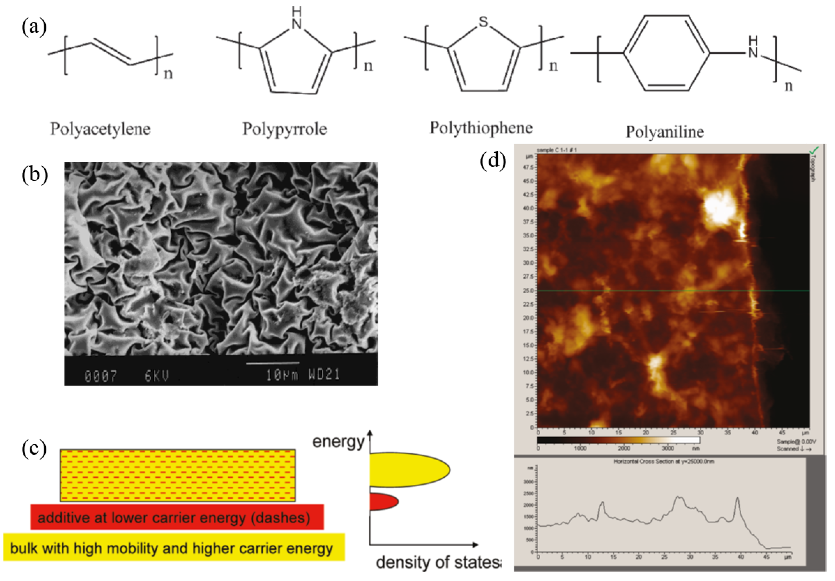
2.2.1. Polyacetylene and Polyaniline

Iodine-doped polyacetylene film showed the highest value of electrical conductivity of 1 × 10⁵ S/cm, which was better than that in non-doped polyacetylene film (3 × 10³ S/cm) [64]. Other metal chlorides, for example, FeCl3, MoCl5, NbCl5, and ZrCl4, have been doped with polyacetylene. The electrical conductivity and TE power of these doped polyacetylene films have been measured at different temperatures. The results demonstrated that FeCl3-doped polyacetylene film exhibited the highest value of electrical conductivity of 3 × 10⁵ S/cm at 220 K [65]. Besides, Bi0.5Sb1.5Te3 nanoplates embedded polyaniline composites presented highly increased Seebeck coefficient and thus an enhanced power factor from 16.5 × 10⁻⁸ to 84.4 × 10⁻⁸ W m−1 K−2 at 400 K [66]. However, the obvious disadvantage of polyacetylene is unstable in the atmosphere.
Searching for more stable conducting polymers, the electrically conductive emeraldine salt form of polyaniline is air stable, which is able to produce in large scale in low-cost [67,68]. The combination film of polyaniline with camphorsulfonic acid (CSA) showed good electrical conductivity between 10 K and 300 K. These thin films exhibit metallic conductivity due to the doping level. Among the different doping level, the 60% doped thin films have the electrical conductivity of 300 S/cm [69]. The multilayered polyaniline film (electrically insulating emeraldine based layers and electrically conducting CSA-doped emeraldine salt layers) even presented the higher ZT at 300 K than that of a bulk film of CSA-doped polyaniline [70].

2.2.2. Polypyrrole and Polythiophene

Polypyrrole, distinguished from above two conductive polymers, shows comparatively higher conductivity (>300 S/cm) at very low temperatures (T ~0 K). A series of polypyrrole samples from different synthesized methods measured the TE power and conductivity as a function of temperature, including chemically synthesized soluble polypyrrole films, wrinkled polypyrrole films on indium-tin-oxide electrodes, films were grown on nonconducting substrates, and polypyrrole gas sensors with different dopants. It turns out that the highest conductivity of 340 S/cm was obtained for polypyrrole that was doped with PF6 [71].
High-quality free-standing polythiophene and poly(3-methylthiophene) nanofilms with high tensile strength were investigated. They show a decent TE performance of ZT value of 0.03 at 250 K, which is higher than that of many other conducting polymers [72]. Sun et al. initially claimed that high conducting polymers tend to exhibit conductivity from carriers that are close to the Fermi level (Figure 2c). They fabricated poly(3-hexylthiophene) thin film on Si substrate and characterized the thickness of 100 nm (Figure 2d) [73]. Although the TE performance of this thin film was not particularly high, this work demonstrated a theoretical route for reaching a high Seebeck coefficient.

2.2.3. Poly(3,4-ethylenedioxythiophene)

Poly(3,4-ethylenedioxythiophene) is another extensively studied polymer, especially the combination of poly(3,4-ethylenedioxythiophene) and polystyrenesulfonate (PEDOT:PSS). The mixtures show high electrical conductivity along the casting plane [74]. For example, of 20 µm drop-cast films, the thermal and electrical in-plane conductivities are, respectively, 1.0 W m−1 K−1 and 500 S cm−1. The high electrical conductivity leads to a highly anisotropic thermal conductivity of drop-cast dimethylsulfoxide (DMSO)-mixed PEDOT: PSS films. When using DMSO post-treatment instead of DMSO addition in the PEDOT: PSS films, the power factor of the film is 65% increased. The electrical conductivity-improving contributes to this increase while the Seebeck coefficient is in minor change [75]. Besides, there is a significant enhancement of the electrical conductivity of PEDOT: PSS (from 787.99 to 4839.92 S cm−1) and Te-PEDOT:PSS hybrid (from 11.01 to 334.68 S cm−1) by chemical treatment with H2SO4 [76].

2.2.4. Other n-type Polymers

For n-type organic TE materials, poly(nickel-ethylenetetrathiolate) (poly(Ni-ett)) reaches the highest ZT value of 0.3 at room temperature [77]. An example shows that the optical power factor of poly(Ni-ett) synthesized at 0.6 V (131.6 μW m−1 K−2 at 360 K) is higher than that of at 1 or 1.6 V via potentiostatic deposition [78]. Poly(benzobisimidazobenzophenanthroline) (BBL) has demonstrated the electron mobility as high as 0.1 cm2 V−1 s−1 with the field-effect [79]. It can achieve 2.4 S cm−1 in the electrical conductivity [80]. As a new class of promising n-type organic TE materials, self-doping perylene diimide (PDI) derivatives has been reported with the power factor of 1.4 μW m−1 K−2 [81].

2.3. Inorganic-Organic Composite Thin Film TE Materials

Although conducting polymer thin films are low density, low cost, low thermal conductivity, and easy synthesis, it has not been feasible to apply these materials along in TE generators due to the limitations of electrical conductivity and ZT value. When combining inorganic materials and organic conducting polymers, both advantages from these two types of materials present significant potential for producing relatively low-cost and high-performance TE materials [82]. Recently, an increasing number of studies have reported on inorganic-organic thin film TE nanocomposite materials [83].

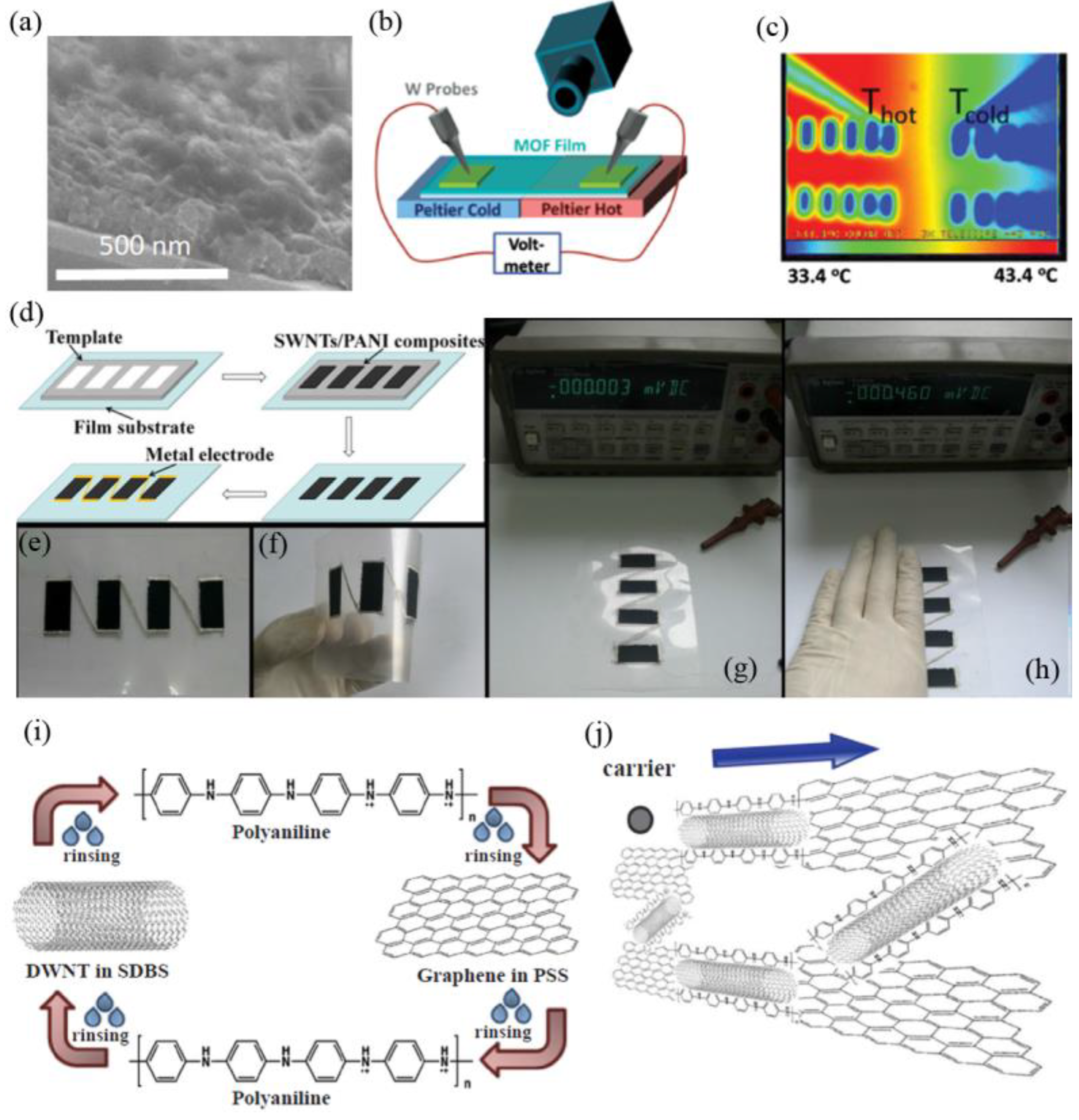
2.3.1. Metal-Organic Frameworks

Metal-organic frameworks (MOFs) start to be researched in TE application since its electrical conductivity has been reported [84,85]. Recently, the composite of tetracyanoquinodimethane (TCNQ) and Cu3(BTC)2 (BTC = benzene tricarboxylate) thin films that are deposited by a solution-based method at room temperature (Figure 3a). The TE properties of these TCNQ@Cu3(BTC)2 films were measured under the controlled temperature gradient, which shows the Seebeck coefficient of 375 µV/K at room temperature (Figure 3b,c). This value exceeds some organic thin films and even Bi2Te3 bulk materials [86]. However, the electrical performance of TCNQ@Cu3(BTC)2 film was lower than the above-mentioned TE materials. Although this work presents a new type of TE materials, the TE properties of MOFs films still need to improve.

2.3.2. Carbon Nanotube-Polymer Composites

Carbon nanotubes (CNTs), which are a new star of carbon materials, are increasingly used in TE composites or other energy storage materials due to their remarkable electrical property and low cost [89,90,91,92,93,94]. A good example is that an excellent flexible n-type and p-type single-walled CNTs (SWCNTs) networks film showed good power factor of 1.5 × 10³ and 1.84 × 10³ µW m−1 K−2, respectively, with a long working lifespan up to three months [25]. A novel technology for decreasing internal resistivity to assemble a flexible TE module based on these CNT films is initially demonstrated, which is different from previous works. Large-area thick p-type CNT films were fabricated firstly and then cut into stripes sticking on the substrate. Then, the CNT film stripe was covered alternately for remaining as p-type and converted uncovered part into n-type. In this technique, the p-n couples were creatively built in one stripe. Before measuring performance, pasting two metal electrodes for each edge. It is an improving inspiration for the design of flexible TE devices. The SWCNTs-polyaniline composite films were attempted in TE measurement, which presented the power factor was 217 µW m−1 K−2. In addition, 65 wt % SWCNTs-polyaniline composite segments that were prepared and assembled as a TE module, which can generate 10.4 µW m−1 K−2 of power efficiency with good stability in the air (Figure 3d–h) [87]. Further research reported that polyaniline/CNT/graphene multilayer film has a comparable power factor of 1.825 × 10³ µW m−1 K−2 at room temperature (Figure 3i,j) [88].
In conclusion, inorganic-based, organic-based, or inorganic-organic composites thin film TE materials present some obvious advantages, including improved power factor, better performance at room temperature, facile synthesis approaches, and low cost of production. Thus, they have great potential in the further development of flexible and portable TE devices.

3. Measurement Technique of Thin Film TE Materials

Different from TE measurements for bulk materials, the accurate characterization of TE performance in thin films is challenging. In 1958, T.C. Harman first published a measurement method, which is called the Harman method, utilized for measuring the ZT value in many works [95]. However, this method is not accurate for applying to thin films due to the slow thermal response of thin films and insensitive of small transient Seebeck voltage [96]. In much research, TE data of thin films were obtained using homemade apparatus for matching samples at different characteristics [97,98]. Thus, there is no uniform measurement method for all kinds of thin film TE materials. Because of that, some novel measurement techniques for electrical conductivity (σ), Seebeck coefficient (S), and thermal conductivity (κ), which will discuss as following, are developed for simple and more accurate characterization for thin films.

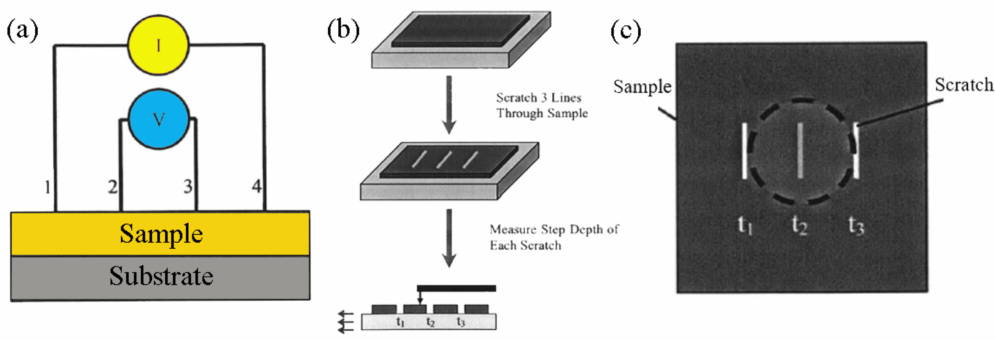
3.1. Electrical Conductivity

The electrical conductivity (σ) for thin films was measured with a four-point probe device. Although two-point measurement is generally used for bulk TE materials, the four-point method can eliminate any contact resistance during the measurement when considering the very thin thickness of the films (Figure 4a). Electrical conductivity can be calculated by the following equation:
σ = 1/ρ
ρ = (V/l)/[I/(wt)]
in which ρ is electrical resistivity, V and I are measured voltage and current, l is the length of electrons travel, and w and t are the width and thickness of a sample. The length (l) is the spacing of the probe tips and the width (w) is estimated by the software. The thickness (t) of each sample was measured with surface profilometry using a KLA Tencor P–16+ [99]. Firstly, three lines were scratched onto the sample without destroying the surface of the substrate (Figure 4b). Then, the step height was measured at each of these scratches. The thickness of the samples is estimated by the following equation:
t = {[(t1 + t3)/2] + t2}/2
For more accuracy, several electrical conductivity measurements will be taken near the center of the sample and calculate the average (Figure 4c).

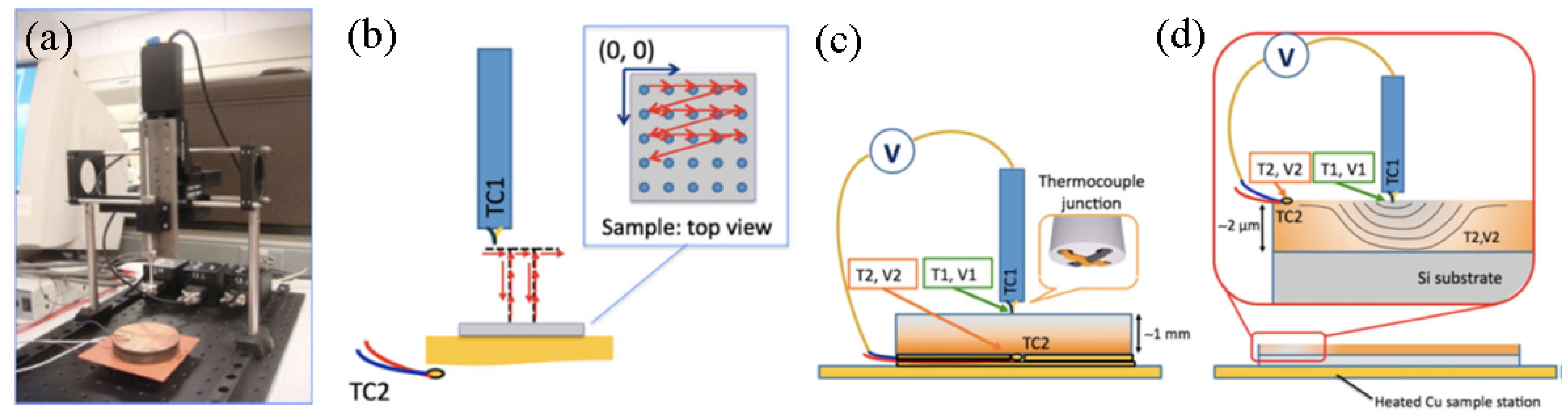
3.2. Seebeck Coefficient

In Snyder’s work, a scanning apparatus is reported to directly detect local variations of Seebeck coefficient on thin film samples. This scanning Seebeck coefficient measurement system is ideal for thin film samples, especially since it can measure films directly without separation from substrates [100]. A typical scanning Seebeck coefficient measurement system has a ‘‘hot probe’’ and a “cold probe”, in which they create the temperature gradient for the Seebeck coefficient measurement. In this setup, the heater is located on the sample holder side, and the cold (room-temperature) scanning probe acts as a cold finger. In Figure 5a, one probe keeps the same temperature and is electrically connected to the bottom of the sample surface and the other probe with a thermocouple junction at the tip contact with the film sample surface moving under the motorized stage. A simulated sample test process is shown in Figure 5b. The unique merit of this Seebeck coefficient measurement system is no requirement for substrate removal, which means that the homogeneity of the film sample deposited on an insulating substrate (or multilayer film insulated from a conducting substrate) can be directly evaluated. This merit simplifies the measurement steps and eliminates the possibility of sample degradation. Thus, the thermocouple junction is located onto the same surface where the scanning probe contacts, but at a different temperature determined by the substrate temperature, as shown in Figure 5c,d.

3.3. Thermal Conductivity

The experimental measurement of thermal conductivity (κ) for thin films, to some extent, results in a manifest error (~±10%) [101]. Some developed novel solutions can calibrate the experimental error and present fast measurement approaches. For instance, “steady-state isothermal technique” improves accuracy by collecting data under conditions where thermal losses and errors are unimportant. Analysis of this technique while using a Peltier cooler demonstrates the error of less than 1% [102]. When considering real TE generators, including qualitative demonstration, experimental uncertainty is reduced by this technique by more than a factor of 2. “Scanning hot-probe” and “lock-in transient Harman” methods reduce error by highly detailed treatment of interfacial contact effects, including electrical contact resistance and thermal contact effects. In scanning hot-probe technique, average probe temperature is also measured far from the sample to avoid the amount of heat loss. The heat transfer coefficient of “lock-in transient Harman” method was determined to be about 2%. Its uncertainty was assumed to be closer to 10% [103]. In addition, the thermal conductivity along the cross-plane and in-plane direction have been measured and reported by the 3ω methods and time-domain thermoreflectance measurements (TDTR) [26,55,74]. However, these two methods still need to be improved for the measurement of thin films with a relatively large surface roughness [62]. A self-heating 3ω method was used for solve the problem for the in-plane measurement where a gold wire with width should be thinner or comparable to the film thickness. In this method, the self-supported thin film with substrate acted both as a heater to create a temperature fluctuation and a sensor to measure the thermal response under a four-probe resistance measurement configuration (Figure 6a,b) [104].

4. Conclusions and Outlooks

In summary, traditional inorganic TE semi-conductive materials have been restricted, to some extent, in their stagnancy of performance and high cost. Although low-dimensional inorganic TE materials, such as superlattices and thin films, have been proved in decreasing thermal conductivity in many researches, the overall TE performance is insufficient to investigate TE devices. Furthermore, the TE working temperature of inorganic materials is usually above 500 K, which is the fatal weakness of these kind materials in the development of portable and wearable devices. The ideal TE devices are best served at room temperature or low temperature, which makes it easier to meet working temperature requirement.
When compared to inorganic materials, organic conducting polymer thin films have many features, including low cost, facile synthesis, lower working temperature, and low thermal conductivity, and they attract increasing attention. However, these organic polymer TE thin films still need to improve electrical conductivity and Seebeck coefficient in TE measurements.
Recently, the study of the combination of inorganic-organic composite TE materials is a possible strategy to meet breakthrough in intelligent TE devices, especially introducing high-performance inorganic TE materials into polymer thin films. The hybridization of CNTs or graphene and polymer thin films have been displayed amazing TE performance in many reports. As a recently developed strategy, inorganic-organic composite TE thin films is a promising direction for portable and wearable TE devices in the future, because they can achieve high TE performance, benefiting from both high electrical conductivity of inorganic materials and poor thermal conductivity of organic conducting polymers.
TE measurement technique, especially for thin films, is another hurdle to be conquered in the development of devices. Although it is sufficient that the theoretical fundamentals and experimental techniques of TE measurements in bulk materials, the measurement of thin films cannot rely solely on above theories and experimental techniques. In this case, a series of measurements of TE thin films are using a homemade apparatus for matching characteristics of samples. The accuracy of measured results is the priority of these research. Meantime, the improvement of measurement techniques is an auxiliary means to achieve the better performance of TE devices.
The interest in the development of portable and wearable TE devices will never terminate. As the inspiration of thin film TE materials, a prototype with liquid TE legs is under exploration, which can solve potential damage easily in the usage of TE devices. When compared with solid materials, liquid materials possess attractive advantages consisting of excellent deformability, ease of doping, and self–healing abilities, which could afford great promise for intelligent TE devices.

Funding

This project was funded by the National Natural Science Foundation of China (51702091, 51702046, 51772050, and 51432004), the Natural Science Foundation of Hubei Province, China (2017CFB192), the Innovation Program of Shanghai Municipal Education Commission (2017–01–07–00–03–E00025), the Shanghai Committee of Science and Technology, China (17ZR1401000, 18JC1411200 and 16JC1401800), China Postdoctoral Science Foundation (2017M621320), the Fundamental Research Funds for the Central Universities, the Programme of Introducing Talents of Discipline to Universities (111–2–04), DHU Distinguished Young Professor Program, Shanghai Pujiang Program (17PJ1400100), and State Key Laboratory for Modification of Chemical Fibers and Polymer Materials, Donghua University.

Conflicts of Interest

The authors declare no conflict of interest. The founding sponsors had no role in the design of the study; in the collection, analyses, or interpretation of data; in the writing of the manuscript, and in the decision to publish the results.

References

  1. Service, R.F. Temperature rises for devices that turn heat into electricity. Science 2004, 306, 806–807. [Google Scholar] [CrossRef] [PubMed]
  2. Lan, Y.; Minnich, A.J.; Chen, G.; Ren, Z. Enhancement of thermoelectric figure-of-merit by a bulk nanostructuring approach. Adv. Funct. Mater. 2010, 20, 357–376. [Google Scholar] [CrossRef]
  3. Nielsch, K.; Bachmann, J.; Kimling, J.; Böttner, H. Thermoelectric nanostructures: From physical model systems towards nanograined composites. Adv. Energy Mater. 2011, 1, 713–731. [Google Scholar] [CrossRef]
  4. Yang, J.; Shen, D.; Zhou, L.; Li, W.; Li, X.; Yao, C.; Wang, R.; El-Toni, A.M.; Zhang, F.; Zhao, D. Spatially confined fabrication of core-shell gold nanocages@mesoporous silica for near-infrared controlled photothermal drug release. Chem. Mater. 2013, 25, 3030–3037. [Google Scholar] [CrossRef]
  5. Yang, J.; Wang, Y.; Chou, S.; Zhang, R.; Xu, Y.; Fan, J.; Zhang, W.; Liu, H.; Zhao, D.; Dou, S. Yolk-shell silicon-mesoporous carbon anode with compact solid electrolyte interphase film for superior lithium-ion batteries. Nano Energy 2015, 18, 133–142. [Google Scholar] [CrossRef] [Green Version]
  6. Yang, J.; Wang, Y.; Li, W.; Wang, L.; Fan, Y.; Jiang, W.; Luo, W.; Wang, Y.; Kong, B.; Selomulya, C.; et al. Amorphous TiO2 shells: A vital elastic buffering layer on silicon nanoparticles for high-performance and safe lithium storage. Adv. Mater. 2017, 29, 1700523. [Google Scholar] [CrossRef] [PubMed]
  7. Wang, Q.; Zhao, Y.; Luo, W.; Jiang, W.; Fan, J.; Wang, L.; Jiang, W.; Zhang, W.; Yang, J. Iron nanoparticles in capsules: Derived from mesoporous silica-protected prussian blue microcubes as efficient selenium removal. Chem. Commum. 2018, 46, 5887–5890. [Google Scholar] [CrossRef] [PubMed]
  8. Minnich, A.J.; Dresselhaus, M.S.; Ren, Z.; Chen, G. Bulk nanostructured thermoelectric materials: Current research and future prospects. Energy Environ. Sci. 2009, 2, 466–479. [Google Scholar] [CrossRef]
  9. Snyder, G.J.; Toberer, E.S. Complex thermoelectric materials. Nat. Mater. 2008, 7, 105–114. [Google Scholar] [CrossRef] [PubMed]
  10. Bell, L.E. Cooling, heating, generating power, and recovering waste heat with thermoelectric systems. Science 2008, 321, 1457–1461. [Google Scholar] [CrossRef] [PubMed]
  11. Wu, Y.; Finefrock, S.W.; Yang, H. Nanostructured thermoelectric: Opportunities and challenges. Nano Energy 2012, 1, 651–653. [Google Scholar] [CrossRef]
  12. Vineis, C.J.; Shakouri, A.; Majumdar, A.; Kanatzidis, M.G. Nanostructured thermoelectrics: Big efficiency gains from small features. Adv. Mater. 2010, 22, 3970–3980. [Google Scholar] [CrossRef] [PubMed]
  13. Zhang, G.; Yu, Q.; Wang, W.; Li, X. Nanostructures for thermoelectric applications: Synthesis, growth mechanism, and property studies. Adv. Mater. 2010, 22, 1959–1962. [Google Scholar] [CrossRef] [PubMed]
  14. Seebeck, T.J. Ueber die magnetische polarisation der metalle and erze durch temperatur-differenz. Ann. Phys. 1821, 82, 133–160. (In Germany) [Google Scholar] [CrossRef]
  15. Qiu, P.; Shi, X.; Chen, L. Cu-based thermoelectric materials. Energy Storage Mater. 2016, 3, 85–97. [Google Scholar] [CrossRef]
  16. Dennler, G.; Chmielowski, R.; Jacob, S.; Capet, F.; Roussel, P.; Zastrow, S.; Nielsch, K.; Opahle, I.; Madsen, G.K.H. Are binary copper sulfides/selenides really new and promising thermoelectric materials? Adv. Energy Mater. 2014, 4, 1301581. [Google Scholar] [CrossRef]
  17. Han, C.; Sun, Q.; Li, Z.; Dou, S. Thermoelectric enhancement of different kinds of metal chalcogenides. Adv. Energy Mater. 2016, 6, 1600498. [Google Scholar] [CrossRef]
  18. Böttner, H.; Chen, G.; Venkatasubramanian, R. Aspects of thin-film superlattice thermoelectric materials, devices, and applications. MRS Bull. 2006, 31, 211–217. [Google Scholar] [CrossRef]
  19. Harman, T.C.; Taylor, P.J.; Walsh, M.P.; LaForge, B.E. Quantum dot superlattice thermoelectric materials and devices. Science 2002, 297, 2229–2232. [Google Scholar] [CrossRef] [PubMed]
  20. Zhao, W.; Liu, Z.; Sun, Z.; Zhang, Q.; Wei, P.; Mu, X.; Zhou, H.; Li, C.; Ma, S.; He, D.; et al. Superparamagnetic enhancement of thermoelectric performance. Nature 2017, 549, 247–251. [Google Scholar] [CrossRef] [PubMed]
  21. Chen, X.; Li, Z.; Dou, S. Ambient facile synthesis of gram-scale copper selenide nanostructures from commercial copper and selenium powder. ACS Appl. Mater. Interfaces 2015, 7, 13295–13302. [Google Scholar] [CrossRef] [PubMed]
  22. Chen, X.; Li, Z.; Yang, J.; Sun, Q.; Dou, S. Aqueous preparation of surfactant-free copper selenide nanowires. J. Colloid Interface Sci. 2015, 442, 140–146. [Google Scholar] [CrossRef] [PubMed] [Green Version]
  23. Zhang, L.; Chen, X.; Han, C. Application prospects of thermoelectric technique. Res. Dev. Mater. Sci. 2018, 3, 000571. [Google Scholar]
  24. Chen, Z.; Shi, X.; Zhao, L.; Zou, J. High-performance SnSe thermoelectric materials: Progress and future challenge. Prog. Mater. Sci. 2018, 97, 283–346. [Google Scholar] [CrossRef]
  25. Zhou, W.; Fan, Q.; Zhang, Q.; Cai, L.; Li, K.; Gu, X.; Yang, F.; Zhang, N.; Wang, Y.; Liu, H.; et al. High-performance and compact-designed flexible thermoelectric modules enabled by a reticulate carbon nanotube architecture. Nat. Commun. 2017, 8, 14886. [Google Scholar] [CrossRef] [PubMed] [Green Version]
  26. Bubnova, O.; Khan, Z.U.; Malti, A.; Braun, S.; Fahlman, M.; Berggren, M.; Crispin, X. Optimization of the thermoelectric figure of merit in the conducting polymer poly(3,4-ethylenedioxythiophene). Nat. Mater. 2011, 10, 429–433. [Google Scholar] [CrossRef] [PubMed]
  27. Lin, Z.; Hollar, C.; Kang, J.; Yin, A.; Wang, Y.; Shiu, H.; Huang, Y.; Hu, Y.; Zhang, Y.; Duan, X. A solution processable high-performance thermoelectric copper selenide thin film. Adv. Mater. 2017, 29, 1606662. [Google Scholar] [CrossRef] [PubMed]
  28. Yang, C.; Souchay, D.; Kneiss, M.; Bogner, M.; Wei, H.; Lorenz, M.; Oeckler, O.; Benstetter, G.; Fu, Y.; Grundmann, M. Transparent flexible thermoelectric material based on non-toxic earth-abundant p-type copper iodide thin film. Nat. Commun. 2017, 8, 16076. [Google Scholar] [CrossRef] [PubMed]
  29. Dresselhaus, M.S.; Chen, G.; Tang, M.; Yang, R.; Lee, H.; Wang, D.; Ren, Z.; Fleurial, J.P.; Gogna, P. New directions for low-dimensional thermoelectric materials. Adv. Mater. 2007, 19, 1043–1053. [Google Scholar] [CrossRef]
  30. Zhang, Q.; Ai, X.; Wang, L.; Chang, Y.; Luo, W.; Jiang, W.; Chen, L. Improved thermoelectric performance of silver nanoparticles-dispersed Bi2Te3 composites deriving from hierarchical two-phased heterostructure. Adv. Funct. Mater. 2015, 25, 966–976. [Google Scholar] [CrossRef]
  31. Venkatasubramanian, R.; Siivola, E.; Colpitts, T.; O’Quinn, B. Thin-film thermoelectric devices with high room-temperature figures of merit. Nature 2001, 413, 597–602. [Google Scholar] [CrossRef] [PubMed]
  32. Takashiri, M.; Shirakawa, T.; Miyazaki, K.; Tsukamoto, H. Fabrication and characterization of bismuth-telluride-based alloy thin film thermoelectric generators by flash evaporation method. Sens. Actuators A-Phys. 2007, 138, 329–334. [Google Scholar] [CrossRef]
  33. Venkatasubramanian, R.; Colpitts, T.; O’Quinn, B.; Liu, S.; El-Masry, N.; Lamvik, M. Low-temperature organometallic epitaxy and its application to superlattice structures in thermoelectrics. Appl. Phys. Lett. 1999, 75, 1104–1106. [Google Scholar] [CrossRef]
  34. Fan, P.; Li, Y.; Zheng, Z.; Lin, Q.; Luo, J.; Liang, G.; Zhang, M.; Chen, M. Thermoelectric properties optimization of al-doped ZnO thin films prepared by reactive sputtering Zn-Al alloy target. Appl. Surf. Sci. 2013, 284, 145–149. [Google Scholar] [CrossRef]
  35. Fan, P.; Zheng, Z.; Li, Y.; Lin, Q.; Luo, J.; Liang, G.; Cai, X.; Zhang, D.; Ye, F. Low-cost flexible thin film thermoelectric generator on zinc based thermoelectric materials. Appl. Phys. Lett. 2015, 106, 073901. [Google Scholar] [CrossRef]
  36. Teranishi, T.; Mori, Y.; Hayashi, H.; Kishimoto, A. Thermoelectric property of polycrystalline aluminum-doped zinc oxide enhanced by micropore foaming. J. Am. Ceram. Soc. 2012, 95, 690–695. [Google Scholar] [CrossRef]
  37. Ghosh, C.K.; Das, S.; Chattopadhyay, K.K. Enhancement of thermopower of Mn doped ZnO thin film. Phys. B Condens. Matter 2007, 399, 38–46. [Google Scholar] [CrossRef]
  38. Loureiro, J.; Neves, N.; Barros, R.; Mateus, T.; Santos, R.; Filonovich, S.; Reparaz, S.; Sotomayor-Torres, C.M.; Wyczisk, F.; Divay, L.; et al. Transparent aluminium zinc oxide thin films with enhanced thermoelectric properties. J. Mater. Chem. A 2014, 2, 6649–6655. [Google Scholar] [CrossRef] [Green Version]
  39. Chen, X.; Bai, Y.; Li, Z.; Wang, L.; Dou, S. Ambient synthesis of one-/two-dimensional CuAgSe ternary nanotubes as counter electrodes of quantum-dot-sensitized solar cells. ChemPlusChem 2016, 81, 414–420. [Google Scholar] [CrossRef]
  40. Chen, X.; Li, Z.; Bai, Y.; Sun, Q.; Wang, L.; Dou, S. Room-temperature synthesis of Cu2−xE (E = S, Se) nanotubes with hierarchical architecture as high-performance counter electrodes of quantum-dot-sensitized solar cells. Chem. Eur. J. 2015, 21, 1055–1063. [Google Scholar] [CrossRef] [PubMed]
  41. Tan, M.; Chen, X. Growth mechanism of single crystal nanowires of fcc metals (Ag, Cu, Ni) and hcp metal (Co) electrodeposited. J. Electrochem. Soc. 2012, 159, K15–K20. [Google Scholar] [CrossRef]
  42. Nunna, R.; Qiu, P.; Yin, M.; Chen, H.; Hanus, R.; Song, Q.; Zhang, T.; Chou, M.; Agne, M.T.; He, J.; et al. Ultrahigh thermoelectric performance in Cu2Se-based hybrid materials with highly dispersed molecular CNTs. Energy Environ. Sci. 2017, 10, 1928–1935. [Google Scholar] [CrossRef]
  43. Yang, C.; Kneiβ, M.; Lorenz, M.; Grundmann, M. Room-temperature synthesized copper iodide thin film as degenerate p-type transparent conductor with a boosted figure of merit. Proc. Natl. Acad. Sci. 2016, 113, 12929–12933. [Google Scholar] [CrossRef] [PubMed]
  44. Ohta, H. Thermoelectrics Based on Metal Oxide Thin Films. In Metal Oxide-Based Thin Film Structures: Formation, Characterization and Application of Interface-Based Phenomena, A Volume in Metal Oxides; Pryds, N., Esposito, V., Eds.; Elsevier: Amsterdam, The Netherlands, 2018; pp. 441–464. [Google Scholar]
  45. Ravichandran, J. Thermoelectric and thermal transport properties of complex oxide thin films, heterostructures and superlattices. J. Mater. Res. 2016, 32, 183–203. [Google Scholar] [CrossRef]
  46. Terasaki, I.; Sasago, Y.; Uchinokura, K. Large thermoelectric power in NaCo2O4 single crystals. Phys. Rev. B 1997, 56, 685–687. [Google Scholar] [CrossRef]
  47. Masset, A.C.; Michel, C.; Maignan, A.; Hervieu, M.; Toulemonde, O.; Studer, F.; Raveau, B. Misfit-layered cobaltite with an anisotropic giant magnetorsistance Ca3Co4O9. Phys. Rev. B 2000, 62, 166–175. [Google Scholar] [CrossRef]
  48. Paul, B.; Lu, J.; Eklund, P. Nanostructural tailoring to induce flexibility in thermoelectric Ca3Co4O9 thin films. ACS Appl. Mater. Interfaces 2017, 9, 25308–25316. [Google Scholar] [CrossRef] [PubMed]
  49. Paul, B.; Bjork, E.M.; Kumar, A.; Lu, J.; Eklund, P. Nanoporous Ca3Co4O9 thin films for transferable thermoelectrics. ACS Appl. Energy Mater. 2018, 1, 2261–2268. [Google Scholar] [CrossRef] [PubMed]
  50. Gushing, B.L.; Falster, A.U.; Simmons, W.B.; Wiley, J.B. A multivalent ion exchange route to lamellar calcium cobalt oxides CaxCoO2 (x ≤ 0.5). Chem. Commun. 1996, 23, 2635–2636. [Google Scholar] [CrossRef]
  51. Liu, J.; Huang, X.; Xu, G.; Chen, L. Thermoelectric properties of layered Sr0.29CoO2 crystals. J. Alloy. Compd. 2013, 576, 247–249. [Google Scholar] [CrossRef]
  52. Liu, J.; Huang, X.; Li, F.; Liu, R.; Chen, L. Low-temperature magnetic and thermoelectric properties of layered Ca0.33CoO2 crystals. J. Phys. Soc. Jpn. 2011, 80, 074802. [Google Scholar] [CrossRef]
  53. Liu, W.; Kim, H.; Jie, Q.; Ren, Z. Importance of high power factor in thermoelectric materials for power generation application a perspective. Scr. Mater. 2016, 111, 3–9. [Google Scholar] [CrossRef]
  54. Lévesque, I.; Bertrand, P.O.; Blouin, N.; Leclerc, M.; Zecchin, S.; Zotti, G.; Ratcliffe, C.I.; Klug, D.D.; Gao, X.; Gao, F.; et al. Synthesis and thermoelectric properties of polycarbazole, polyindolocarbazole, and polydiindolocarbazole derivatives. Chem. Mater. 2007, 19, 2128–2138. [Google Scholar] [CrossRef] [Green Version]
  55. Kim, G.H.; Shao, L.; Zhang, K.; Pipe, K.P. Engineered doping of organic semiconductors for enhanced thermoelectric efficiency. Nat. Mater. 2013, 12, 719–723. [Google Scholar] [CrossRef] [PubMed]
  56. Bubnova, O.; Khan, Z.U.; Wang, H.; Braun, S.; Evans, D.R.; Fabretto, M.; Hojati-Talemi, P.; Dagnelund, D.; Arlin, J.B.; Geerts, Y.H.; et al. Semi-metallic polymers. Nat. Mater. 2014, 13, 190–194. [Google Scholar] [CrossRef] [PubMed]
  57. Kolasinska, E.; Kolasinski, P. A review on electroactive polymers for waste heat recovery. Materials 2016, 9, 485. [Google Scholar] [CrossRef] [PubMed]
  58. Bubnova, O.; Crispin, X. Towards polymer-based organic thermoelectric generators. Energy Environ. Sci. 2012, 5, 9345–9362. [Google Scholar] [CrossRef]
  59. Shi, K.; Zhang, F.; Di, C.; Yan, T.; Zou, Y.; Zhou, X.; Zhu, D.; Wang, J.; Pei, J. Toward high performance n-type thermoelectric materials by rational modification of BDPPV backbones. J. Am. Chem. Soc. 2015, 137, 6979–6982. [Google Scholar] [CrossRef] [PubMed]
  60. Dubey, N.; Leclerc, M. Conducting polymers: Efficient thermoelectric materials. J. Polym. Sci. Polym. Phys. 2011, 49, 467–475. [Google Scholar] [CrossRef]
  61. Zhang, Q.; Sun, Y.; Xu, W.; Zhu, D. Organic thermoelectric materials: Emerging green energy materials converting heat to electricity directly and efficiently. Adv. Mater. 2014, 26, 6829–6851. [Google Scholar] [CrossRef] [PubMed]
  62. Sun, Y.; Qiu, L.; Tang, L.; Geng, H.; Wang, H.; Zhang, F.; Huang, D.; Xu, W.; Yue, P.; Guan, Y.; et al. Flexible n-type high-performance thermoelectric thin films of poly(nickel-ethylenetetrathiolate) prepared by an electrochemical method. Adv. Mater. 2016, 28, 3351–3358. [Google Scholar] [CrossRef] [PubMed]
  63. Xuan, Y.; Liu, X.; Desbief, S.; Leclère, P.; Fahlman, M.; Lazzaroni, R.; Berggren, M.; Cornil, J.; Emin, D.; Crispin, X. Thermoelectric properties of conducting polymers: The case of poly(3-hexylthiophene). Phys. Rev. B 2010, 82, 115454. [Google Scholar] [CrossRef]
  64. Zuzok, R.; Kaiser, A.B.; Pukacki, W.; Roth, S. Thermoelectric power and conductivity of iodine-doped ‘‘new’’ polyacetylene. J. Chem. Phys. 1991, 95, 1270–1275. [Google Scholar] [CrossRef]
  65. Park, Y.W.; Yoon, C.O.; Na, B.C.; Shirakawa, H.; Akagi, K. Metallic properties of transition metal halides doped polyacetylene: The soliton liquid state. Synth. Met. 1991, 41, 27–32. [Google Scholar] [CrossRef]
  66. Guo, C.; Chu, F.; Chen, P.; Zhu, J.; Wang, H.; Wang, L.; Fan, Y.; Jiang, W. Effectively enhanced thermopower in polyaniline/Bi0.5Sb1.5Te3 nanoplate composites via carrier energy scattering. J. Mater. Sci. 2018, 53, 6752–6762. [Google Scholar] [CrossRef]
  67. Li, J.; Tang, X.; Li, H.; Yan, Y.; Zhang, Q. Synthesis and thermoelectric properties of hydrochloric acid-doped polyaniline. Synth. Met. 2010, 160, 1153–1158. [Google Scholar] [CrossRef]
  68. Sun, Y.; Wei, Z.; Xu, W.; Zhu, D. A three-in-one improvement in thermoelectric properties of polyaniline brought by nanostructures. Synth. Met. 2010, 160, 2371–2376. [Google Scholar] [CrossRef]
  69. Holland, E.R.; Pomfret, S.J.; Adams, P.N.; Abell, L.; Monkman, A.P. Doping dependent transport properties of polyaniline-CSA films. Synth. Met. 1997, 84, 777–778. [Google Scholar] [CrossRef]
  70. Tlshima, N. Conductive polymers as a new type of thermoelectric material. Macromol. Symp. 2002, 186, 81–86. [Google Scholar] [CrossRef]
  71. Kemp, N.T.; Kaiser, A.B.; Liu, C.; Chapman, B.; Mercier, O.; Carr, A.M.; Trodahl, H.J.; Buckley, R.G.; Partridge, A.C.; Lee, J.; et al. Thermoelectric power and conductivity of different types of polypyrrole. J. Polym. Sci. Part B Polym. Phys. 1999, 37, 953–960. [Google Scholar] [CrossRef]
  72. Lu, B.; Liu, C.; Lu, S.; Xu, J.; Jiang, F.; Li, Y.; Zhang, Z. Thermoelectric performances of free-standing polythiophene and poly(3-methylthiophene) nanofilms. Chin. Phys. Lett. 2010, 27, 057201. [Google Scholar]
  73. Sun, J.; Yeh, M.L.; Jung, B.J.; Zhang, B.; Feser, J.; Majumdar, A.; Katz, H.E. Simultaneous increase in Seebeck coefficient and conductivity in a doped poly(alkylthiophene) blend with defined density of states. Macromolecules 2010, 43, 2897–2903. [Google Scholar] [CrossRef]
  74. Liu, J.; Wang, X.; Li, D.; Coates, N.E.; Segalman, R.A.; Cahill, D.G. Thermal conductivity and elastic constants of PEDOT:PSS with high electrical conductivity. Macromolecules 2015, 48, 585–591. [Google Scholar] [CrossRef]
  75. Luo, J.; Billep, D.; Waechtler, T.; Otto, T.; Toader, M.; Gordan, O.; Sheremet, E.; Martin, J.; Hietschold, M.; Zahn, D.R.T.; et al. Enhancement of the thermoelectric properties of PEDOT:PSS thin films by post-treatment. J. Mater. Chem. A 2013, 1, 7576–7583. [Google Scholar] [CrossRef]
  76. Bae, E.J.; Kang, Y.H.; Jang, K.S.; Cho, S.Y. Enhancement of thermoelectric properties of PEDOT:PSS and tellurium-PEDOT:PSS hybrid composites by simple chemical treatment. Sci. Rep. 2016, 6, 18805. [Google Scholar] [PubMed]
  77. Di, C.A.; Xu, W.; Zhu, D.B. Organic thermoelectrics for green energy. Natl. Sci. Rev. 2016, 3, 269–271. [Google Scholar] [CrossRef] [Green Version]
  78. Sun, Y.; Zhang, J.; Liu, L.; Qin, Y.; Sun, Y.; Xu, W.; Zhu, D. Optimization of the thermoelectric properties of poly(nickel-ethylenetetrathiolate) synthesized via potentiostatic deposition. Sci. China Chem. 2016, 59, 1323–1329. [Google Scholar] [CrossRef]
  79. Babel, A.; Jenekhe, S.A. High electron mobility in ladder polymer field-effect transistors. J. Am. Chem. Soc. 2003, 125, 13656–13657. [Google Scholar] [CrossRef] [PubMed]
  80. Wang, S.; Sun, H.; Ail, U.; Vagin, M.; Persson, P.O.A.; Andreasen, J.W.; Thiel, W.; Berggren, M.; Crispin, X.; Fazzi, D.; et al. Thermoelectric properties of solution-processed n-doped ladder-type conducting polymers. Adv. Mater. 2016, 28, 10764–10771. [Google Scholar] [CrossRef] [PubMed]
  81. Russ, B.; Robb, M.J.; Brunetti, F.G.; Miller, P.L.; Perry, E.E.; Patel, S.N.; Ho, V.; Chang, W.B.; Urban, J.J.; Chabinyc, M.L.; et al. Power factor enhancement in solution-processed organic n-type thermoelectrics through molecular design. Adv. Mater. 2014, 26, 3473–3477. [Google Scholar] [CrossRef] [PubMed]
  82. Du, Y.; Shen, S.Z.; Cai, K.F.; Casey, P.S. Research progress on polymer–inorganic thermoelectric nanocomposite materials. Prog. Polym. Sci. 2012, 37, 820–841. [Google Scholar] [CrossRef]
  83. Wan, C.; Gu, X.; Dang, F.; Itoh, T.; Wang, Y.; Sasaki, H.; Kondo, M.; Koga, K.; Yabuki, K.; Snyder, G.J.; et al. Flexible n-type thermoelectric materials by organic intercalation of layered transition metal dichalcogenide TiS2. Nat. Mater. 2015, 14, 622–627. [Google Scholar] [CrossRef] [PubMed]
  84. Sun, L.; Miyakai, T.; Seki, S.; Dincă, M. Mn2(2,5-disulfhydrylbenzene-1,4-dicarboxylate): A microporous metal-organic framework with infinite (−Mn–S−) chains and high intrinsic charge mobility. J. Am. Chem. Soc. 2013, 135, 8185–8188. [Google Scholar] [CrossRef] [PubMed]
  85. Sheberla, D.; Sun, L.; Blood-Forsythe, M.A.; Er, S.; Wade, C.R.; Brozek, C.K.; Aspuru-Guzik, A.; Dinca, M. High electrical conductivity in Ni3(2,3,6,7,10,11-hexaiminotriphenylene)2, a semiconducting metal-organic graphene analogue. J. Am. Chem. Soc. 2014, 136, 8859–8862. [Google Scholar] [CrossRef] [PubMed]
  86. Erickson, K.J.; Leonard, F.; Stavila, V.; Foster, M.E.; Spataru, C.D.; Jones, R.E.; Foley, B.M.; Hopkins, P.E.; Allendorf, M.D.; Talin, A.A. Thin film thermoelectric metal-organic framework with high Seebeck coefficient and low thermal conductivity. Adv. Mater. 2015, 27, 3453–3459. [Google Scholar] [CrossRef] [PubMed]
  87. Wang, L.; Yao, Q.; Xiao, J.; Zeng, K.; Qu, S.; Shi, W.; Wang, Q.; Chen, L. Engineered molecular chain ordering in single-walled carbon nanotubes/polyaniline composite films for high-performance organic thermoelectric materials. Chem. Asian J. 2016, 11, 1804–1810. [Google Scholar] [CrossRef] [PubMed]
  88. Cho, C.Y.; Stevens, B.; Hsu, J.H.; Bureau, R.; Hagen, D.A.; Regev, O.; Yu, C.H.; Grunlan, J.C. Completely organic multilayer thin film with thermoelectric power factor rivaling inorganic tellurides. Adv. Mater. 2015, 27, 2996–3001. [Google Scholar] [CrossRef] [PubMed]
  89. Meng, C.; Liu, C.; Fan, S. A promising approach to enhanced thermoelectric properties using carbon nanotube networks. Adv. Mater. 2010, 22, 535–539. [Google Scholar] [CrossRef] [PubMed]
  90. Yao, Q.; Chen, L.; Zhang, W.; Liufu, S.C.; Chen, X. Enhanced thermoelectric performance of single-walled carbon nanotubes/polyaniline hybrid nanocomposites. ACS Nano 2010, 4, 2445–2451. [Google Scholar] [CrossRef] [PubMed]
  91. Luo, W.; Chen, X.; Xia, Y.; Chen, M.; Wang, L.; Wang, Q.; Li, W.; Yang, J. Surface and interface engineering of silicon-based anode materials for lithium-ion batteries. Adv. Energy Mater. 2017, 7, 1701083. [Google Scholar] [CrossRef]
  92. Luo, W.; Shen, D.; Zhang, R.; Zhang, B.; Wang, Y.; Dou, S.; Liu, H.; Yang, J. Germanium nanograin decoration on carbon shell: Boosting lithium-storage properties of silicon nanoparticles. Adv. Funct. Mater. 2016, 26, 7800–7806. [Google Scholar] [CrossRef]
  93. Luo, W.; Wang, Y.; Chou, S.; Xu, Y.; Li, W.; Kong, B.; Dou, S.; Liu, H.; Yang, J. Critical thickness of phenolic resin-based carbon interfacial layer for improving long cycling stability of silicon nanoparticle anodes. Nano Energy 2016, 27, 255–264. [Google Scholar] [CrossRef]
  94. Luo, W.; Wang, Y.; Wang, L.; Jiang, W.; Chou, S.; Dou, S.; Liu, H.; Yang, J. Silicon/mesoporous carbon/crystalline TiO2 nanoparticles for highly stable lithium storage. ACS Nano 2016, 10, 10524–10532. [Google Scholar] [CrossRef] [PubMed]
  95. Harman, T.C. Special techniques for measurement of thermoelectric properties. J. Appl. Phys. 1958, 29, 1373–1374. [Google Scholar] [CrossRef]
  96. Singh, R.; Bian, Z.X.; Shakouri, A.; Zeng, G.H.; Bahk, J.H.; Bowers, J.E.; Zide, J.M.O.; Gossard, A.C. Direct measurement of thin-film thermoelectric figure of merit. Appl. Phys. Lett. 2009, 94, 212508. [Google Scholar] [CrossRef] [Green Version]
  97. Suarez, F.; Parekh, D.P.; Ladd, C.; Vashaee, D.; Dickey, M.D.; Öztürk, M.C. Flexible thermoelectric generator using bulk legs and liquid metal interconnects for wearable electronics. Appl. Energy 2017, 202, 736–745. [Google Scholar] [CrossRef]
  98. Jia, H.; Tao, X.; Wang, Y. Flexible and self-healing thermoelectric converters based on thermosensitive liquids at low temperature gradient. Adv. Electron. Mater. 2016, 2, 1600136. [Google Scholar] [CrossRef]
  99. Kuryak, C.A. Nanostructured Thin Film Thermoelectric Composite Materials Using Conductive Polymer PEDOT:PSS. Master’s Thesis, Massachusetts Institute of Technology, Cambridge, MA, USA, April 2013. [Google Scholar]
  100. Iwanaga, S.; Snyder, G.J. Scanning Seebeck coefficient measurement system for homogeneity characterization of bulk and thin-film thermoelectric materials. J. Electron. Mater. 2012, 41, 1667–1674. [Google Scholar] [CrossRef]
  101. Wang, H.; Porter, W.D.; Böttner, H.; König, J.; Chen, L.D.; Bai, S.Q.; Tritt, T.M.; Mayolet, A.; Senawiratne, J.; Smith, C.; et al. Transport properties of bulk thermoelectrics—An international round-robin study. Part I: Seebeck coefficient and electrical resistivity. J. Electron. Mater. 2013, 42, 654–664. [Google Scholar] [CrossRef]
  102. Taylor, P.J.; Maddux, J.R.; Uppal, P.N. Measurement of thermal conductivity using steady-state isothermal conditions and validation by comparison with thermoelectric device performance. J. Electron. Mater. 2012, 41, 2307–2312. [Google Scholar] [CrossRef]
  103. Taylor, P.J.; Wilson, A.; Maddux, J.R.; Borca-Tasciuc, T.; Moran, S.P.; Castillo, E.; Borca-Tasciuc, D. Novel measurement methods for thermoelectric power generator materials and devices. In Thermoelectrics for Power Generation—A Look at Trends in the Technology; Skipidarov, S., Nikitin, M., Eds.; INTECH: London, UK, 2016; pp. 389–434. [Google Scholar]
  104. Lu, L.; Yi, W.; Zhang, D. 3ω method for specific heat and thermal conductivity measurements. Rev. Sci. Instrum. 2001, 72, 2996–3003. [Google Scholar] [CrossRef]
Figure 1. (a) Temperature dependence of figure of merit (ZT) of 10 Å/50 Å p-type Bi2Te3/Sb2Te3 superlattice compared to those of several recently reported materials. Reproduced from [31] with permission; Copyright Nature Publishing Group 2001; Schematic illustration (b) and photograph (c) of the bismuth-telluride-based alloy thin film thermoelectric (TE) generator. Reproduced [32] with permission; Copyright Elsevier 2007; Schematic illustration of the Zn based thin film TE generator (TFTEG): (d) A p-n couple was formed through connecting the n-type Al-doped ZnO and p-type Zn-Sb based thin films by metal layer bonding with Cu films deposited on both sides of the substrate; (e) Structure of the whole TFTEG; (f) and (g) are pictures of real Zn based TFTEG products. Reproduced [35] with permission; Copyright AIP Publishing 2015; (h) Cross-section scanning electron microscopic (SEM) image of the Cu2Se thin film on Al2O3 substrate; (i) Photograph of the Cu2Se thin film on the polyimide substrate. Reproduced [27] with permission; Copyright John Wiley & Sons, Inc. 2017; (j) The photograph of a CuI thin film sample deposited on polyethylene terephthalate (PET) substrate with a bending angle; (k) Schematic illustration for the power output measurement of the CuI/PET single-leg TE device; and, (l) The example infrared image taken during one of the measurements. Reproduced from [28] with permission; Copyright Nature Publishing Group 2017.
Coatings 08 00244 g001
Figure 2. (a) Chemical structures of polyacetylene, polyaniline, polypyrrole, and polythiophene. Reproduced from [61] with permission; Copyright John Wiley & Sons, Inc. 2014; (b) SEM image of the surface of a polypyrrole film (doped with PF6) that was facing the ITO (indium tin oxide) electrode. Reproduced from [71] with permission; Copyright John Wiley & Sons, Inc. 1999; (c) Schematic illustration of proposed organic TE composite, consisting of an additive that sets the Fermi level and a bulk in which charge carriers at higher energy levels are transported; and (d) Atomic force microscope (AFM) image of drop-cast blend poly(3-hexylthiophene) thin film on Si substrate. Reproduced from [73] with permission; Copyright American Chemical Society 2010.
Coatings 08 00244 g002
Figure 3. (a) Cross-section SEM image of an infiltrated tetracyanoquinodimethane (TCNQ)@Cu3(BTC)2 thin film; (b) Schematic illustration of the TE measurement for metal-organic frameworks (MOF) thin film. An infrared (IR) camera is used to measure the temperature difference between heat side and cool side of the substrate and a multimeter is detected for the voltage generated between two of the metal contacts; (c) Example IR image taken during one of the measurements. Reproduced from [86] with permission; Copyright John Wiley & Sons, Inc. 2015; (d) Method for the preparation and assembly of the single-walled carbon nanotubes (SWCNTs)-polyaniline composite thin film TE module; (e,f) Photograph of fabricated flexible TE module; (g,h) Thermal voltage generation from the TE module before and after touching at one side of the module; Reproduced from [87] with permission; Copyright John Wiley & Sons, Inc. 2016; (i) Schematic illustration of the layer-by-layer self-assembly procedure of polyaniline/CNT/graphene multilayer film; and (j) carrier transport in these multilayer film. Reproduced from [88] with permission; Copyright John Wiley & Sons, Inc. 2015.
Coatings 08 00244 g003
Figure 4. (a) Four-point electrical conductivity circuit. Current is supplied between pin 1 to pin 4, while voltage is measured between pin 2 to pin 3; (b) The process and locations of thickness measurements using the profilometer; and (c) The electrical conductivity measurement area of the sample. Reproduced from [99] with permission; Copyright Massachusetts Institute of Technology 2013.
Coatings 08 00244 g004
Figure 5. (a) Photograph of the scanning Seebeck coefficient measurement system and (b) schematic illustration of the scanning tip routes; Schematic illustration of the setup for (c) bulk and (d) thin-film samples. Reproduced from [100] with permission; Copyright Springer 2012.
Coatings 08 00244 g005
Figure 6. (a) Schematic illustration of the four-probe configuration for measuring the specific heat and thermal conductivity of a filament-like specimen; and (b) The four-probe configuration on the specimen holder for measuring the in-plane thermal conductivity of the film. Reproduced from [62] with permission; Copyright John Wiley & Sons, Inc. 2016.
Coatings 08 00244 g006

