Effects of Annealing on Residual Stress in Ta2O5 Films Deposited by Dual Ion Beam Sputtering

 ,
,
Abstract
:1. Introduction
2. Experimental Details
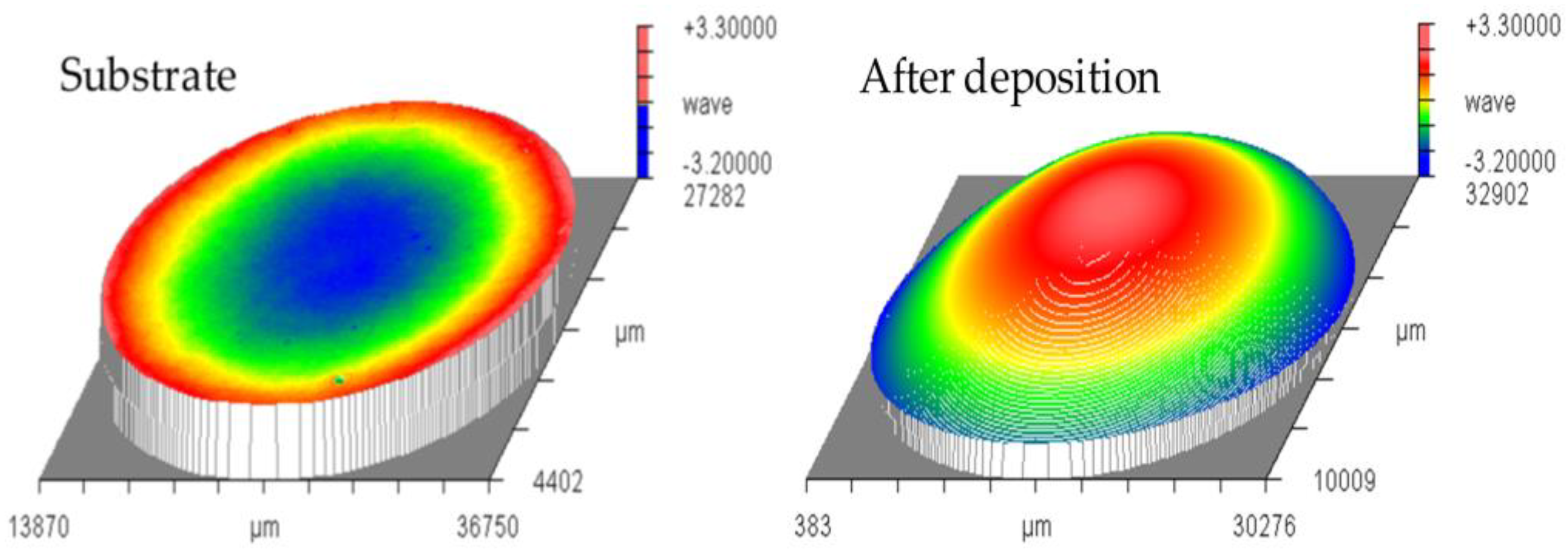
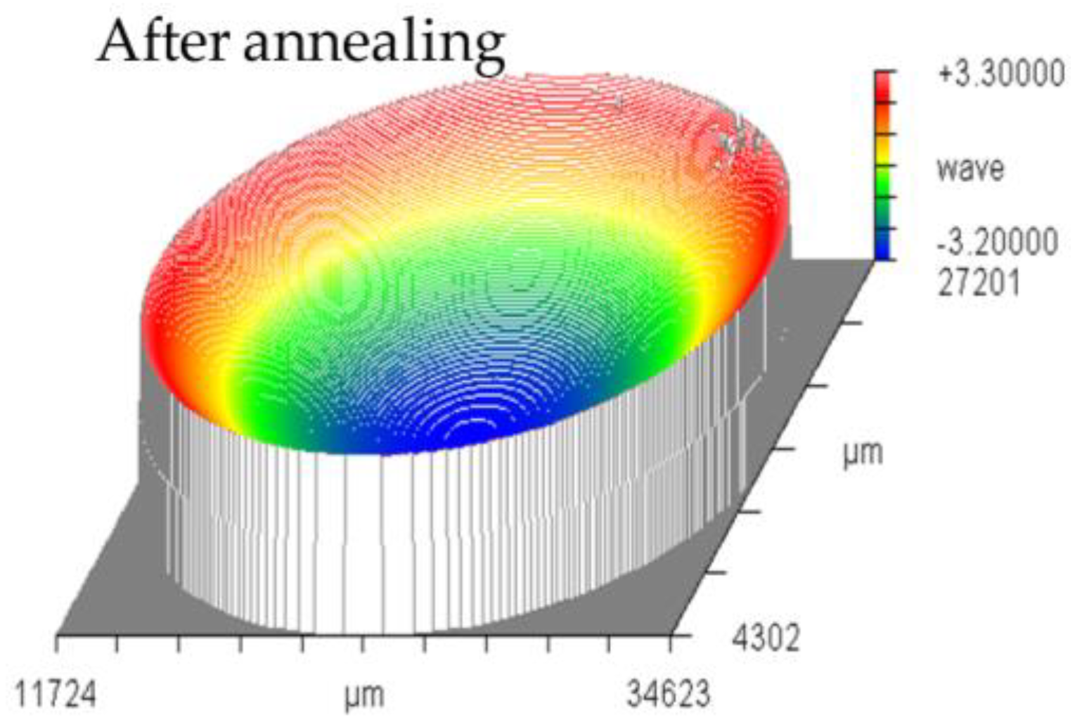
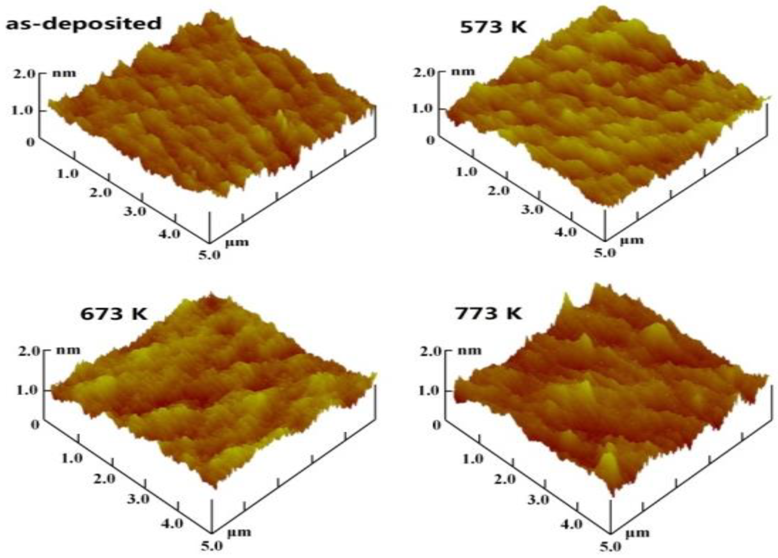
3. Results and Discussion
4. Conclusions
Supplementary Materials
Acknowledgments
Author Contributions
Conflicts of Interest
References
- Sun, R.C.; Tisone, T.C.; Cruzan, P.D. The origin of internal stress in low−voltage sputtered tungsten films. J. Appl. Phys. 1975, 46, 112–117. [Google Scholar] [CrossRef]
- Hsueh, C.H. Thermal stresses in elastic multilayer systems. Thin Solid Films 2002, 418, 182–188. [Google Scholar] [CrossRef]
- Ennos, A.E. Stresses developed in optical film coatings. Appl. Opt. 1966, 5, 51–61. [Google Scholar] [CrossRef] [PubMed]
- Yoon, S.G.; Kim, Y.T.; Kim, H.K.; Kim, M.J.; Lee, H.M.; Yoon, D.H. Comparision of residual stress and optical properties in Ta2O5 thin films deposited by single and dual ion beam sputtering. Mater. Sci. Eng. B 2005, 118, 234–237. [Google Scholar] [CrossRef]
- Wang, J.; Maier, R.L. Correlation between mechanical stress and optical properties of SiO2/Ta2O5 multilayer UV narrow-bandpass filters deposited by plasma ion-assisted deposition. In Advances in Thin-Film Coatings for Optical Applications II, Proceedings of Optics and Photonics 2005, San Diego, CA, USA, 31 July–4 August 2005; Fulton, M.L., Kruschwitz, J.D.T., Eds.; SPIE: Bellingham, WA, USA, 2005; p. 58700E. [Google Scholar]
- Deng, S.W.; Wang, F.; Liu, S.F.; Li, G.; Sun, L.; Jin, Y.Q. Residual stress prediction and control of Ta2O5/SiO2 multilayer based on layer structure designing. Chin. Opt. Lett. 2013, 11, S10701. [Google Scholar] [CrossRef]
- Atanassova, E.; Tyuliev, G.; Paskaleva, A.; Spassov, D.; Kostov, K. XPS study of N2 annealing effect on thermal Ta2O5 layers on Si. Appl. Surf. Sci. 2004, 225, 86–99. [Google Scholar] [CrossRef]
- Atanassova, E.; Dimitrova, T.; Koprinarova, J. AES and XPS study of thin RF-sputtered Ta2O5 layers. Appl. Surf. Sci. 1995, 84, 193–202. [Google Scholar] [CrossRef]
- Teixeira, V. Residual stress and cracking in thin PVD coatings. Vacuum 2002, 64, 393–399. [Google Scholar] [CrossRef]
- Brown, J.T. Center wavelength shift dependence on substrate coefficient of thermal expansion for optical thin-film interference filters deposited by ion-beam sputtering. Appl. Opt. 2004, 43, 4506–4511. [Google Scholar] [CrossRef] [PubMed]
- Cosar, M.B.; Ozhan, A.E.S.; Aydogdu, G.H. Improving the laser damage resistance of oxide thin films and multilayers via tailoring ion beam sputtering parameters. Appl. Surf. Sci. 2015, 336, 34–38. [Google Scholar] [CrossRef]
- Forest, D.; Ganau, P.; Lagrange, B.; Mackowski, J.M.; Michel, C.; Montorio, J.L.; Morgado, N.; Pignard, R.; Pinard, L.; Remillieux, A.I.B.S. Coatings on large substrates: Towards an improvement of the mechanical and optical performances. In Proceedings of the Optical Interference Coatings, Tucson, AZ, USA, 27 June 2004; p. MB7. [Google Scholar]
- Martin, I.W.; Nawrodt, R.; Craig, K.; Schwarz, C.; Bassiri, R.; Harry, G.; Hough, J.; Penn, S.; Reid, S.; Robie, R.; et al. Low temperature mechanical dissipation of an ion-beam sputtered silica film. Class. Quant. Grav. 2014, 31, 35019–35030. [Google Scholar] [CrossRef]
- Stolz, C.; Weinzapfel, C.; Rogowski, G.T.; Smith, D.; Rigatti, A.; Oliver, J.; Taniguch, J. Status of optical coatings for the national ignition facility. In Proceedings of the Optical Interference Coatings, Banff, AB, Canada, 15 July 2001; p. ThD3. [Google Scholar]
- Netterfield, R.P.; Gross, M.; Baynes, F.N.; Green, K.L.; Harry, G.M.; Armandula, H.; Rowan, S.; Hough, J.; Crooks, D.R.M.; Fejer, M.M.; et al. Low mechanical loss coatings for LIGO optics: Progress report. In Advances in Thin-Film Coatings for Optical Applications II, Proceedings of Optics and Photonics 2005, San Diego, CA, USA, 31 July–4 August 2005; Fulton, M.L., Kruschwitz, J.D.T., Eds.; SPIE: Bellingham, WA, USA, 2005; p. 58700H. [Google Scholar]
- Bischoff, M.; Nowitzki, T.; Voß, O.; Wilbrandt, S.; Stenzel, O. Postdeposition treatment of IBS coatings for UV applications with optimized thin-film stress properties. Appl. Opt. 2014, 53, A212–A220. [Google Scholar] [CrossRef]
- Xu, C.; Xiao, Q.; Ma, J.; Jin, Y.; Shao, J.; Fan, Z. High temperature annealing effect on structure, optical property and laser-induced damage threshold of Ta2O5 films. Appl. Surf. Sci. 2008, 254, 6554–6559. [Google Scholar] [CrossRef]
- Qiao, Z.; Pu, Y.; Liu, H.; Luo, K.; Wang, G.; Liu, Z.; Ma, P. Residual stress and laser-induced damage of ion-beam sputtered Ta2O5/SiO2 mixture coatings. Thin Solid Films 2015, 592, 221–224. [Google Scholar] [CrossRef]
- Shang, P.; Xiong, S.; Li, L.; Tian, D.; Ai, W. Investigation on thermal stability of Ta2O5, TiO2 and Al2O3 coatings for application at high temperature. Appl. Surf. Sci. 2013, 285, 713–720. [Google Scholar] [CrossRef]
- Tien, C.L. Influence of ejection angle on residual stress and optical properties of sputtering Ta2O5 thin films. Appl. Surf. Sci. 2008, 255, 2890–2895. [Google Scholar] [CrossRef]
- Tang, C.J.; Jaing, C.C.; Lee, K.S.; Lee, C.C. Residual stress in Ta2O5-SiO2 composite thin-film rugate filters prepared by radio frequency ion-beam sputtering. Appl. Opt. 2008, 47, 167–171. [Google Scholar] [CrossRef]
- Stenzel, O.; Wilbrandt, S.; Kaiser, N.; Vinnichenko, M.; Munnik, F.; Kolitsch, A.; Chuvilin, A.; Kaiser, U.; Ebert, J.; Jakobs, S. The correlation between mechanical stress, thermal shift and refractive index in HfO2, Nb2O5, Ta2O5 and SiO2 layers and its relation to the layer porosity. Thin Solid Films 2009, 517, 6058–6068. [Google Scholar] [CrossRef]
- Yoon, S.G.; Kang, S.M.; Yoon, D.H. Post-annealing effects on the structural properties and residual stress of Ta2O5 thin films deposited by ion beam sputtering. J. Optoelectron. Adv. Mater. 2007, 9, 1246–1249. [Google Scholar]
- Zhao, Y.A.; Wang, Y.J.; Gong, H.; Shao, J.D.; Fan, Z.X. Annealing effects on structure and laser-induced damage threshold of Ta2O5/SiO2 dielectric mirrors. Appl. Surf. Sci. 2003, 210, 353–358. [Google Scholar] [CrossRef]
- Xu, C.; Li, D.W.; Fan, H.L.; Deng, J.X.; Qi, J.W.; Yi, P.; Qiang, Y.H. Effects of different post-treatment methods on optical properties, absorption and nanosecond laser-induced damage threshold of Ta2O5 films. Thin Solid Films 2015, 580, 12–20. [Google Scholar] [CrossRef]
- Xu, C.; Yang, S.; Zhang, S.; Niu, J.; Qiang, Y.; Liu, J.; Li, D. Temperature dependences of optical properties, chemical composition, structure and laser damage in Ta2O5 films. Chin. Phys. B 2012, 21, 297–305. [Google Scholar] [CrossRef]
- Born, M.; Wolf, E. Electromagnetic potentials and polarization. In Principles of Optics; Pergamon: London, UK, 1959; p. 986. [Google Scholar]
- Stoney, G.G. The tension of metallic films deposited by electrolysis. Proc. R. Soc. Lond. A 1909, 82, 40–43. [Google Scholar] [CrossRef]
- Kičas, S.; Gimževskis, U.; Melnikas, S. Post deposition annealing of IBS mixture coatings for compensation of film induced stress. Opt. Mater. Express 2016, 6, 2236–2243. [Google Scholar] [CrossRef]


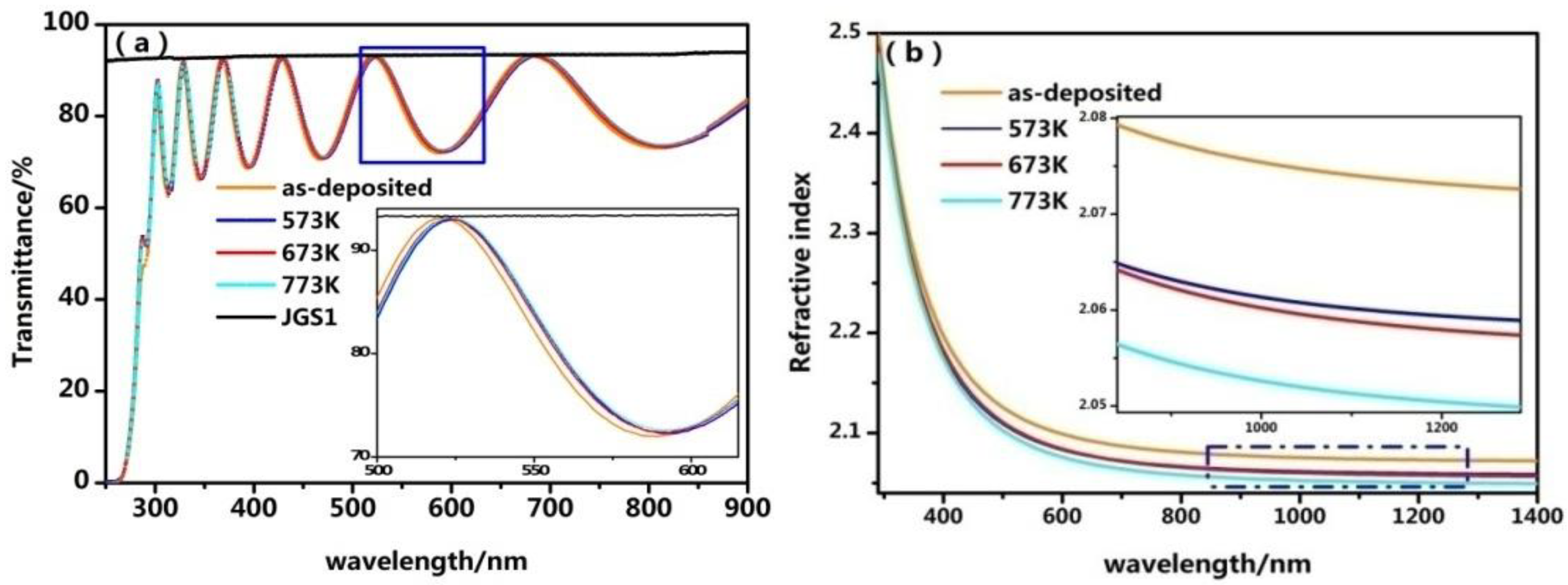
| Sample | Temperature/K | nf | k/10−3 | P | Surface Roughness (Rms)/nm |
|---|---|---|---|---|---|
| #1 | as-deposited | 2.10 | 0.7 | 0.96 | 0.17 |
| #2 | 573 | 2.09 | 0.5 | 0.95 | 0.17 |
| #3 | 673 | 2.09 | 0.27 | 0.95 | 0.19 |
| #4 | 773 | 2.08 | 0.1 | 0.94 | 0.24 |
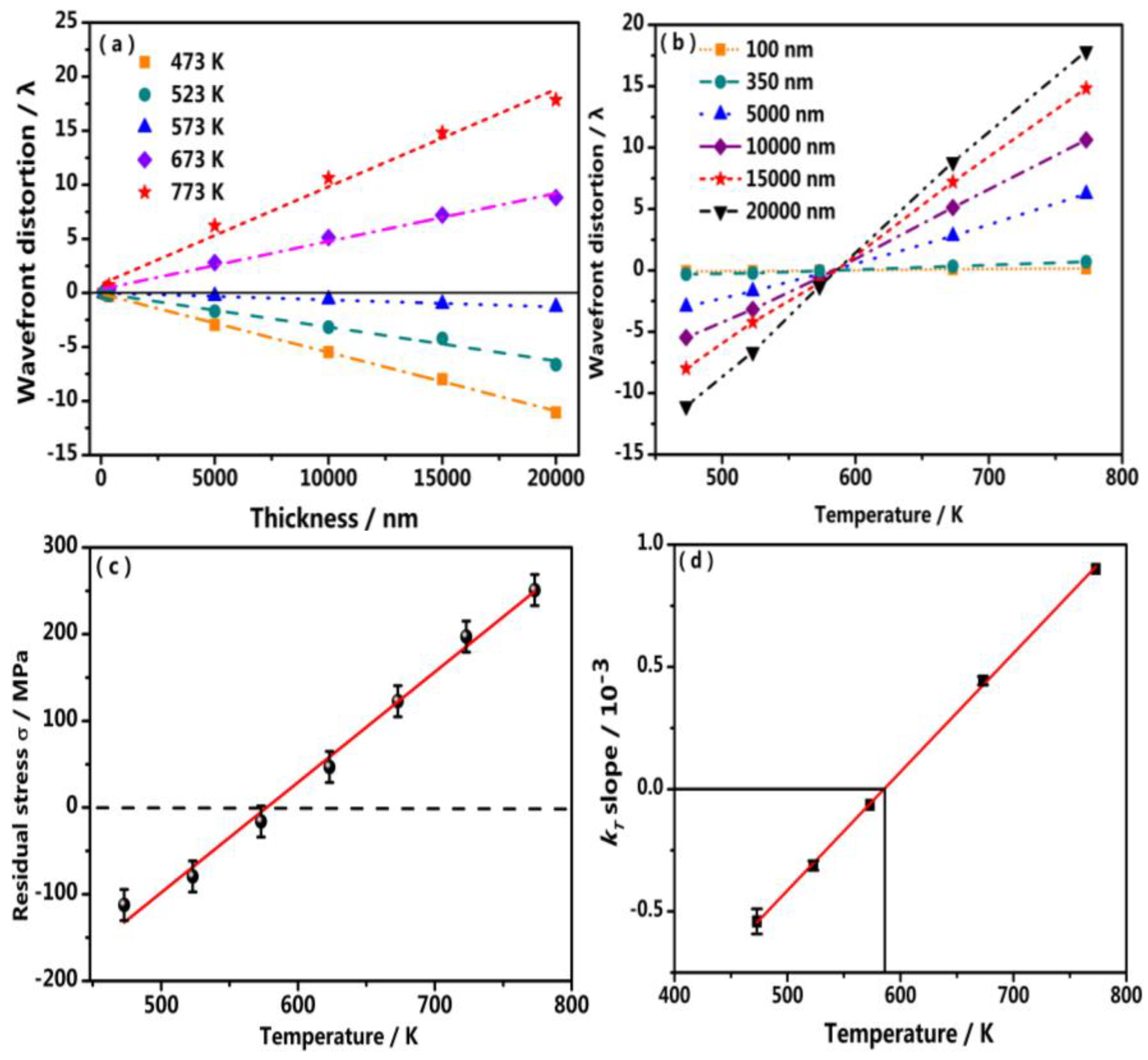
| Annealing Temperature/K | /10−4 | /10−3 |
|---|---|---|
| 473 | −5.4 | −91.9 |
| 523 | −3.1 | −38.8 |
| 573 | −0.7 | −0.7 |
| 673 | 4.4 | 335.2 |
| 773 | 9.0 | 829.5 |
© 2018 by the authors. Licensee MDPI, Basel, Switzerland. This article is an open access article distributed under the terms and conditions of the Creative Commons Attribution (CC BY) license (http://creativecommons.org/licenses/by/4.0/).
Share and Cite
Lv, Q.; Huang, M.; Zhang, S.; Deng, S.; Gong, F.; Wang, F.; Pan, Y.; Li, G.; Jin, Y. Effects of Annealing on Residual Stress in Ta2O5 Films Deposited by Dual Ion Beam Sputtering. Coatings 2018, 8, 150. https://doi.org/10.3390/coatings8040150
Lv Q, Huang M, Zhang S, Deng S, Gong F, Wang F, Pan Y, Li G, Jin Y. Effects of Annealing on Residual Stress in Ta2O5 Films Deposited by Dual Ion Beam Sputtering. Coatings. 2018; 8(4):150. https://doi.org/10.3390/coatings8040150
Chicago/Turabian StyleLv, Qipeng, Mingliang Huang, Shaoqian Zhang, Songwen Deng, Faquan Gong, Feng Wang, Yanwei Pan, Gang Li, and Yuqi Jin. 2018. "Effects of Annealing on Residual Stress in Ta2O5 Films Deposited by Dual Ion Beam Sputtering" Coatings 8, no. 4: 150. https://doi.org/10.3390/coatings8040150
APA StyleLv, Q., Huang, M., Zhang, S., Deng, S., Gong, F., Wang, F., Pan, Y., Li, G., & Jin, Y. (2018). Effects of Annealing on Residual Stress in Ta2O5 Films Deposited by Dual Ion Beam Sputtering. Coatings, 8(4), 150. https://doi.org/10.3390/coatings8040150