3.1. Mechanism for the Emergence of an Electromotive Force during the Heating of ZnO/ZnO–Me Homojunctions without an External Temperature Gradient
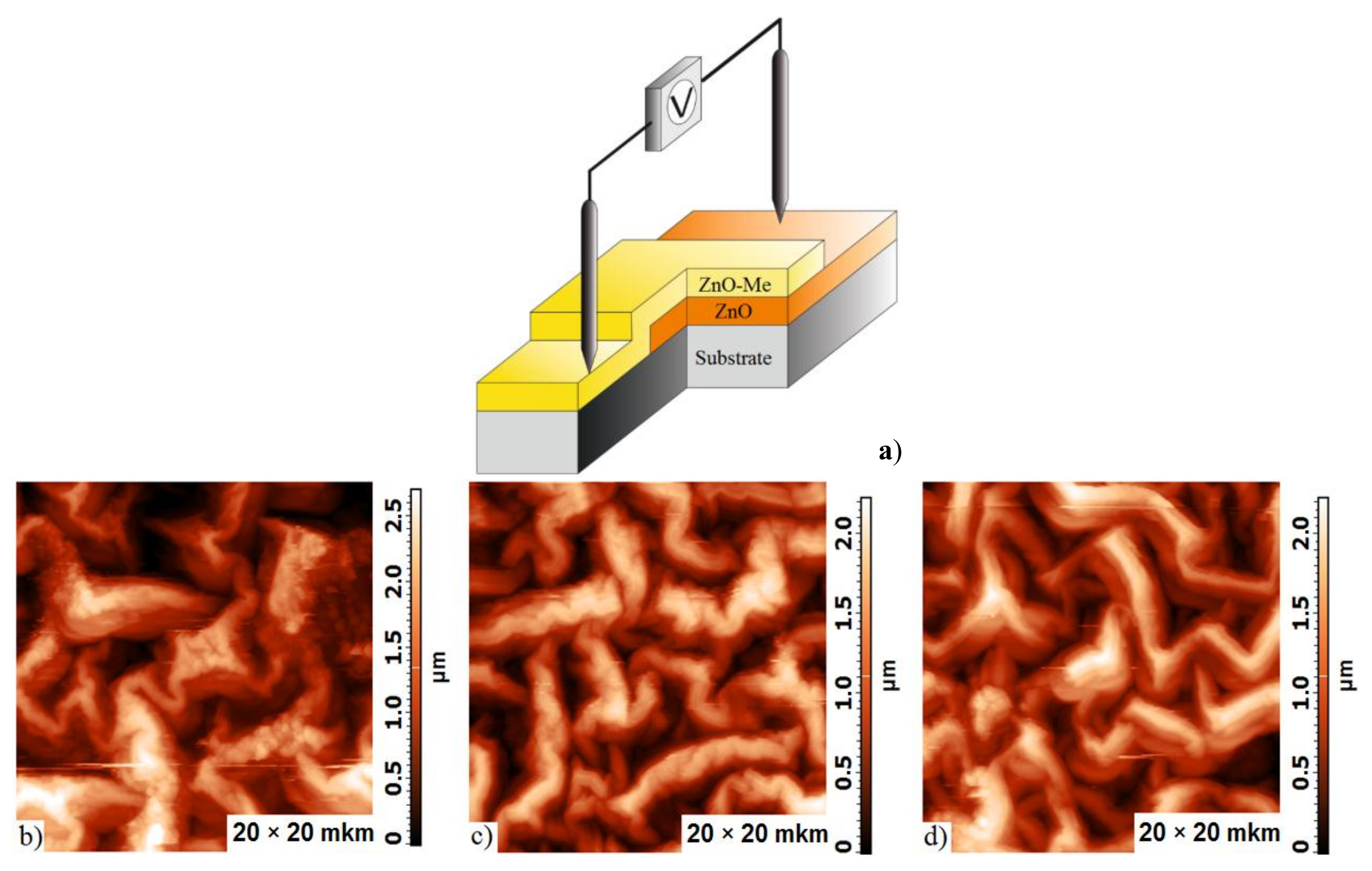
Figure 1b–d shows the structure of the samples studied, as obtained by atomic force microscopy. Image analysis of the surface morphology shows that in all cases the films have a three-dimensional structure with a typical diameter of the branches being 1–2 μm. All of the branches are hierarchically assembled from nanocrystals having a fractal nature and formed during the maturation of the sol.
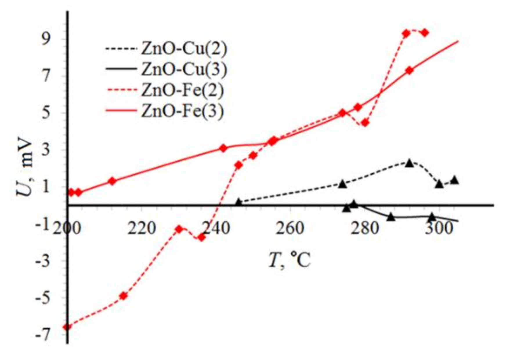
Figure 2 shows the experimental results of the temperature dependence of the electromotive force arising in the samples. We note once again that the samples were heated without a temperature gradient, and before measuring the EMF, temperature control has been carried out for 8 h at each point. After this thermal equilibrium was established, a short circuit of the output electrical contacts, leading to the disappearance of the EMF, occurred. However, after opening the contacts, a complete restoration of the initial electromotive force values was observed. It should also be noted that the obtained values of the EMF were preserved in the “heating-cooling” cycles.
To explain the results obtained, we developed a model based on the “dielectric-conductor” transition in the upper heavily doped ZnO–Me layer. On the one hand, the transition from insulating to metallic systems in semiconductor oxides (for example, ZnO, TiO
2) can be explained by an increase in the concentration of free charge carriers and the formation of a degenerate zone due to doping processes, as suggested by Mott [
14]. However, in the case of high-alloyed semiconductor oxides, where there are both donor impurities and intrinsic electrically active point defects affecting the concentration of free charge carriers, the exact nature of the “insulator-conductor” transition is far from being understood. For example, in [
15], an “insulator-conductor” transition was detected in the ZnO–Ga system for the first time. The authors found that all gallium is in a state Ga
3+ and is an effective donor. However, it was found that an increase in the conductivity of ZnO–Ga thin films is a combined effect, associated both with the presence of gallium impurity and with oxygen vacancies acting as donors. However, pure zinc oxide shows only semiconductor behavior, which indicates the energy of oxygen vacancy levels is controlled by impurities, such as Ga. Thus, the introduction of gallium in ZnO leads to a change in the characteristics of oxygen vacancies and the metallic nature of conductivity. In Reference [
16], an “insulator-metal” transition was observed in the ZnO–Fe system. The authors found that iron is in the zinc oxide matrix in two states, Fe
2+ and Fe
3+. It was shown that the main contribution to the metallic nature of the films is made by the ionization of Fe
3+ state, replacing zinc cations in the crystal lattice. However, in the paper it was noted that the material may also have other sources of free charge carriers, for example, oxygen vacancies and interstitial zinc, which complement the effect of Fe
3+. In the paper [
17], the “insulator-metal” transition in thin ZnO–Nb films was investigated. The authors found that niobium is in a donor Nb
5+ state in the position of zinc cations in the material. The films containing 0.41 at.% Nb showed metallic behavior at ambient temperature. The authors associated it with the formation of a degenerate zone arising from a high level of doping in the framework of the Mott model.
According to X-ray absorption spectroscopy, there is Cu
+ (main), Cu
2+ and Fe
3+ (main), Fe
2+ states, respectively, in ZnO–Cu and ZnO–Fe samples (the details of the zone diagram are presented in [
8]). During the heating of the ZnO/ZnO–Me system, the concentration of charge carriers in the layers will be increased due to both ionization of the main forms of impurities in the material, and the ionization of its own point electrically active defects, first of all, oxygen vacancies, while its value will be larger in the upper layer because of the presence of electrically active impurities. At low temperatures, Coulomb forces retain an electron that is located on the Fe
2+ ion, as well as a hole in Cu
2+, and the main states undergo ionization. However, as the temperature increases, the carrier concentration can reach a critical level when they can screen the ion charge (the Debye screening radius decreases to the Bohr radius of the impurity). In this case, a collective abrupt endothermic process of ionization of the minority impurity forms takes place [
18]. A literature review shows that the collective change in the valence of transition-element cations in zinc oxide with the release of free electrons (for example, Fe
2+ → Fe
3+ + e
−; Mn
2+ → Mn
3+ + e
−, etc.) is well known. For example, in the paper [
19], collective transition processes of iron, manganese, and nickel bivalent cations to trivalent ones, when heated, are shown. It was found that the temperature of release depends both on the type of impurity, and on other features of the material (impurity concentration, surface structure and volume, etc.). In the studied samples, a collective transition Fe
2+ → Fe
3+ + e
– occurred at low temperatures (90–120 K), and the transition Mn
2+ → Mn
3+ + e
− occurred at room temperature. It should be noted that we investigated the ZnO/ZnO–Ga system for the occurrence of a thermovoltaic effect; however, we did not find it. We believe this is due to the fact that gallium is in a single Ga
3+ state in the material.
To be certain, let us discuss the ZnO–Fe semiconductor (all the conclusions are valid for acceptor semiconductors). The initial increase in the electron concentration is mainly determined only by the ionization of iron ions Fe
3+ and oxygen vacancies. Following the authors [
16], we will assume that their contribution is not decisive; therefore, we neglect them in the framework of our quantitative model. Nevertheless, it should be understood that the influence of the own point electrically active defects will introduce an error in the simulation results, which will be discussed in further sections. Thus, the quantity Δ
n1 can be defined as such a concentration, which was formed in a semiconductor due to heating in the temperature range
Tcool–
Tcr. When the temperature reaches
Tcr, there is an abrupt increase in the electron concentration by an amount of Δ
n2 due to the ionization of Fe
2+ form. In this case, we can approximately assume that:
This time dependence of the carrier concentration will affect the appearance of the potential difference, since the sample is non-uniformly doped with mixed-valence impurities. The following effects can occur:
In the region of the sample, where mixed-valence impurities are contained, an excess local concentration of electrons or holes arises that creates a gradient leading to the generation of an electric current. This process leads to the appearance of an opposing field with a potential difference U.
As ZnO/ZnO–Me samples are n–n+-transition (Me = Fe) or n–p-transition (Me = Cu), then the appearance of additional charge carriers charges n+-area negatively (in case of ZnO/ZnO–Fe), and p-area positively (in case of ZnO/ZnO–Cu). This means that both transitions are in forward bias, which is equivalent to applying direct voltage. Thus, some effective value of voltage will be formed on the sample, which is removed by a voltmeter.
To increase the reliability of the developed physical mechanisms, we consider quantitatively the occurrence of the thermovoltaic effect in ZnO/ZnO–Fe and ZnO/ZnO–Cu systems. First, let us analyze the possibility of the occurrence of an isostructural semiconductor-metal phase transition in the ZnO–Fe system.
Iron ions form a solid substitutional solution in zinc oxide, displacing zinc cations into the interstices. According to X-ray absorption spectroscopy, zinc oxide coexists with Fe
2+ and Fe
3+ states in the ratio of 3:7, i.e., Fe
3+ state is preferential [
20]. Ions of Fe
3+ are a donor impurity with ionization energy of ~400 meV, and the energy level of Fe
2+ is located near the Fermi energy of the semiconductor. When a high concentration of donor impurity is introduced into the semiconductor, it is possible to obtain large concentrations of charge carriers that can screen the core charge of impurity atoms, which will facilitate a collective transition of electrons from the level of Fe
2+:
where Δ
Q’ is the heat absorbed during the transition. This process is possible in the case when the Debye shielding radius
rS becomes less than the Bohr radius
rB of electron localization:
For convenience, all of the parameters that will be used in this article are summarized in
Table 1.
The Debye shielding radius is found from the relation [
21]
Considering Equation (3) and
then the condition for the appearance of a transition “insulator-metal” in a semiconductor can be written as:
To calculate the chemical potential ζ
n, it is necessary to take into account the high concentration of impurities in the resulting film ZnO–Fe (3 at.% Fe—1.2 × 10
21 cm
−3), which leads to a difference in the electron energy distribution from the Maxwell-Boltzmann distribution, being a particular case of Fermi-Dirac statistics. Therefore, we will find ζ
n by a numerical method using the electroneutrality equation. To do this, we will make a number of approximations: the concentration of intrinsic electrically active donor defects will be assumed to be negligibly small in comparison with the donor impurity concentration; we will neglect the minority charge carriers; we will only consider electronic transitions from the donor level to the semiconductor conduction band. In this case, the electroneutrality equation can be written as:
. Then, the electron concentration can be written in the following form:
where
is the effective density of states in the conduction band of a semiconductor;
is the Fermi-Dirac integral with an index of 1/2 [
21]. Taking into account that the concentration of ionized donors can be found from the expression [
21]
the calculation of the temperature dependence of the chemical potential is reduced to a numerical solution of the integral equation:
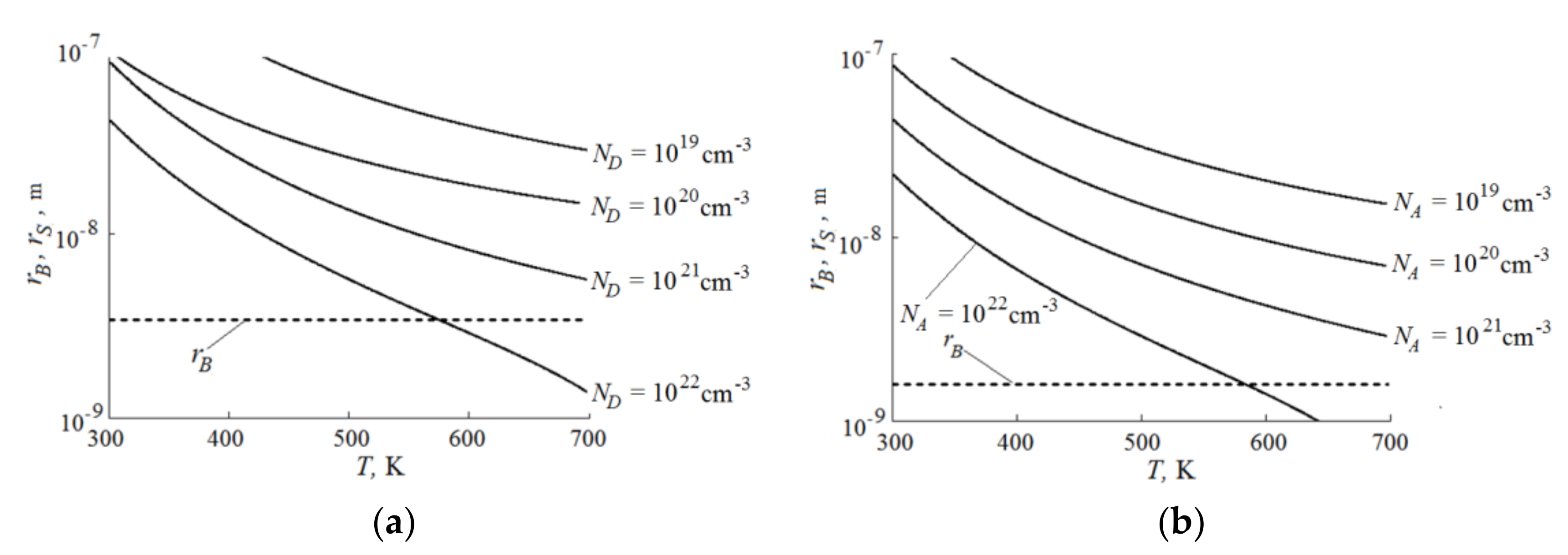
On the basis of the arguments obtained, we calculate the dependence of the Debye shielding radius in the ZnO–Fe system on the temperature for different values of donor impurity concentrations.
Figure 3, illustrates the obtained dependences. The analysis shows that, in the investigated temperature range, in this system the transition “insulator-metal” only occurs at very high impurity concentrations. Thus, when
ND = 10
22 cm
−3, the transition temperature will be 573 K, and at lower concentrations, the temperature will exceed 700 K. The threshold electron concentration required for the transition is ~10
−19 cm
−3. Nevertheless, the obtained electron concentrations necessary for the phase transition are some average values. As in any disordered system, there are impurity fluctuations that determine the deviation from this mean value. This means that at first the transition occurs in local regions that are characterized by the maximum concentration at temperatures lower than those corresponding to the transition “insulator-metal” for averaged concentrations. Apparently, these processes explain the occurrence of the thermovoltaic effect in the ZnO–Fe system at temperatures lower than the calculated ones. With increasing temperature, the dimensions of these regions will grow and lead to the formation of a percolating spanning cluster, when the phase transition covers the entire volume of the material. Also, the contribution to the difference between theoretical and experimental values of the critical temperatures at which the generation of the electromotive force begins is made by other factors that were not taken into account in our quantitative model. First of all, it is the presence of its own electrically active defects in zinc oxide, namely, vacancies in the oxygen sublattice, which act as donors. Their ionization during heating of the system leads to the appearance of a critical concentration of electrons at temperatures that are lower than the calculated ones. It should also be understood that the films are not a single-crystal ZnO sample, but a branched polycrystalline fractal structure actively interacting with the environment. The interaction process leads to the appearance of chemisorbed forms of negatively charged oxygen, the presence of which forms depleted layers on the surface of an
n-type semiconductor. Nevertheless, the obtained values of the critical temperatures at which the generation of the electromotive force occurs, even within such simple approximations, coincide in order with the experimental data, which confirms the value of the developed concepts.
Let us now consider the possibility of the occurrence of an isostructural semiconductor-metal phase transition in the ZnO–Cu system. Copper is an acceptor impurity in zinc oxide. When a solid substitutional solution is formed, copper Cu
+ cations displace Zn
2+ into interstices and act as acceptors with ionization energy of 369 meV. A small number of Cu
+ cations occupy positions in the interstices of the crystal lattice, playing the role of donor impurities with activation energy of 109 meV. The Cu
2+ state is 200 meV lower the bottom energy of the conduction band [
22].
Carrying out a simulation that is similar to the ZnO–Fe system, we obtain the results that are presented in
Figure 3b. It can be seen that the obtained dependences are analogous to ZnO–Fe. Nevertheless, an important feature of the results should be noted. Since the activation energies of Fe and Cu impurity atoms are practically the same, the main contribution to system differences is made by the difference in the effective masses of electrons and holes in zinc oxide. Since the effective mass of holes in zinc oxide is greater than the effective mass of an electron, an increase in the concentration of free charge carriers with increasing temperature is faster. It should be expected that the transition “insulator-metal” in the system would occur at lower temperatures than for the ZnO–Fe system, where the main carriers are electrons. However, for the concentration of the acceptor impurity of 10
22 cm
−3, the transition occurs at 584 K, which is higher than for ZnO–Fe at the same donor concentration. This is due to the decrease in the Bohr radius in ZnO–Cu related to the higher effective mass of holes in ZnO.
Thus, the calculation of the temperature of the occurrence of the thermovoltaic effect within the framework of the developed simple physical mechanisms in ZnO–Cu and ZnO–Fe systems describes the experimental results obtained quite well. Firstly, it is shown that in the ZnO–Cu system the critical temperature of the electric voltage generation will be higher than in the ZnO–Fe system. Secondly, the obtained absolute temperature values are close to the experimental values (especially for the ZnO–Cu system). The reasons for the lower temperatures of the beginning of generation in comparison with the calculated ones are considered above.
A logical development of the proposed model will be taking into account the effect of the own point electrically active defects in the material on the values of the critical temperature at which the “insulator-metal” transition occurs. However, it should be noted that this is not an easy task. As it was shown in [
15], the total concentration of free charge carriers is not an additive sum of ionized forms of impurities and defects, and there is an effect of external doping on the ionization efficiency of oxygen vacancies. In the first approximation, when developing a more accurate model, one can use ideas about the change in number of ionized point defects when the Fermi level changes position in a semiconductor. Defective states in zinc oxide have several levels in the forbidden zone [
23]. Therefore, the predominant form of the charge will be determined by the position of the Fermi level, which depends on the doping level of the semiconductor. It should also be noted the possibility of the formation of clusters of charged defect and impurity states in the semiconductor. At the same time, at some annealing temperatures, oppositely charged defects diffuse to each other, forming clusters, which significantly affect the electrophysical properties of the material, including the energy of the defect states themselves. The development of these physical mechanisms is the subject of our further research.
3.2. Development of Physical Mechanisms of Temperature Dependence of the Electromotive Force Arising in Zn/ZnO–Me Homojunctions
Let us analyze the experimentally obtained dependences in
Figure 2, while taking into account the possibility of oxygen chemisorption on the surface of the films, as well as the mutual transition of various forms of chemisorbed oxygen with a change in temperature.
The EMF temperature dependence will increase linearly in the 200–300 °C range from 0 to 10 mV for ZnO/ZnO–Fe samples, the upper layer of which is formed by three immersions. This dependence can be explained in the following way: in the semiconductor, as in any other disordered system, there are fluctuations in the impurity concentration characterizing the deviation from the mean value. At low temperatures, the semiconductor-metal transition will occur only in the local parts of the sample with the maximum value of the concentration of free electrons. As the temperature rises, the region of existence of the phase transition will grow, which is equivalent to an increase in the negative potential in the ZnO–Fe region. Thus, an increase in temperature will lead to an increase in the electromotive force arising in homojunctions.
It can be seen from
Figure 2 that the samples of ZnO/ZnO–Fe, the upper layer of which is formed by two immersions, behave somewhat differently. The features of this series of samples include a change in the sign of the polarity of the emerging EMF, as well as a large deviation of its temperature dependence on the linear function.
The first feature, apparently, can be explained by a combination of various factors, the main of which are:
Emergence of a potential barrier under point contact and the possibility of an inversion layer. In this case, the system becomes n–n+–p, and in a certain temperature range the polarity of the EMF taken will be different. With increasing temperature due to ionization of the donor impurity, the inversion layer will decrease and disappear at some critical value. With further temperature growth, the U(T) dependence will be close to the same dependence as for a series of samples, the upper layer of which is formed by three immersions;
Probability of emergence of piezo-, flexo- and pyroelectric effects in zinc oxide films;
Emergence of new phases on the surface of films (for example, copper and iron oxides), which can lead to the appearance of depleted, enriched or inversion layers at interfaces.
Nevertheless, despite a large number of factors capable of influencing the polarity and magnitude of the electromotive force arising in the samples, it should be understood that its very appearance cannot be explained by these effects. The fact is that pyro-, piezo-, flexoelectric, and other effects can occur in our samples during heating. However, after the establishment of thermal equilibrium at a given temperature, the resulting EMF should exponentially decay. In addition, we have short-circuited the output contacts, which should lead to the EMF relaxation. However, further measurements showed the restoration of the original value of the EMF. On the basis of these data, it can be concluded that the very appearance of the electromotive force in samples is only explained by the “dielectric-metal” transition. It should also be noted that when developing a model of the dependence of the output voltage on temperature, it is necessary to take into account the formation of p–n and n–n+ junctions in our materials. However, this is beyond the scope of our work, since our model calculates only the critical temperature in the alloyed film, at which the “dielectric-metal” transition occurs, leading to the appearance of the EMF.
As it was shown earlier, the surface of the film formed by two immersions is more developed than the surface formed by three immersions for both ZnO–Fe and ZnO–Cu samples. On the basis of this, it can be assumed that the chemisorbed forms of oxygen will exert a stronger influence on the electrophysical properties of the samples in the first case.
Oxygen, being an oxidizing gas, will carry out the capture of free electrons from the semiconductor, which will eventually lead to a decrease in the value of the electromotive force due to the thermovoltaic effect. There are two characteristic breaks at temperatures of ~240 and 280 °C on the
U(T) dependence for the ZnO/ZnO–Fe samples, the upper layer of which is formed by two immersions. Apparently, their appearance corresponds to the processes of mutual transitions of various forms of chemisorbed oxygen, which can be accompanied by a sharp increase or a decrease in the concentration of free electrons in the semiconductor, manifested in a narrow temperature range [
24]. It is likely that the main contribution to the presented dependences is made by the following processes [
25,
26]:
The EMF temperature dependences for ZnO/ZnO–Cu samples are, in fact, analogous to the same dependences for ZnO/ZnO–Fe samples. It is established that the semiconductor-metal transition in ZnO–Cu system will occur at higher temperatures than in the analogous ZnO–Fe system: the onset of EMF generation for ZnO/ZnO–Cu samples occurs at a higher temperature than for the ZnO/ZnO–Fe samples.
The
U(T) dependence for ZnO/ZnO–Cu samples, the upper layer of which is formed by three immersions, is close to linear. It should be noted that with the same configuration of the voltmeter contacts that was used in the ZnO/ZnO–Fe system, the EMF value will have the opposite sign, since ZnO/ZnO–Cu samples are of
n–p+ structure, as shown in
Figure 1.
The temperature dependence for ZnO/ZnO–Cu samples, the upper layer of which is formed by two immersions, changes the EMF sign. Apparently, this process can also be associated with phenomena under point contact, accompanied by the emergence of potential barriers and an inversion layer. A significant deviation of the dependence on the linear form at temperatures of 290–300 °C both for a given series of samples and for ZnO/ZnO–Fe samples can be due to mutual transitions of various forms of chemisorbed oxygen.
The approaches that were developed in this work can be useful for explaining the thermovoltaic effect in a wide range of materials, for example, in germanium-silicon films heavily doped with titanium [
27], variable-gap solid solutions of Si
xGe
1−x [
11], in which this effect has been detected in recent years.


