Article

CuO and CuO/Graphene Nanostructured Thin Films as Counter Electrodes for Pt-Free Dye-Sensitized Solar Cells

Department of Opto-Electronic Engineering, National Dong Hwa University, Hualien 97401, Taiwan
*
Author to whom correspondence should be addressed.
Coatings 2018, 8(1), 21; https://doi.org/10.3390/coatings8010021
Submission received: 20 November 2017 / Revised: 24 December 2017 / Accepted: 30 December 2017 / Published: 3 January 2018
(This article belongs to the Special Issue Functional Oxide and Oxynitride Coatings)

Abstract

:
Copper oxide (CuO) and CuO/graphene nanostructured thin films were used as counter electrodes (CEs) for dye-sensitized solar cells (DSSCs). CuO and CuO/graphene pastes were prepared and coated on fluorine-doped tin oxide (FTO) glass substrates using a doctor-blade coating method. The substrates were then sintered at 350 °C for 30 min to form CuO and CuO/graphene nanostructures. The material properties of the CuO and CuO/graphene CEs were analyzed using a scanning electron microscope, transmission electron microscope, energy-dispersive spectrometer, thermogravimetric analysis instrument, X-ray diffractometer, Raman spectroscopy, X-ray photoelectron spectrometer, ultraviolet-visible spectrophotometer, and cyclic voltammetry instrument. The CuO and CuO/graphene CEs were used to fabricate DSSCs, and the device characteristics were analyzed using current density–voltage, incident photo-to-current conversion efficiency, and electrochemical impedance spectroscopy measurements. The results showed that when CuO and CuO/graphene were used as the CEs, the device conversion efficiencies were 2.73% and 3.40%, respectively. CuO is a favorable replacement for expensive platinum (Pt) because it features a simple fabrication process and is inexpensive and abundant. Furthermore, graphene, which exhibits high carrier mobility, may be added to enhance the electrical and catalytic abilities of CuO/graphene CEs. This is the first study to examine the use of CuO and CuO/graphene for developing Pt-free CEs in DSSCs.

1. Introduction

Energy shortages and environmental pollution are two major problems for humans this century. Considerable research and development of alternative and renewable energies as substitutes for conventional energy sources has been conducted in recent years. Of the renewable energy sources, solar energy is one of the most advantageous because it is inexhaustible and is environmentally friendly [1]. In 1991, Grätzel et al. [2] developed a new type of solar cell, namely the dye-sensitized solar cell (DSSC), based on the high-surface-area TiO2 nanoparticles. DSSCs feature the advantages of high efficiency, low cost, and simple fabrication, which make them a strong potential competitor for conventional silicon-based solar cells [3,4,5,6,7,8,9,10,11,12]. Structurally, DSSCs contain TiO2, dyes, and electrolytes in addition to platinum (Pt) counter electrodes (CEs), which play the critical role of catalyzing iodide ions in redox reactions [13]. However, Pt CEs are expensive; hence, seeking an alternative to such electrodes to reduce fabrication costs has become a prominent research topic [14,15]. According to the literature, materials that can be used for making DSSC CEs include graphite, carbon nanotubes, graphene, conductive polymers, and metal oxide semiconductors [16,17,18,19,20,21,22,23].
Copper oxide (CuO) is a slightly water-absorbing black oxide of copper with a relative molecular mass of 79.545, a density of 6.3–6.9 g·cm−3, and a melting point of 1326 °C. In addition, CuO is a p-type semiconductor having an energy gap width of approximately 1.2 eV. CuO is a secondary copper mineral, which is the most stable form of oxidized copper. It has a monoclinic structure and many remarkable properties such as superconductivity, catalytic activity, optoelectronic properties, high stability, and antibacterial activity. CuO can be used to fabricate various high-performance electronic and optoelectronic devices such as high-temperature superconductors, gas detectors, and giant magnetoresistive devices [24,25]. CuO can be fabricated using numerous methods including sonochemical, microwave irradiation, hydrothermal, precursor thermal decomposition, and electrochemical approaches [26,27,28]. Since CuO fabrication is easy, the number of studies using CuO to fabricate solar cells has increased in recent years. Habibi et al. fabricated DSSC working electrodes by depositing CuO–ZnO thin films using a hydrothermal process and combined cobalt electrolytes with Pt CEs; their device demonstrated an efficiency of 0.01%–0.03%, which, although inadequate, showed considerable potential for improvement [29].
Graphene, a new carbon material, has been extensively applied in recent years. Graphene has become the focus of recent research because of its unique properties such as high mechanical strength (1100 GPa), high thermal conductivity (5000 W·m−1·K−1), and high carrier mobility (200,000 cm2·V−1·s−1) [30,31]. Some researchers have recently applied graphene to the preparation of DSSC devices [32,33,34]. Zhang et al. [35] scattered graphene nanosheets (GNs) in a terpineol and ethyl cellulose ethoce solution, coated the GNs on the surface of fluorine-doped tin oxide (FTO) glass plates, and examined the effect of annealing temperature on the performance of DSSC devices. The results showed that the GN CE obtained at an annealing temperature of 450 °C achieved the highest conversion efficiency of 2.94% for DSSCs. Roy-Mayhew et al. [36] used functionalized graphene sheets as DSSC CEs. Using cyclic voltammetry (CV) measurements, they found that the addition of oxygen-containing functional groups increase the surface catalytic activity of graphene.
CuO has been extensively investigated for photovoltaic and photoelectrochemical proton reduction applications. Two valuable advantages of using CuO are that it is nontoxic and its constituents are abundantly available. The work function of CuO is approximately 5.3 eV, which is appropriate for use as a CE in DSSCs. In this study, CuO and CuO/graphene nanostructures were fabricated as CEs for DSSCs. The electrode properties of CuO and CuO/graphene CEs were comprehensively analyzed, and the effects of CuO and CuO/graphene CEs on the performance of DSSCs were investigated.

2. Experimental

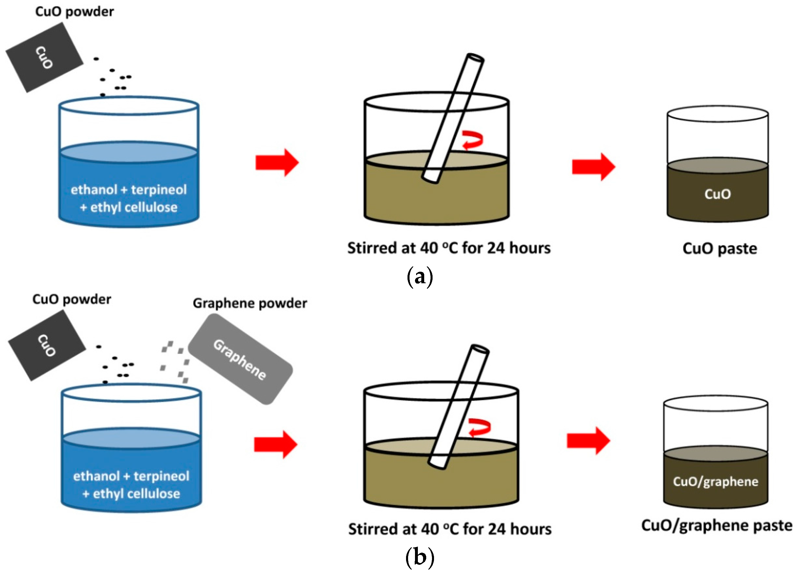
2.1. Preparation of the CuO and CuO/Graphene Pastes

CuO and CuO/graphene pastes were prepared to fabricate CuO and CuO/graphene CEs. Figure 1 shows the process of preparing the CuO and CuO/graphene pastes. The CuO nanopowders/nanoparticles (CuO, 99%, 80 nm in diameter) were purchased from a commercial source (US Research Nanomaterials, Inc., Houston, TX, USA). First, to prepare an ethyl cellulose solution, 10 wt % ethyl cellulose powder was added to 90 wt % ethanol and stirred at room temperature for 48 h using a magnetic stirrer. Next, 20 wt % CuO nanoparticles (approximately 80 nm in diameter), 70 wt % terpineol, and 10 wt % ethanol were added to the ethyl cellulose solution; the mixture was stirred at 40 °C for 24 h using a magnetic stirrer. Subsequently, the paste bottle was left standing for the remaining ethanol to volatilize, and a viscous CuO paste was formed. Concurrently, a CuO/graphene paste was prepared to fabricate the CuO/graphene electrodes. The GNs (graphene P-MF10) were purchased from a commercial source (Enerage Inc., Yilan County, Taiwan). To prepare the CuO/graphene paste, an ethyl cellulose solution with 10 wt % ethyl cellulose powder was supplemented with 18 wt % CuO nanoparticles (approximately 80 nm in diameter), 2 wt % GNs, 70 wt % terpineol, and 10 wt % ethanol; similarly, the mixture was stirred at 40 °C for 24 h using a magnetic stirrer. Finally, the paste bottle was left standing for the remaining ethanol to volatilize, thereby forming a viscous CuO/graphene paste. The GO/graphene paste had a CuO-to-graphene weight ratio of 9:1.

2.2. Preparation of the Counter Electrodes

Figure 2 shows the schematic device structure of a DSSC fabricated using a CuO or CuO/graphene CE. To fabricate CEs, the following method was adopted: First, FTO transparent conductive glass substrates were prepared. Two holes were drilled on the transparent conductive glass substrates to be used for injecting electrolytes. Subsequently, the glass substrates were placed in acetone and washed for 10 min using an ultrasonic cleaner. Next, deionized water was added to the cleaner to wash the glass substrates for another 10 min. Ethanol was then added to the cleaner to wash the glass substrates for 10 min. Finally, deionized water was added to the cleaner again to wash the glass substrates for another 10 min, completing the cleaning process of the FTO glass substrates.
The cleaned glass substrates with holes were dried using a nitrogen air gun. The two sides of the glass substrates were taped with a transparent tape, which was evenly pressed to ensure no air bubbles were trapped and to prevent uneven taping on the surface. Next, the CuO and CuO/graphene pastes were coated on the glass substrates using a doctor-blade method, after which the glass substrates were placed inside a furnace to vacuumize them and produce a glass pressure of 7 mTorr. Next, nitrogen was injected into the tube furnace at a rate of 300 cc·min−1. The nitrogen bottle outlet pressure was maintained at a constant value while air and nitrogen were continuously sucked out and injected, separately, for 3 min, creating a nitrogen atmosphere in the tube furnace. Next, the air suction pump was turned off, whereas the nitrogen injection valve was left on until the furnace pressure rose to 300 Torr, after which the nitrogen injection valve was turned off. Finally, the glass substrates underwent high-temperature sintering to 350 °C for 30 min in the nitrogen atmosphere and were left to anneal to room temperature, producing the CEs.

2.3. Analysis of Counter Electrode Characteristics

A complete analysis of various CEs was performed in this study. An electrode surface morphology analysis was conducted using a scanning electron microscope (SEM) (JEOL JSM-7000F, JEOL, Tokyo, Japan). The electrode morphology was observed using a transmission electron microscope (TEM) (JEOL JEM-1400, JEOL, Tokyo, Japan), In addition, an energy-dispersive spectrometer (EDS) (JEOL JSM-7000F) was used to analyze the CE element type and content. The composition of CuO/graphene CEs was investigated through a thermogravimetric analysis (TGA) instrument (SETSYS Evolution TGA-DTA/DSC, SETARAM, Inc., Cranbury, NJ, USA), and a material property analysis was completed using a Raman spectrometer. The crystal structure of various electrodes was also observed using an X-ray diffractometer (XRD) (Rigaku D/Max-2500V, Rigaku, Tokyo, Japan). Furthermore, an X-ray photoelectron spectrometer (XPS) (Thermo K-Alpha, Thermo Fisher Scientific, Waltham, MA, USA) was used to analyze the chemical element composition on the electrode surfaces. The transmittance of the electrodes was characterized using an ultraviolet-visible (UV-VIS) spectrophotometer (OPTIZEN POP UV/VIS spectrophotometer, Mecasys Co., Ltd., Daejeon, Korea), and the electrode catalytic activity was measured using a CV instrument (CH Instruments 6116D, CH Instruments, Inc., Austin, TX, USA).

2.4. Fabricating the Working Electrodes

The cleaned FTO transparent conductive glass substrates were dried using a nitrogen air gun. A piece of transparent tape was drilled with holes measuring 0.126 cm2 and taped onto the glass substrates. The holes were then blade coated with small TiO2 nanoparticles (approximately 25 nm in diameter, anatase phase) (Ti-Nanoxide T/SP, Solaronix SA, Aubonne, Switzerland). Next, the glass substrates were placed on a hot plate and baked at 150 °C for 10 min before being left to cool at room temperature. Subsequently, the substrate was blade coated with large TiO2 nanoparticles (approximately 200 nm in diameter, anatase phase) (Ti-Nanoxide R/SP, Solaronix SA, Aubonne, Switzerland). The original tape was then removed, and the glass substrates were placed inside the furnace to sinter at 500 °C for 30 min before being left to cool at room temperature. Finally, the glass substrates were soaked in a dye solution for 20 h, completing the fabrication of the working electrodes. The dye solution used in this experiment was made by dissolving 0.5 mM N719 dye and 0.5 mM chenodeoxycholic acid in acetonitrile and tert-butyl alcohol at a 1:1 ratio.

2.5. Fabricating the DSSCs

A 60-μm-thick sealing foil was cut into a 2.5 cm × 2.5 cm square. Next, a 0.8 cm × 0.8 cm hole was made in the center of the sealing foil. The sealing foil was then placed between a working electrode and a CE, and the hole of the sealing foil was carefully adjusted before the whole arrangement was placed in an encapsulator and compressed at a temperature of 130 °C and a pressure of 3 kg·cm−2 for 3 min to completely seal the upper and lower electrodes. After the device was left to cool, 5 μL of electrolytic solution was injected into the device using a micropipette. The electrolytic solution consisted of 12.6 mg of I2, 33.5 mg of LiI, 0.36 mL of 4-tert-butylpyridine, and 5 mL of acetonitrile as the electrolyte solvent. Next, the 0.8 cm × 0.8 cm sealing foil and a glass slide were used to quickly seal the device at 130 °C for 10 s to prevent the electrolytic solution from leaking out and volatilizing. Finally, the surface of the glass was wiped clean with alcohol to complete the DSSC device fabrication. The characteristics of the DSSC devices were analyzed through current density–voltage (JV), incident photo-to-current conversion efficiency (IPCE), and electrochemical impedance spectroscopy (EIS) measurements. The complete details of the measurements are described in a report of our previous work [23].

3. Results and Discussion

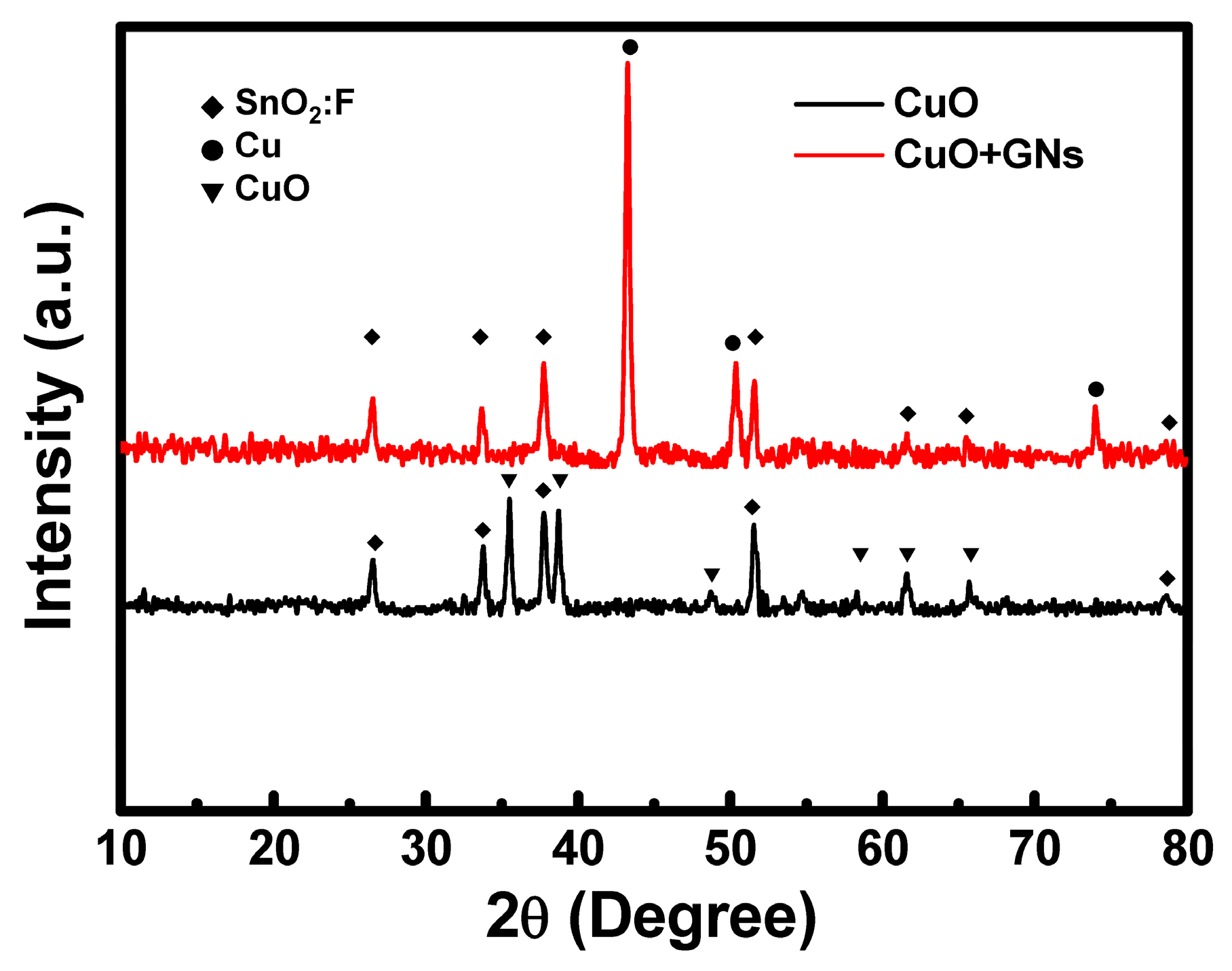
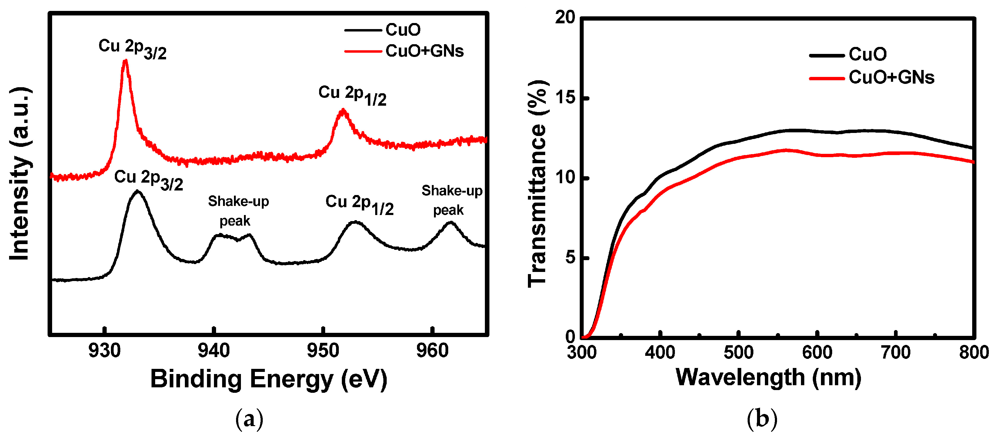
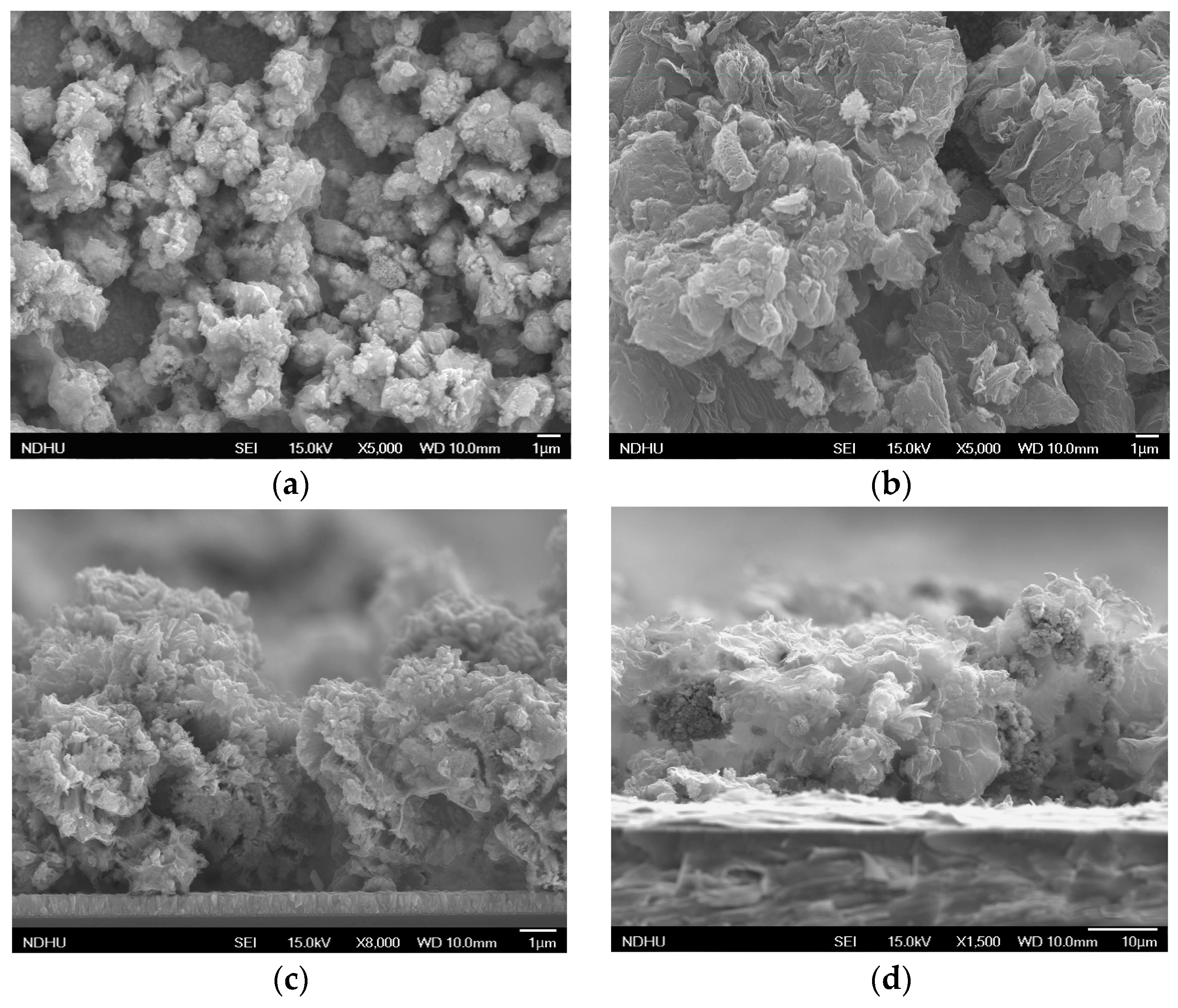
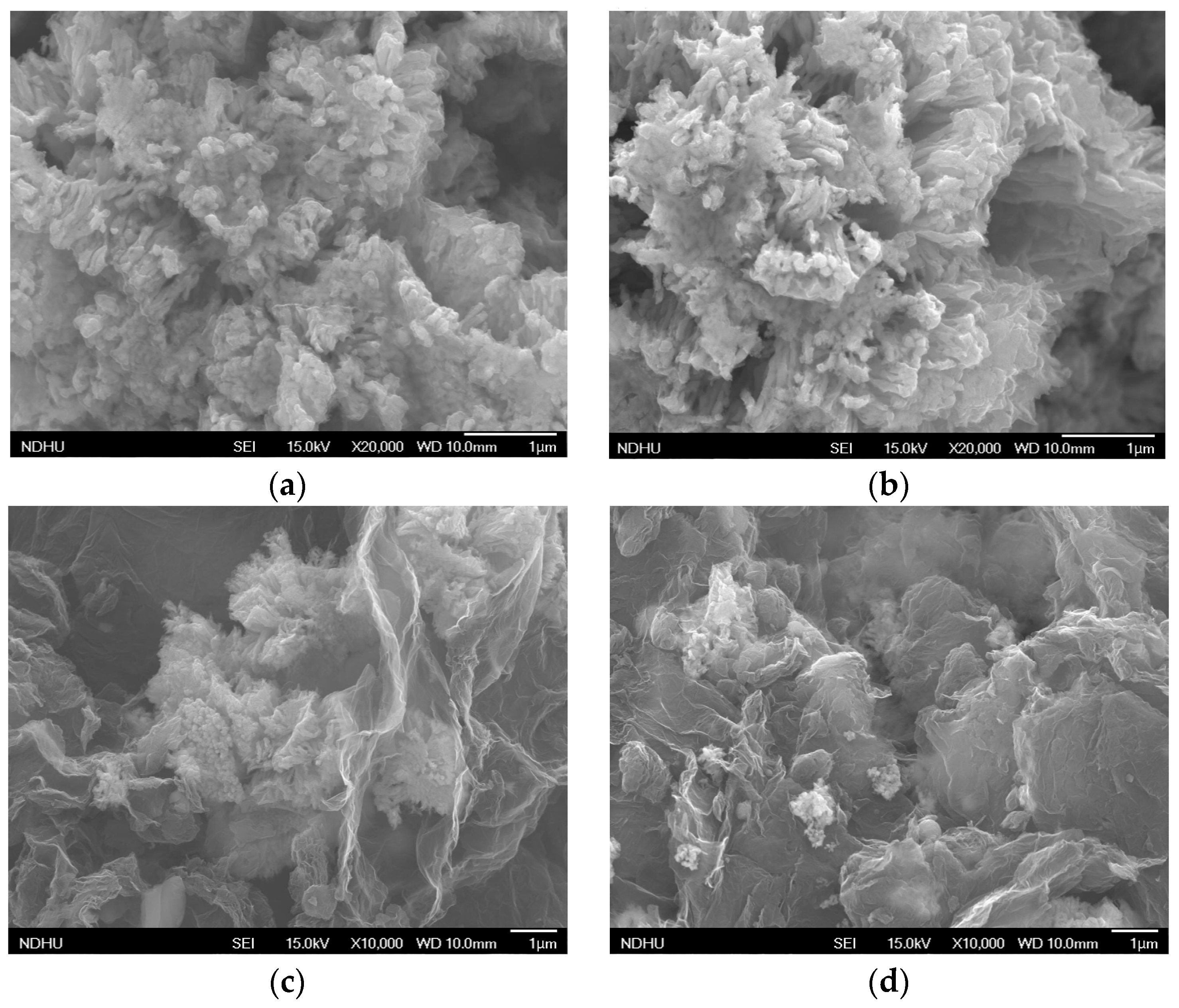
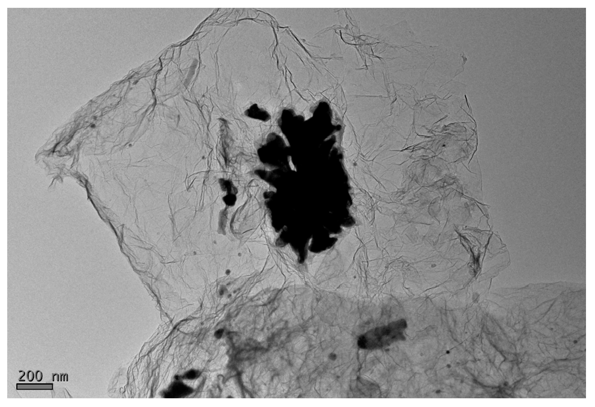
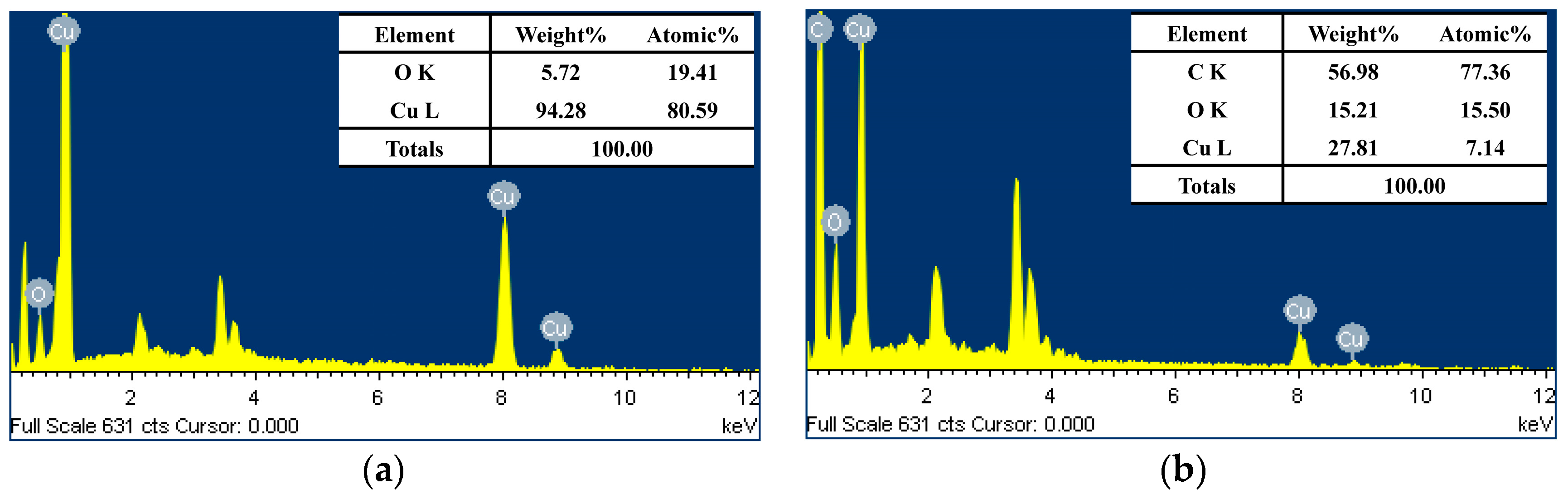
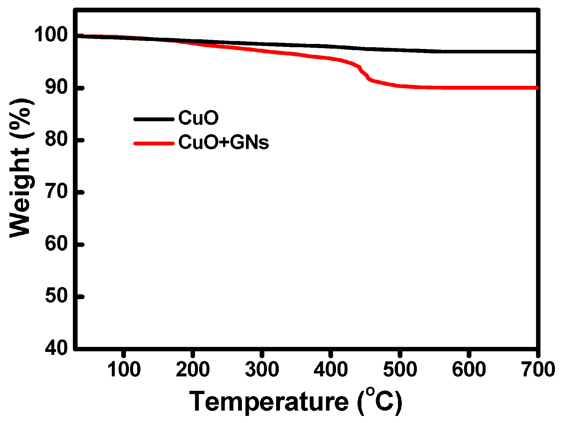
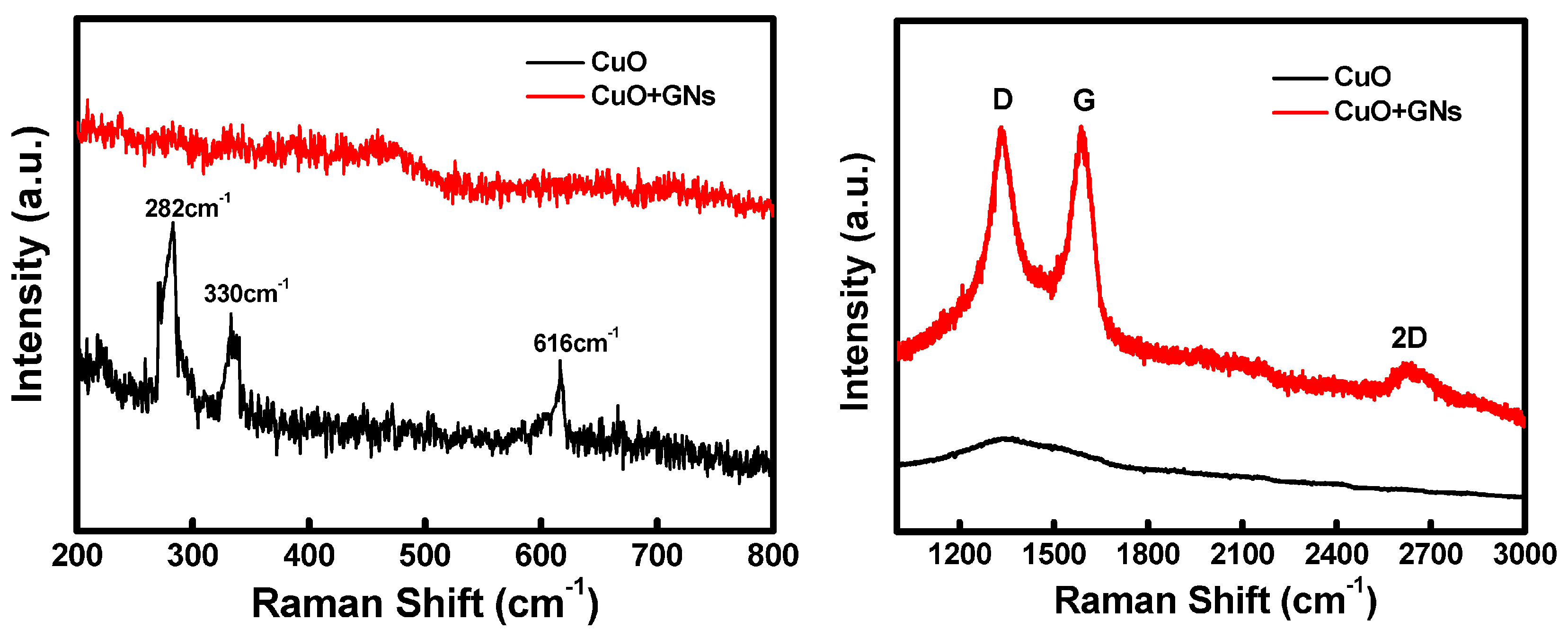
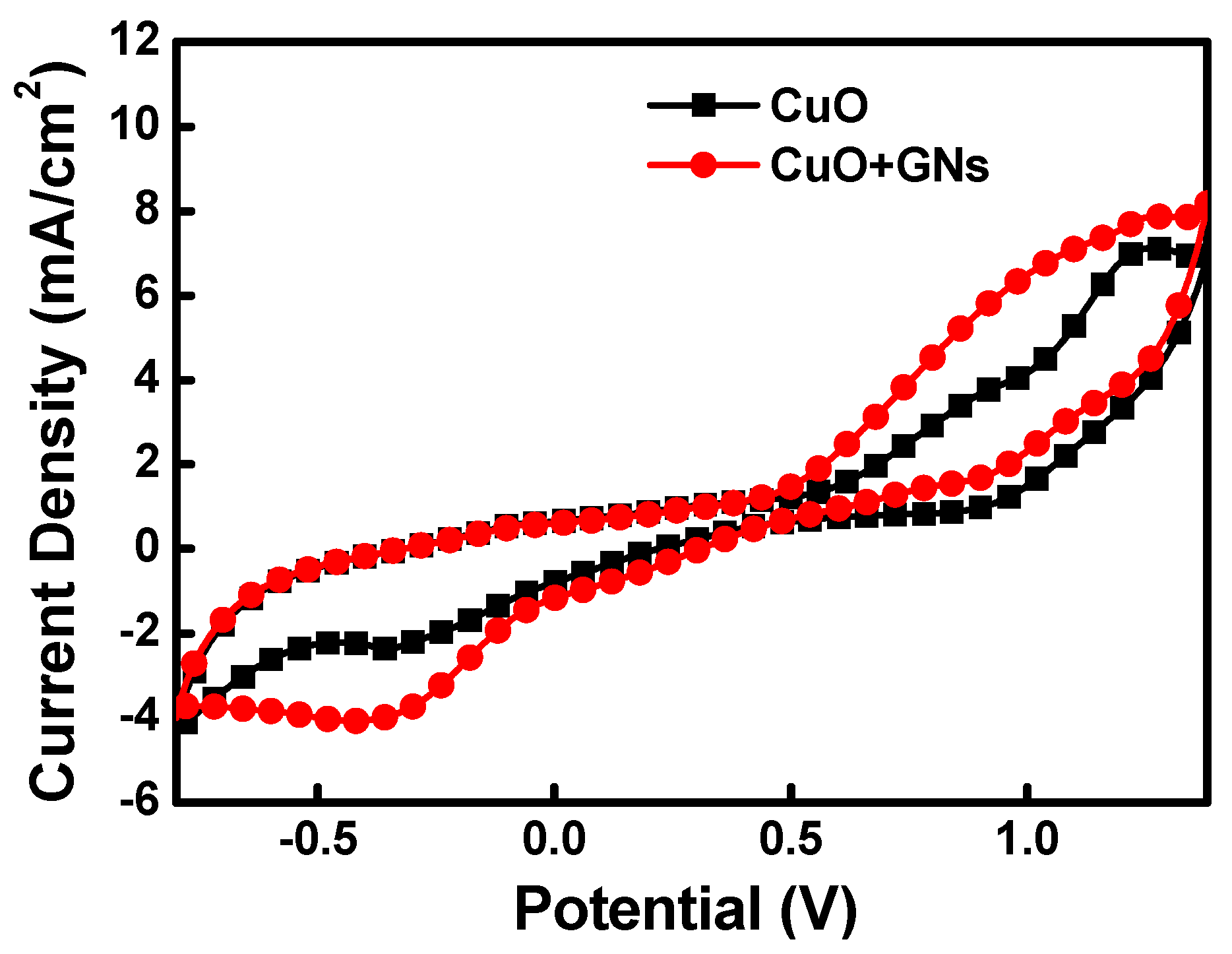
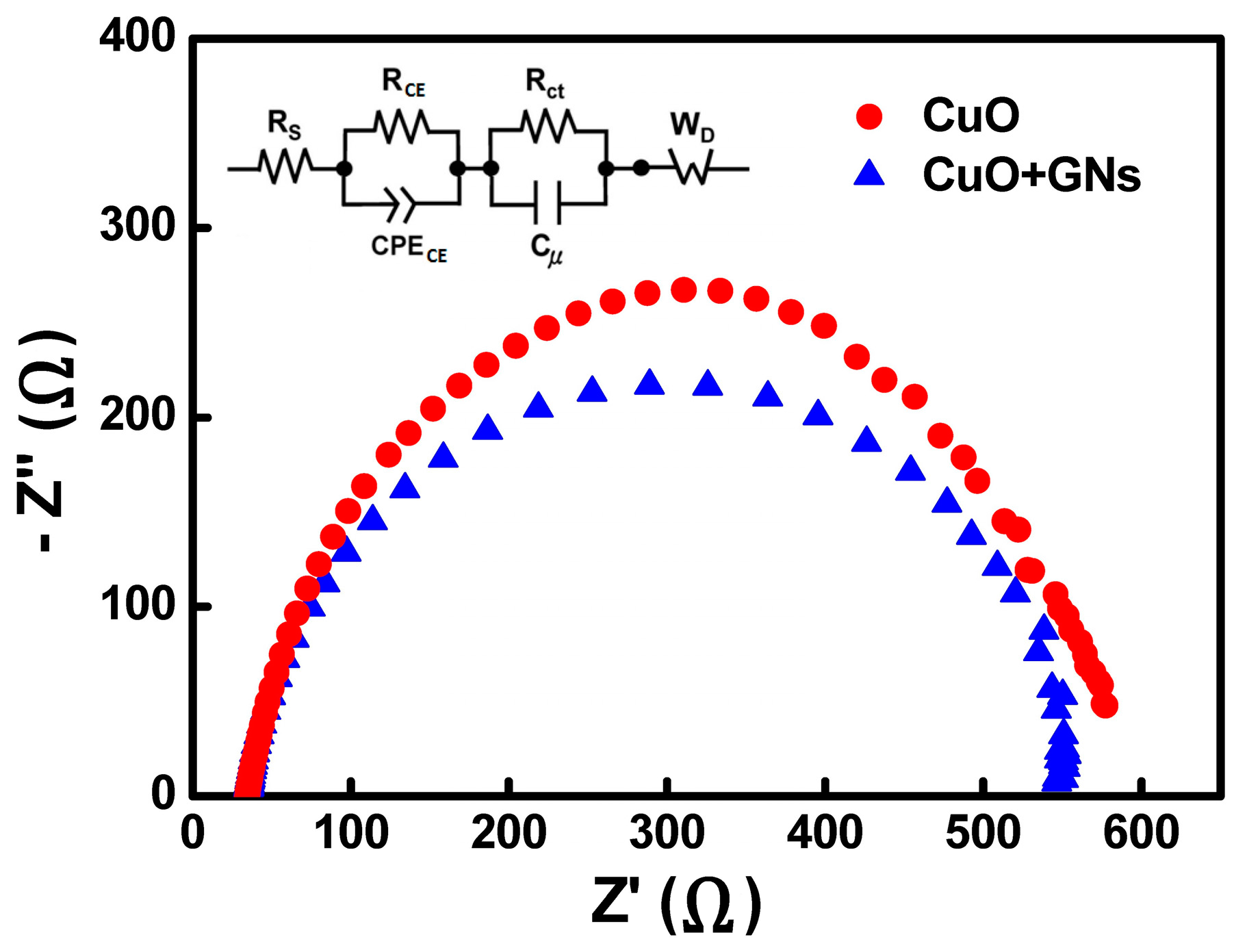
3.1. Characterization of the CuO and CuO/Graphene CEs

Figure 3 shows the top-view and cross-sectional SEM images of CuO and CuO/graphene CEs. As presented in Figure 3a, the CuO CE exhibited a granular structure; the size of the granular structure was approximately 1–4 μm, and the structure was composed of CuO nanoparticles (approximately 80 nm in diameter). The solution pH, ionic strength, and presence of natural organic and inorganic colloids may have modified the surface conditions of the CuO nanoparticles, which caused the aggregation of the CuO nanoparticles. As shown in Figure 3b, the CuO/graphene CE displayed a foliated and granular structure; graphene exhibited a nanosheet structure, whereas CuO had a granular structure. The granular structure was composed of CuO nanoparticles (approximately 80 nm in diameter) and was distributed on the foliated graphene surface. Figure 3c,d depict the cross-sectional SEM images of CuO and CuO/graphene. The thicknesses of the CuO and CuO/graphene nanostructured thin films were 10.5 and 24.1 μm, respectively.
Figure 4a,b show the SEM images of the CuO CEs fabricated with 20 wt % and 30 wt % CuO concentrations, respectively. The SEM result indicated that increasing the CuO concentration engendered an increased number of CuO naoparticles in the granular structures. Figure 4c,d present the CuO/graphene CEs fabricated with CuO:GNs (9:1) and CuO:GNs (8:2) weight ratios in the CuO/graphene pastes. The SEM result indicated that increasing the GNs ratio in CuO/graphene CEs may have affected the surface morphology of the CuO/graphene CEs. As the concentration of the GNs increased, the number of the sheet-like GNs decreased due to the stacking effect of GNs. In addition, the morphology of the CuO/GNs was observed by a TEM (Figure 5). The GNs exhibited a crumpled morphology and a paper-like structure, and the CuO nanoparticles were aggregated and distributed on the GNs.
Figure 6 shows the EDS analysis results of the CuO and CuO/graphene CEs. An EDS was used to analyze the elemental composition and content of the test samples. The EDS analyses of the CuO and CuO/graphene CEs showed that under the sintering condition of 350 °C in a pure nitrogen environment, the weight ratios and atomic numbers of O and Cu in the CuO electrode were 5.72:94.28 and 19.41:80.59, respectively, whereas those of C, O, and Cu in the CuO/graphene electrodes were 56.98:15.21:27.81 and 77.36:15.5:7.14, respectively. The EDS results demonstrated that the C content was significantly increased in the CuO/graphene CEs. In addition, the EDS results showed that the O and Cu content did not fit the stoichiometry of CuO in terms of atomic percentage. This is because EDS cannot be considered a quantitative method of analysis, especially for light elements (i.e., carbon); it can only be used as a qualitative analysis for various elements in an electrode. The composition of the CuO/graphene CEs was further investigated by a TGA instrument under an air atmosphere (Figure 7). CuO nanoparticles had high thermal stability with little or no significant mass loss below 700 °C. The final weight percentage of CuO in the CuO/graphene composite was 88.6 wt %, indicating a weight percent of graphene in the CuO/graphene CE of approximately 11.4 wt %.
Raman spectroscopy involves exciting a test sample using a laser and studying the crystal lattice of the test sample as well as its molecular vibrations and rotational modes using photon–phonon interactions. The Raman spectra of the CuO and CuO/graphene electrodes sintered under a nitrogen atmosphere at a temperature of 350 °C are presented in Figure 8. The main Raman signals of the CuO electrodes, which were the CuO Raman signals, were found at 282, 330, and 616 cm−1. Conversely, the Raman signals of the CuO/graphene electrodes exhibited graphene Raman signals. The graphene Raman signals such as the D band, G band, and 2D band were found at 1350, 1580, and 2670 cm−1, respectively. In addition, the Raman results showed that the CuO Raman signals disappeared in CuO/graphene electrodes. The reason for this phenomenon is that the CuO nanoparticles were reduced to Cu2O and/or Cu by graphene under a sintering temperature of 350 °C for 30 min.
Next, the crystal structure of CuO was analyzed using XRD, and the measured XRD results are shown in Figure 9. The XRD signal peaks for CuO were found at 35.6°, 38.9°, 48.9°, 58.4°, 61.7°, and 66.3°, corresponding to the (1, 1, −1), (2, 0, 0), (2, 0, −2), (2, 0, 2), (1, 1, −3), and (0, 2, 2) lattice planes for CuO, respectively. The diffraction peaks in the XRD pattern could be ascribed as the monoclinic (tenorite) phase of CuO and are close to reported data (Joint Committee on Powder Diffraction Standards: 48–1548; a = 4.688, b = 3.422, c = 5.131 Å and β = 99.50°, space group: C 2/c [No. 15]). The XRD signal peaks for FTO conductive substrates (SnO2:F) were found at 26.5°, 33.8°, 37.9°, 51.7°, 61.7°, 65.8°, and 78.4°. In addition, the XRD results showed that when graphene was added to CuO, it provided electrons to CuO. This electron transfer caused CuO to reduce to Cu2O and/or Cu. The XRD signal peaks for Cu were found at 43°, 50°, and 74°, corresponding to the (1, 1, 1), (2, 0, 0), and (2, 2, 0) lattice planes, respectively.
The XPS analysis results of the CuO and CuO/graphene electrodes sintered under a nitrogen atmosphere at 350 °C are presented in Figure 10a. For the CuO electrode, main peaks and shake-up satellite peaks for both Cu 2p3/2 and Cu 2p1/2 were observed, and the shake-up satellite peaks appeared with a binding energy of 10 eV, higher than that of the main Cu 2p3/2 and Cu 2p1/2 peaks. The XPS analysis of the CuO/graphene electrodes showed that when graphene was added to CuO, it provided electrons to CuO, thereby reducing CuO to Cu2O and/or Cu. The transmittance of the CuO and CuO/graphene CEs were characterized using a UV-Vis spectrophotometer, as shown in Figure 10b. At the wavelength of 550 nm, the transmittance of the CuO and CuO/graphene CEs were 12.9% and 11.1%, respectively. These results indicate that after the addition of graphene, the transmittance of the CEs reduced ~2% of the light.
The electrochemical catalytic properties of the CuO and CuO/graphene CEs were then analyzed using CV, and the CV results are shown in Figure 11. In the CV diagram, the voltage range between +0.6 V and +1.2 V signifies an oxidation reaction, whereas the voltage range between −0.1 V and −0.6 V denotes a reduction reaction. The electrochemical catalytic properties of the electrodes were determined by observing the peak values of the reduction reaction. The reduction current peak of CuO was 2.41 mA·cm−2, and the reduction current peak of the CuO/graphene electrodes increased to 4.12 mA·cm−2. These experimental results reveal that when compared with the CuO electrodes, the CuO/graphene electrodes featured superior oxidation and reduction peak values, indicating that the addition of graphene elevated the electrochemical catalytic abilities of the CuO/graphene electrodes.

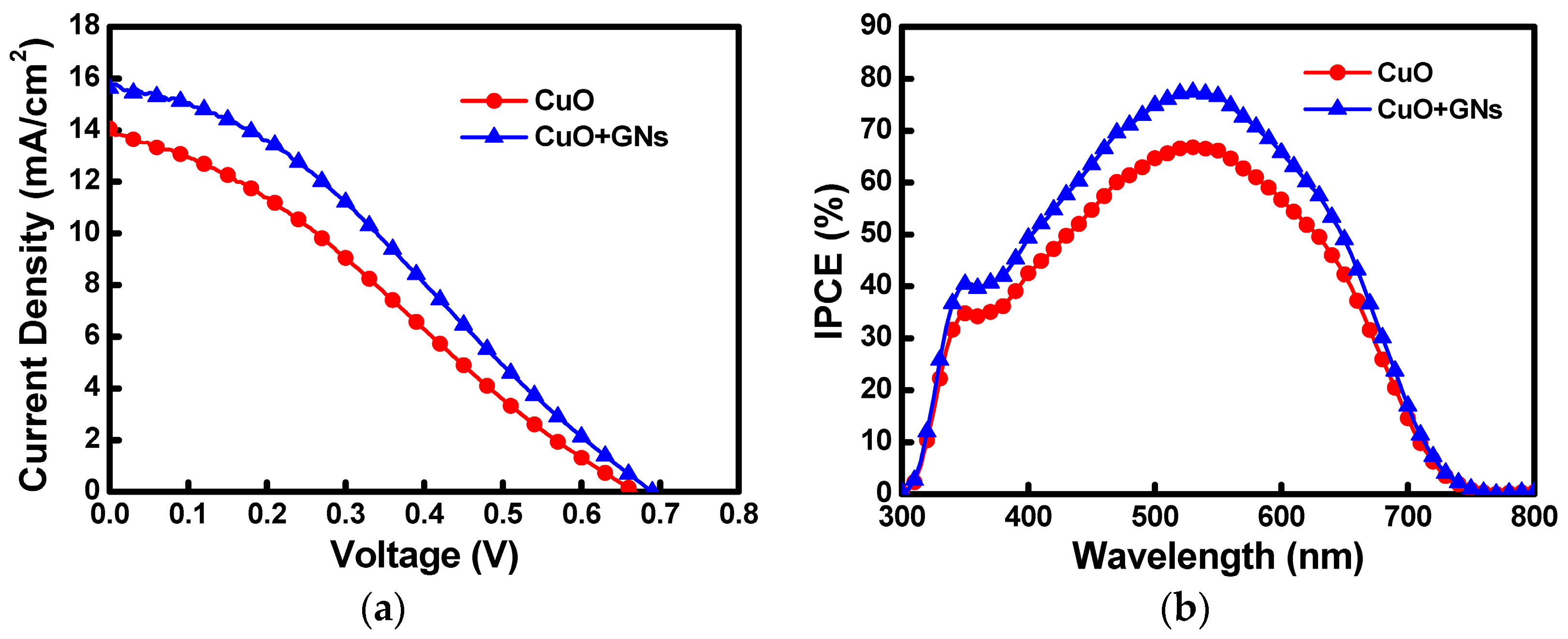
3.2. Characterization of the DSSCs

We then proceeded to fabricate DSSC devices using various CEs and investigated the effect of the different CE materials on the DSSC device properties. Figure 12a shows the JV properties of the DSSC devices fabricated using both CuO and CuO/graphene CEs. The result showed that the DSSC devices fabricated using CuO and CuO/graphene as the CEs had, respectively, Jsc values of 14.06 and 15.62 mA·cm2, Voc values of 0.67 and 0.69 V, fill factors of 0.28 and 0.31, and efficiencies of 2.73% and 3.40%. For a fair comparison, DSSCs based on Pt CEs were also fabricated and tested under similar conditions. The Jsc, Voc, and fill factor of the solar cells based on the Pt CEs were 15.12 mA·cm2, 0.69 V, and 0.61, respectively, which yielded an overall conversion efficiency of 6.36%. The measurements of each parameter are summarized in Table 1. According to the measured JV results, the DSCC fabricated using the CuO/graphene CE had a higher Jsc and power conversion efficiency than did the DSSC fabricated using CuO as the CE. However, compared with Pt, the electrical and catalytic abilities of CuO and CuO/graphene were still lower. Hence, the fill factor and power conversion efficiency of the devices fabricated with the CuO and CuO/graphene CEs were lower than those of the devices fabricated with the Pt CEs. Figure 12b shows the IPCE of the DSSC devices fabricated using the CuO and CuO/graphene CEs. The result revealed that the IPCE peak value of the DSSC device fabricated with the CuO CE was 66%, and the IPCE peak value of the DSSC device fabricated using the CuO/graphene CE was 78%. The DSSC device fabricated with the CuO/graphene CE exhibited a higher IPCE value. The IPCE result obtained is consistent with the Jsc trend obtained from the JV measurement.
The EIS (frequency range: 0.1 Hz to 1 MHz) measurements of the DSSC devices fabricated using the CuO and CuO/graphene CEs are shown in Figure 13. During the impedance measurement, the cell was under constant AM 1.5G, 100 mW·cm−2 illumination. The impedance of the cell (from 0.1 Hz to 1 MHz) was measured by applying a bias at the Voc of the cell (i.e., under no DC electric current) and by using an AC amplitude of 10 mV. In general, an impedance spectroscopy Nyquist plot contains three semicircles, which represent the interfacial impedance values of the applied CE/electrolyte (frequency range: >1 kHz), the interfacial impedance values of the applied TiO2/dye/electrolyte (frequency range: 1 Hz–1 kHz), and the impedance values of electrolytes (frequency range: 0.1–1 Hz). However, in the current study, because the TiO2/dye/electrolyte had considerably high interfacial impedance values that overlapped with the interfacial impedance values of the CEs/electrolytes and those of the electrolytes, only one semicircle was observed. To extract the quantitative impedance characteristics of the DSSCs, an equivalent-circuit model (in Figure 13) was used to analyze the internal impedance of the DSSCs. The experimental results revealed that the DSSC device fabricated using the CuO CE displayed an impedance value of approximately 600 Ω, whereas the DSSC device fabricated using the CuO/graphene CE displayed an impedance value of approximately 520 Ω. These findings reveal that the DSSC device fabricated using the CuO/graphene CE had a lower impedance value, and this is because this device featured superior catalytic abilities and material properties.

4. Conclusions

In this study, CuO and CuO/graphene pastes were coated on a FTO conductive substrate using a doctor-blade coating method. The substrate was then sintered at a high temperature to form a granular CuO nanostructure, which served as the DSSC CE. Concurrently, TiO2 working electrodes covered in dye, CuO-based CEs, and electrolytes were combined to produce DSSCs. Ethyl cellulose and terpineol were added to CuO nanoparticles and stirred to form a paste. The same methodology was adopted to produce a paste with a CuO-to-graphene weight ratio of 9:1, which was coated on conductive glass using a doctor-blade coating method. Sintering the paste under a nitrogen atmosphere and a temperature of 350 °C resulted in CuO and CuO/graphene containing a granular nanostructure. Next, an SEM, TEM, EDS, TGA, XRD, Raman spectrometer, XPS, UV-Vis spectrophotometer, and CV instrument were employed to analyze the material properties of the CuO and CuO/graphene CEs. Using the CuO and CuO/graphene CEs, a TiO2 working electrode, a dye, and an electrolyte, we fabricated DSSC devices and analyzed the device characteristics using JV, IPCE, and EIS data. The experimental results show that when CuO and CuO/graphene were used as the CEs, the device conversion efficiencies were 2.73% and 3.40%, respectively. CuO is inexpensive, abundant, nontoxic, and easy to obtain. Therefore, it is a favorable replacement for expensive Pt as a CE. Furthermore, graphene, which features high carrier mobility, may be added to enhance the electrical and catalytic abilities of CuO/graphene CEs. This is the first study to examine the use of CuO and CuO/graphene for developing Pt-free CEs in DSSCs.

Acknowledgments

The authors gratefully acknowledge the financial support from the Ministry of Science and Technology of Taiwan (MOST 106-2221-E-259-014).

Author Contributions

Chih-Hung Tsai generated ideas, designed experiments, analyzed results, supervised the entire research work, and wrote the manuscript. Po-Hsi Fei, Chia-Ming Lin, and Shiao-Long Shiu performed the experimental work and characterized the materials and devices.

Conflicts of Interest

The authors declare no conflict of interest.

References

  1. Bessho, T.; Zakeeruddin, S.M.; Yeh, C.Y.; Diau, E.W.G.; Grätzel, M. Highly efficient mesoscopic dye-sensitized solar cells based on donor–acceptor-substituted porphyrins. Angew. Chem. Int. Ed. 2010, 49, 6646–6649. [Google Scholar] [CrossRef] [PubMed]
  2. O’Regan, B.; Grätzel, M. A low-cost, high-efficiency solar cell based on dye-sensitized colloidal TiO2 films. Nature 1991, 353, 737–740. [Google Scholar] [CrossRef]
  3. Jiu, J.; Isoda, S.; Wang, F.; Adachi, M. Dye-sensitized solar cells based on a single-crystalline TiO2 nanorod film. J. Phys. Chem. B 2006, 110, 2087–2092. [Google Scholar] [CrossRef] [PubMed]
  4. Hagfeldt, A.; Grätzel, M. Molecular photovoltaics. Acc. Chem. Res. 2000, 33, 269–277. [Google Scholar] [CrossRef] [PubMed]
  5. Chiba, Y.; Islam, A.; Watanabe, Y.; Komiya, R.; Koide, N.; Han, L. Dye-sensitized solar cells with conversion efficiency of 11.1%. Jpn. J. Appl. Phys. 2006, 45, L638. [Google Scholar] [CrossRef]
  6. Chen, C.-Y.; Wang, M.; Li, J.-Y.; Pootrakulchote, N.; Alibabaei, L.; Ngoc-le, C.-H.; Decoppet, J.-D.; Tsai, J.-H.; Grätzel, C.; Wu, C.-G.; et al. Highly efficient light-harvesting ruthenium sensitizer for thin-film dye-sensitized solar cells. ACS Nano 2009, 3, 3103–3109. [Google Scholar] [CrossRef] [PubMed]
  7. Bijleveld, J.C.; Zoombelt, A.P.; Mathijssen, S.G.J.; Wienk, M.M.; Turbiez, M.; de Leeuw, D.M.; Janssen, R.A.J. Poly(diketopyrrolopyrrole−terthiophene) for ambipolar logic and photovoltaics. J. Am. Chem. Soc. 2009, 131, 16616–16617. [Google Scholar] [CrossRef] [PubMed]
  8. Yoon, J.H.; Jang, S.R.; Vittal, R.; Lee, J.; Kim, K.J. TiO2 nanorods as additive to TiO2 film for improvement in the performance of dye-sensitized solar cells. J. Photochem. Photobiol. A 2006, 180, 184–188. [Google Scholar] [CrossRef]
  9. Palomares, E.; Clifford, J.N.; Haque, S.A.; Lutz, T.; Durrant, J.R. Control of charge recombination dynamics in dye sensitized solar cells by the use of conformally deposited metal oxide blocking layers. J. Am. Chem. Soc. 2003, 125, 475–482. [Google Scholar] [CrossRef] [PubMed]
  10. Wang, P.; Klein, C.; Moser, J.E.; Humphry-Baker, R.; Cevey-Ha, N.L.; Charvet, R.; Comte, P.; Zakeeruddin, S.M.; Grätzel, M. Amphiphilic ruthenium sensitizer with 4,4’-diphosphonic acid-2,2’-bipyridine as anchoring ligand for nanocrystalline dye sensitized solar cells. J. Phys. Chem. B 2004, 108, 17553–17559. [Google Scholar] [CrossRef]
  11. Lin, L.-Y.; Tsai, C.-H.; Wong, K.-T.; Huang, T.-W.; Wu, C.-C.; Chou, S.-H.; Lin, F.; Chen, S.-H.; Tsai, A.-I. Efficient organic DSSC sensitizers bearing an electron-deficient pyrimidine as an effective π-spacer. J. Mater. Chem. 2011, 21, 5950–5958. [Google Scholar] [CrossRef]
  12. Wang, M.K.; Anghel, A.M.; Marsan, B.; Ha, N.-L.C.; Pootrakulchote, N.; Zakeeruddin, S.M.; Grätzel, M. CoS supersedes Pt as efficient electrocatalyst for triiodide reduction in dye-sensitized solar cells. J. Am. Chem. Soc. 2009, 131, 15976–15977. [Google Scholar] [CrossRef] [PubMed]
  13. Grätzel, M. Photoelectrochemical cells. Nature 2001, 414, 338–344. [Google Scholar] [CrossRef] [PubMed]
  14. Saito, Y.; Kitamura, T.; Wada, Y.; Yanagida, S. Application of poly(3,4-ethylenedioxythiophene) to counter electrode in dye-sensitized solar cells. Chem. Lett. 2002, 31, 1060–1061. [Google Scholar] [CrossRef]
  15. Saito, Y.; Kubo, W.; Kitamura, T.; Wada, Y.; Yanagida, S. I/I3 redox reaction behavior on poly(3,4-ethylenedioxythiophene) counter electrode in dye-sensitized solar cells. J. Photochem. Photobiol. A 2004, 164, 153–157. [Google Scholar] [CrossRef]
  16. Ke, C.-R.; Chang, C.-C.; Ting, J.-M. Modified conducting polymer films having high catalytic activity for use as counter electrodes in rigid and flexible dye-sensitized solar cells. J. Power Sources 2015, 284, 489–496. [Google Scholar] [CrossRef]
  17. Wei, W.; Wang, H.; Hu, Y. A review on PEDOT-based counter electrodes for dye-sensitized solar cells. Int. J. Energy Res. 2014, 38, 1099–1111. [Google Scholar] [CrossRef]
  18. Lee, K.S.; Lee, H.K.; Wang, D.H.; Park, N.-G.; Lee, J.Y.; Park, O.O.; Park, J.H. Dye-sensitized solar cells with Pt- and TCO-free counter electrodes. Chem. Commun. 2010, 46, 4505–4507. [Google Scholar] [CrossRef] [PubMed]
  19. Han, J.; Kim, H.; Kim, D.Y.; Jo, S.M.; Jang, S.Y. Water-soluble polyelectrolyte-grafted multiwalled carbon nanotube thin films for efficient counter electrode of dye-sensitized solar cells. ACS Nano 2010, 4, 3503–3509. [Google Scholar] [CrossRef] [PubMed]
  20. Choi, H.; Kim, H.; Hwang, S.; Han, Y.; Jeon, M. Graphene counter electrodes for dye-sensitized solar cells prepared by electrophoretic deposition. J. Mater. Chem. 2011, 21, 7548–7551. [Google Scholar] [CrossRef]
  21. Kitamura, K.; Shiratori, S. Layer-by-layer self-assembled mesoporous PEDOT–PSS and carbon black hybrid films for platinum free dye-sensitized-solar-cell counter electrodes. Nanotechnology 2011, 22, 195703. [Google Scholar] [CrossRef] [PubMed]
  22. Yue, G.; Wu, J.; Xiao, Y.; Lin, J.; Huang, M.; Lan, Z.; Fan, L. Functionalized graphene/poly(3,4-ethylenedioxythiophene):polystyrenesulfonate as counter electrode catalyst for dye-sensitized solar cells. Energy 2013, 54, 315–321. [Google Scholar] [CrossRef]
  23. Tsai, C.-H.; Fei, P.-H.; Chen, C.-H. Investigation of coral-like Cu2O nano/microstructures as counter electrodes for dye-sensitized solar cells. Materials 2015, 8, 5715–5729. [Google Scholar] [CrossRef] [PubMed]
  24. Berry, A.D.; Gaskill, D.K.; Holm, R.T.; Cukauskas, E.J.; Kaplan, R.; Henry, R.L. Formation of high Tc superconducting films by organometallic chemical vapor deposition. Appl. Phys. Lett. 1988, 52, 1743. [Google Scholar] [CrossRef]
  25. Abaker, M.; Dar, G.N.; Umar, A.; Zaidi, S.A.; Ibrahim, A.A.; Baskoutas, S.; Al-Hajry, A. CuO nanocubes based highly-sensitive 4-nitrophenol chemical sensor. Sci. Adv. Mater. 2012, 4, 893–900. [Google Scholar] [CrossRef]
  26. Borkow, G.; Gabbay, J.; Lyakhovitsky, A.; Huszar, M. Improvement of facial skin characteristics using copper oxide containing pillowcases: A double-blind, placebo-controlled, parallel, randomized study. Int. J. Cosmet. Sci. 2009, 31, 437–443. [Google Scholar] [CrossRef] [PubMed]
  27. Xu, J.; Ji, W.; Shen, Z.; Tang, S.; Ye, X.; Jia, D.; Xin, X. Preparation and characterization of CuO nanocrystals. J. Solid State Chem. 1999, 147, 516–519. [Google Scholar] [CrossRef]
  28. Carnes, C.L.; Stipp, J.; Klabunde, K.J. Synthesis, characterization, and adsorption studies of nanocrystalline copper oxide and nickel oxide. Langmuir 2002, 18, 1352–1359. [Google Scholar] [CrossRef]
  29. Habibi, M.H.; Karimi, B.; Zendehdel, M.; Habibi, M.; Habibi, M. Fabrication, characterization of two nano-composite CuO–ZnO working electrodes for dye-sensitized solar cell. Spectrochim. Acta Mol. Biomol. Spectrosc. 2013, 116, 374–380. [Google Scholar] [CrossRef] [PubMed]
  30. Novoselov, K.S.; Geim, A.K.; Morozov, S.V.; Jiang, D.; Zhang, Y.; Dubonos, S.V.; Grigorieva, I.V.; Firsov, A.A. Electric field effect in atomically thin carbon films. Science 2004, 306, 666–669. [Google Scholar] [CrossRef] [PubMed]
  31. Cao, Y.; Liu, S.; Shen, Q.; Yan, K.; Li, P.; Xu, J.; Yu, D.; Steigerwald, M.L.; Nuckolls, C.; Liu, Z.; et al. High-performance photoresponsive organic nanotransistors with single-layer graphenes as two-dimensional electrodes. Adv. Func. Mater. 2009, 19, 2743–2748. [Google Scholar] [CrossRef]
  32. Kavan, L.; Yum, J.H.; Grätzel, M. Optically transparent cathode for dye-sensitized solar cells based on graphene nanoplatelets. ACS Nano 2011, 5, 165–172. [Google Scholar] [CrossRef] [PubMed]
  33. Yu, Y.-H.; Chi, W.-F.; Huang, W.-C.; Wang, W.-S.; Shih, C.-J.; Tsai, C.-H. High-efficiency counter electrodes using graphene hybrid with a macrocyclic nickel complex for dye-sensitized solar cells. Org. Electron. 2016, 31, 207–216. [Google Scholar] [CrossRef]
  34. Tsai, C.-H.; Huang, W.-C.; Wang, W.-S.; Shih, C.-J.; Chi, W.-F.; Hu, Y.-C.; Yu, Y.-H. Reduced graphene oxide/macrocyclic iron complex hybrid materials as counter electrodes for dye-sensitized solar cells. J. Colloid Interface Sci. 2017, 495, 111–121. [Google Scholar] [CrossRef] [PubMed]
  35. Zhang, D.; Li, X.; Li, H.; Chen, S.; Sun, Z.; Yin, X.; Huang, S. Graphene-based counter electrode for dye-sensitized solar cells. Carbon 2011, 49, 5382–5388. [Google Scholar] [CrossRef]
  36. Roy-Mayhew, J.D.; Bozym, D.J.; Punckt, C.; Aksay, I.A. Functionalized graphene as a catalytic counter electrode in dye-sensitized solar cells. ACS Nano 2010, 4, 6203–6211. [Google Scholar] [CrossRef] [PubMed]
Figure 1. Preparation processes of CuO and CuO/graphene pastes.
Coatings 08 00021 g001
Figure 2. The schematic device structure of a DSSC using the CuO or CuO/graphene CEs.
Coatings 08 00021 g002
Figure 3. Top-view SEM images of (a) CuO and (b) CuO/graphene CEs. Cross-sectional SEM images of (c) CuO and (d) CuO/graphene CEs.
Coatings 08 00021 g003
Figure 4. SEM images of CuO CEs fabricated with (a) 20 wt % and (b) 30 wt % CuO nanoparticles in CuO pastes. SEM images of CuO/graphene CEs fabricated with (c) CuO:GNs (9:1) and (d) CuO:GNs (8:2) weight ratios in CuO/graphene pastes.
Coatings 08 00021 g004
Figure 5. The TEM image of CuO/graphene counter electrode.
Coatings 08 00021 g005
Figure 6. EDS analysis results of (a) CuO and (b) CuO/graphene CEs.
Coatings 08 00021 g006
Figure 7. TGA analysis results of CuO and CuO/graphene CEs.
Coatings 08 00021 g007
Figure 8. Raman spectra of CuO and CuO/graphene CEs.
Coatings 08 00021 g008
Figure 9. XRD spectra of CuO and CuO/graphene CEs.
Coatings 08 00021 g009
Figure 10. (a) XPS analysis results and (b) transmittance spectra of CuO and CuO/graphene CEs.
Coatings 08 00021 g010
Figure 11. Cyclic voltammograms of CuO and CuO/graphene CEs.
Coatings 08 00021 g011
Figure 12. (a) JV curves and (b) IPCE curves of DSSCs using CuO and CuO/graphene CEs.
Coatings 08 00021 g012
Figure 13. EIS Nyquist plots of DSSCs using CuO and CuO/graphene CEs.
Coatings 08 00021 g013
Table 1. Characteristics of DSSCs fabricated using various counter electrodes.
Counter ElectrodeJsc (mA/cm2)Voc (V)Fill FactorEfficiency (%)
CuO14.060.670.282.73
CuO + GNs15.620.690.313.40
Pt15.120.690.616.36

