1. Introduction
Thermoelectric materials, which can directly convert thermal energy to electric energy, have attracted a significant amount of attention due to their promising applications in solid state cooling and power generation from waste heat [
1,
2,
3,
4]. The efficiency of thermoelectric generators is determined by the thermoelectric performance of such materials; it is determined by the dimensionless figure of merit,
ZT, which is defined as
ZT = S2σ
T/κ, where
S corresponds to the Seebeck coefficient, σ refers to the electrical conductivity,
T represents the absolute temperature, and κ is the thermal conductivity [
5]. High-performance thermoelectric materials require high Seebeck coefficient and electrical conductivity as well as low thermal conductivity [
6]. Thin films have been demonstrated as low-dimensional systems that can enhance the thermoelectric performance of materials due to their dense interfaces and grain boundaries, which can effectively scatter phonons [
7,
8,
9,
10]. For example, a high room temperature figure of merit of
ZT = 2.4 has been reported for p-type Bi
2Te
3/Sb
2Te
3 superlattices [
11], and such a result is attributed to quantum confinement effects.
CoSb
3 is one of the numerous promising thermoelectric materials in the intermediate temperature range [
12,
13,
14,
15]. This material possesses a special skutterudite structure with two lattice voids, which can be filled with rare elements that can scatter a wide range of phonons and enhance thermoelectric properties. In recent years, several studies on the synthesis of CoSb
3-based thin films have been investigated [
16,
17,
18]; for instance, Kumar et al. [
17] obtained a power factor (PF) of 0.97 mW·m
−1·K
−2 for In- and Yb-co-doped CoSb
3 films deposited by pulsed laser deposition. However, the thermoelectric properties of CoSb
3 thin films remain lower than those of bulk materials due to the difficulty in controlling element composition from raw materials to thin films during preparation.
Radio frequency (RF) magnetron sputtering is an attractive technique for preparing thin films for industrial development [
19]. We observed that CoSb
3 thin films can be obtained by RF magnetron sputtering after annealing [
20,
21,
22], but they contain an excess amount of Sb and display poor thermoelectric properties; unlike in bulk materials, excess Sb exerts a negative influence on thin films [
23,
24]. This difference may be attributed to the amorphous state of excess Sb in thin films [
20,
23,
24]. Conversely, thin films show an unnecessary additional CoSb
2 phase that positively affects their thermoelectric properties. Therefore, in the current work, CoSb
3 thin films were deposited by RF magnetron sputtering, and their composition was regulated along with substrate temperature during thin film growth. The microstructure of thin films was investigated and compared with that of thin films under annealing [
21,
22]. The influence of microstructure on thermoelectric properties was also interpreted to improve the thermoelectric performance of thin films via microstructure optimization.
2. Materials and Methods
CoSb3 alloy targets with Co:Sb atomic ratios of 1:3 and 1:3.5 were set in a JGP-450B double chamber magnetron sputtering ultrahigh vacuum system (Shenyang Science Instrument of Chinese Academy of Sciences, Shenyang, China). BK7 glass measuring 20 mm × 20 mm × 2 mm was used as a substrate and erased cleanly by air-laid paper after ultrasonic cleaning for 20 min in acetone, alcohol, and deionized water. A 5-min pre-sputtering process was carried out to remove contaminants on the target surface. The chamber was pumped down to 6.0 × 10⁻⁴ Pa, and working pressure measured 0.4 Pa with 40.0 sccm Ar. Before deposition, the substrate was heated to a setting temperature and kept stable. The temperature was set from 225 to 325 °C at 25 °C intervals. Then, thin films were grown at the substrate by RF magnetron sputtering with 50 W power. The thin films prepared with 1:3 target were labeled as T-series (T1–T5), and samples prepared with 1:3.5 target were labeled as S-series (S1–S5).
Structural phase formation in films was investigated by X-ray diffraction (XRD; D/max 2500, Rigaku Corporation, Tokyo, Japan) with the prescriptive θ–2θ mode and a determined incident angle of 10–80° using Cu Kα radiation (λ = 0.15406 nm). Surface morphology was analyzed by scanning electron microscopy (SEM) (Zeiss supra 55, Carl Zeiss, Oberkochen, Germany), whereas component analysis was performed via energy dispersive spectroscopy (EDS, Quantax, Bruker, Karlsruhe, Germany) with the error of <10%. Electrical conductivity σ and Seebeck coefficient S were measured by the simultaneous determination of the Seebeck coefficient and electrical conductivity system (Netzsch SBA458, Netzsch, Shanghai, China) in the interval of 323–573 K.
3. Results
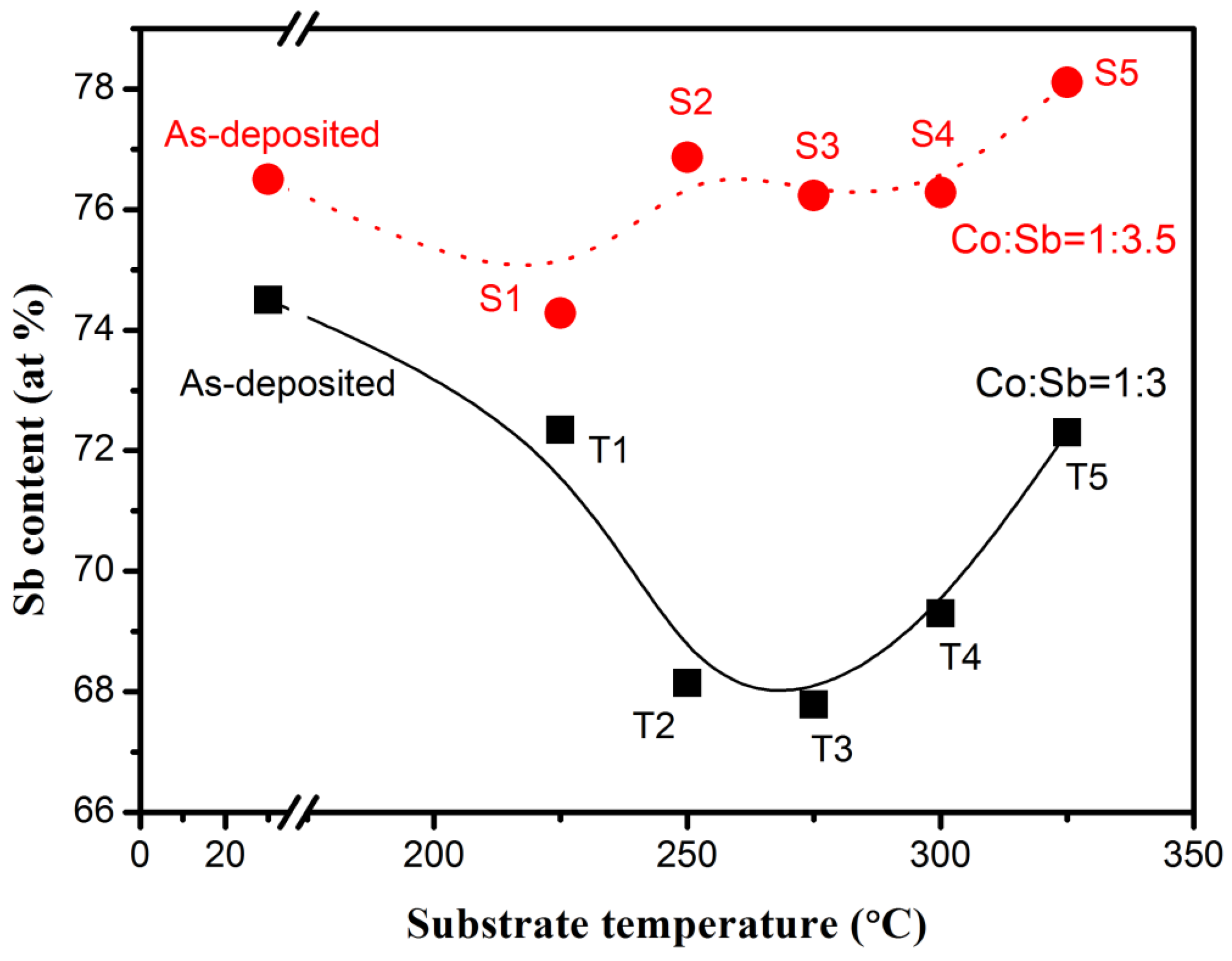
Sb content was determined by EDS, along with the as-deposited thin films.
Figure 1 presents the results. The figure shows that the samples (prepared with Co:Sb = 1:3.5 target) approached the 75% stoichiometric ratio, and that the Sb content decreased slightly with increasing deposition temperature due to the evaporation of Sb. Nevertheless, most of the thin films contained abundant Sb. The as-deposited thin films (prepared with Co:Sb = 1:3 target) showed a minimal lack of Sb, but Sb content decreased remarkably when the deposition temperature increased. The Sb content increased at high deposition temperatures in both samples prepared with different targets. This characteristic is presumably related to the enhancement of the Co evaporation effect at high temperatures.
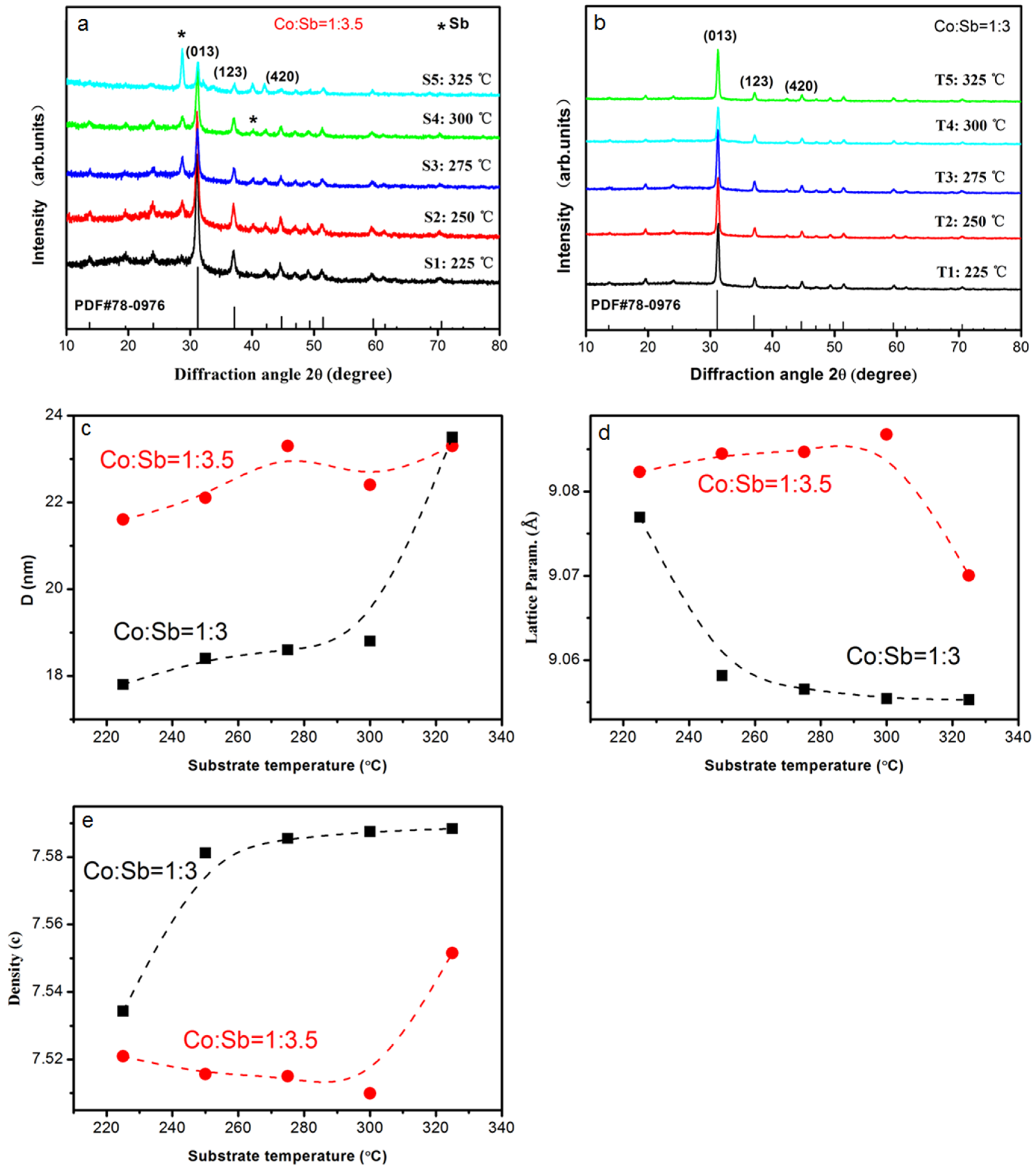
Figure 2a,b show the XRD patterns of thin films prepared with different targets, including the characteristic pattern of CoSb
3 (PDF#780976). As shown in
Figure 2a, the strongest diffraction peak of sample S1 was located at ~31°, which is related to the (310) plane of the CoSb
3 phase. Most peaks also correspond to the characteristic diffraction peak, indicating that the sample featured a primary CoSb
3 phase. A few peaks of impurity can be observed in the pattern, and these peaks are related to the hexagonal Sb structure as the secondary phase. With increasing the deposition temperature, a similar result can be obtained, with CoSb
3 as the primary phase and Sb as the secondary phase, as indicated in XRD patterns of S2–S5. However, the intensity of the impurity peaks increased with increasing temperature, and the intensity of the peak located at 29° became the strongest when deposition temperature reached 325 °C. This result indicates that the Sb phase transformed into the primary phase of sample S5.
Figure 2b shows that all thin films prepared with Co:Sb = 1:3 target yielded three major diffraction peaks, which were indexed as reflection planes from (013), (123), and (211) of the CoSb
3 phase. No impurity peaks could be observed from the patterns of these thin films, thereby indicating that all samples comprised a single CoSb
3 phase and were well-crystallized. Crystallite size D was calculated from XRD data using the Debye–Sherrer Equation: D = κ·λ/β
2θ·cosθ, where λ represents the wavelength, β
2θ refers to the full width at half maximum, and θ is the angle [
25].
Figure 2c shows the calculation results of the peak related to the (013) plane. Results showed that the crystallite size of all thin films increased with increasing deposition temperature. Such an increase suggests that the thermal effects can efficiently promote thin film growth. The grain size of samples prepared with the 1:3.5 target was larger than that of thin films prepared with the 1:3 target. Lattice parameter and crystal density were calculated by using the full-profile Rietveld refinement method and are shown in
Figure 2d,e, respectively. Samples with excess Sb featured a large lattice parameter, possibly due to excess Sb filling the CoSb
3 cubic void during the growth process. This condition caused the expansion of the unit cell and large grain size. In general, thin films with a large grain size showed good electrical conductivity due to lower interface scattering. However, the lattice density of T1–T5 was much higher than that of S1–S5, and it followed an increasing trend when the deposition temperature increased. This result indicates that thin films possess a more compact structure and fewer defects than that of S-series samples. These properties benefit electron transport and should lead to improved thermoelectric properties.
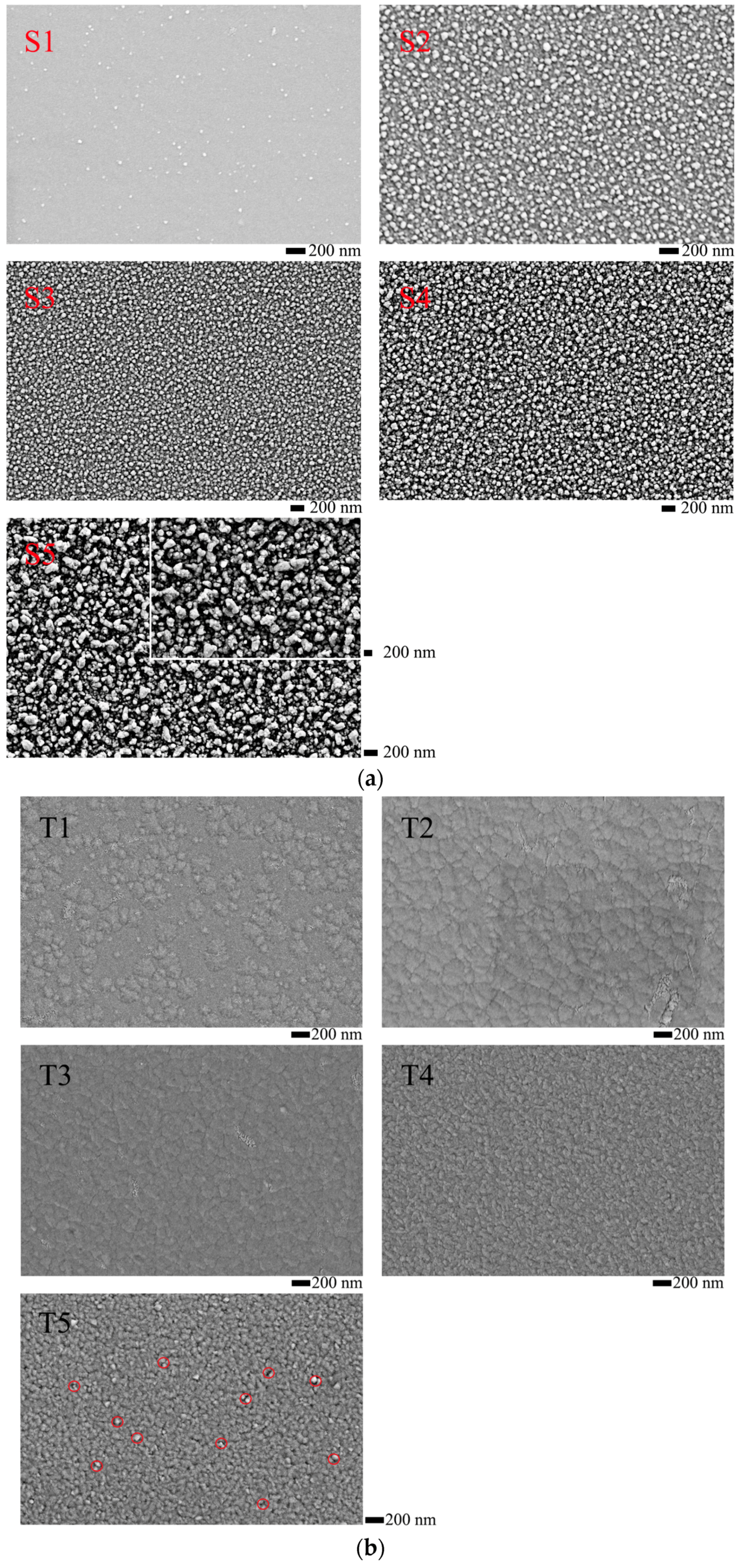
Figure 3a shows surface morphology of thin films S1–S5. The grain size increased with rising deposition temperature, and this condition was consistent with results of the XRD analysis. However, grains were not normalized and thus caused the formation a rough and loose structure. As shown in the illustration of S5 in
Figure 3a, the grains size of the thin films increased with increasing temperature. However, the grains revealed nonnormalized size and shape, especially in sample S5, which presented numerous large hexagonal-like clusters; such clusters indicate the clustering of excess Sb atoms. The surface morphology of CoSb
3 thin films T1–T5 was also measured, and results are shown in
Figure 3b. The results reveal that T1–T4 samples exhibited a smooth surface across all regions. The film surface became increasingly dense, and grains were normalized with increasing temperature. These findings signify that dense thin films with minimal crystal imperfection can be obtained. Although T5 features a dense structure, a number of impure large grains and a porous surface can be observed (marked as red region). These characteristics indicate that thin films exhibited a number of defects that would adversely affect electron transport when the deposition temperature was extremely high.
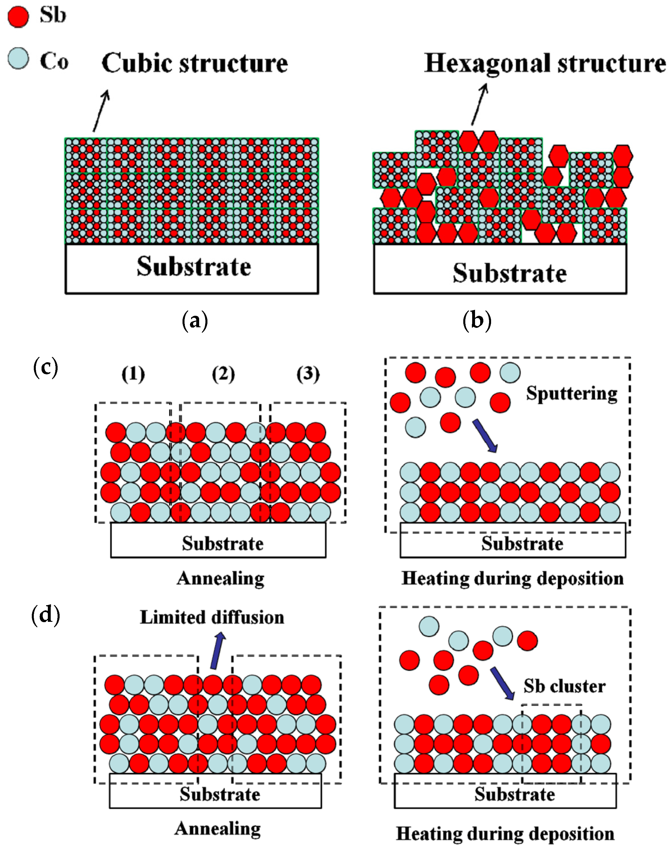
Based on the thin film growth model [
26,
27], the mechanism considered in the present study is illustrated in
Figure 4a,b. The substrate used in this work is an amorphous BK7 glass with a flat surface. In general, thin films followed the growth pattern shown in the Frank-van der Merwe model (layer growth). As presented in
Figure 4a, grains crystallized preferentially based on substrate morphology at an early stage. Then, layer fabrication followed that of the preformed layer during the growth process. Thus, the thin films with a single CoSb
3 phase exhibited less phase defects, and the cubic structure led to a dense and smooth surface, as shown in
Figure 3b. Similarly, the thin films formed a CoSb
3 structure, along with some hexagonal Sb grains, as shown in the same process shown in
Figure 4b. This growth mode caused the formation of progressive interface voids and a loose structure (
Figure 3a). A particularly different growth phenomenon was obtained by comparison with the results of annealed samples in our early works [
21,
22]. The samples deficient in Sb showed a secondary CoSb
2 phase, whereas those with excess Sb phase formed only when the temperature was higher than 600 K. Thus, the mechanism behind such differences was also investigated. As presented in
Figure 4c, the thin films exhibited a stable composition distribution before annealing, and the elements failed to diffuse extensively. When the thin films presented Sb deficiency, regions such as (1) and (3), which are distributed with sufficient Sb, grew CoSb
3 crystals, whereas some regions such as (2) lacked Sb and crystallized with a CoSb
2 structure. Grain crystallization occurred during sputtering when the substrate was heated, and Sb was continuously supplied to guarantee the fabrication of a single structure. Similarly, crystals grew with a CoSb
3 structure when the thin films contained superfluous Sb (
Figure 4d). However, Sb crystals did not easily form at low temperatures by limited diffusion because of the existence of nucleating CoSb
3 acting as the barrier layer. Conversely, hexagonal Sb grains could easily be clustered and crystallized when all grains grew in the same process at a low temperature.
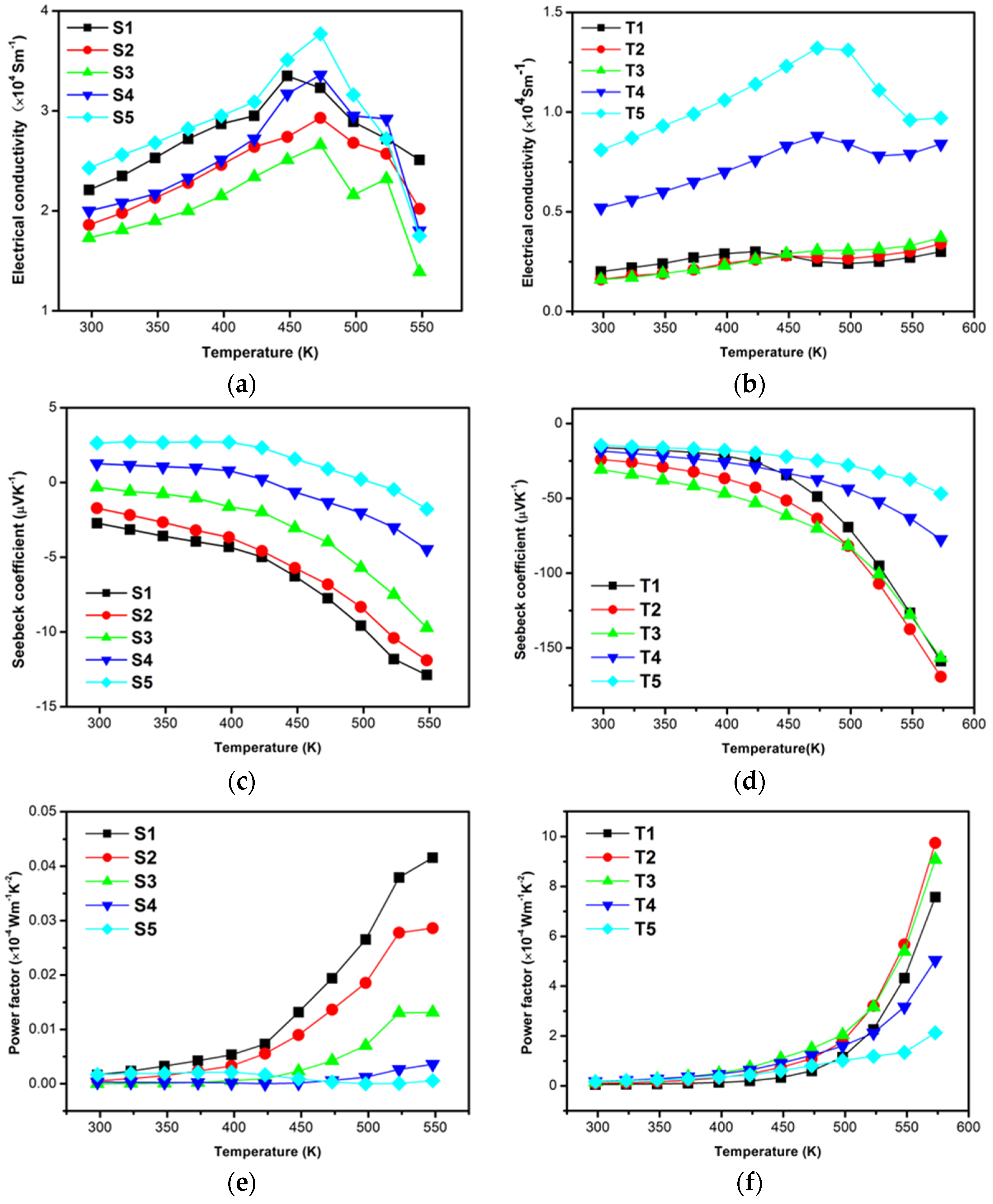
Figure 5a,b show electrical conductivity, σ, as the function of temperature. In
Figure 5a, the electrical conductivities of samples S1–S5 shared similar values around 2.0 × 10
4 S·m
−1 at 300 K, and increased with increasing temperature. Comparatively, S5 yielded a slightly higher electrical conductivity at 300 K due to its large grain size; its maximum value measured 3.7 × 10
4 S·m
−1 at 473 K. However, the electrical conductivities of samples decreased dramatically at 450 K and dropped to extremely low values when the temperature reached 550 K. This result can be attributed to the loose structure, which can easily introduce oxidation defects and result in the decline of σ. As shown in
Figure 5b, the electrical conductivity, σ, increased with increasing deposition temperature. This result was consistent with the enhancement of grain size. T5 presented the highest electrical conductivity among the samples, reaching a maximum value of 1.3 × 10
4 S·m
−1 at 473 K, and then decreased when the temperature continually increased. Although σ values of the T-series samples were lower than those of the S-series samples, they were steadier in terms of their thermal conductivities because of their dense structure, which prevents defects at high temperatures.
Figure 5c,d illustrate the influence of substrate temperature on the Seebeck coefficients,
S, of the thin films. As shown in
Figure 5c, the Seebeck coefficients of S1, S2, and S3 were negative at room temperature, whereas those of S4 and S5 were positive. This result is attributed to impure Sb crystallization, which constantly exhibited a p-type conduction according to the combined results of microstructure measurement.
S of S1 to S3 increased with increasing temperature, and S1 yielded a maximum value of −12.87 μV·K
−1 at 550 K. However, the value was extremely lower than those of CoSb
3 bulk materials. Interestingly,
S values of S4 and S5 decreased with increasing temperature and transformed into n-types when the measurement temperature reached a certain high point, possibly as a result of the anabatic oxidation effect. As presented in
Figure 5d, the thin films presented negative Seebeck coefficients, and the values were close to each other at low temperatures. Absolute values of all samples increased when temperature increased. In particular, the Seebeck coefficients of T1, T2, and T3 showed a sharp increase in their absolute values, which reached −170 μV·K
−1 at 573 K, possibly due to their structure being denser and more crystallized than that of samples fabricated at high temperatures.
PF, one of the important thermoelectric parameters, determines thermoelectric energy conversion and is defined as S
2σ. The temperature dependence of PF is shown in
Figure 5e,f. As shown in
Figure 5e, PF of S1–S5 showed an increasing trend, but the values were extremely low and decreased with deposition temperature at high temperatures. Different from that of the S-series samples, PF of the T-series samples was much higher and sharply increased when temperature >450 K due to the high Seebeck coefficient in
Figure 5f. T2 and T3 respectively obtained maximum PF values of 9.8 × 10
−4 and 9.1 × 10
−4 W·m
−1·K
−2, which were almost 20 times higher than those of the S-series samples.


