Chemical Vapor Deposition of Bi-Te-Ni-Fe on Magnesium Oxide Substrate and Its Seebeck Effect


Abstract
:1. Introduction
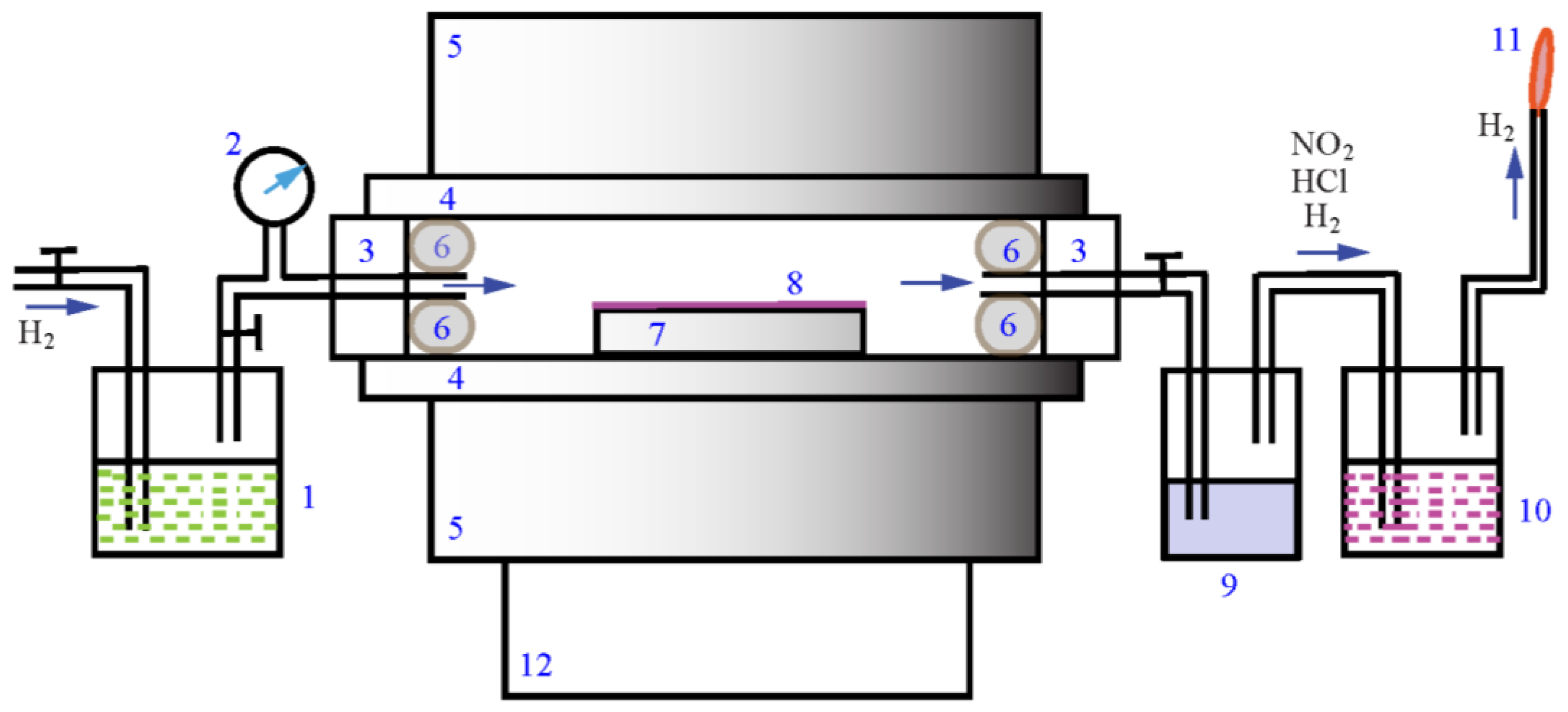
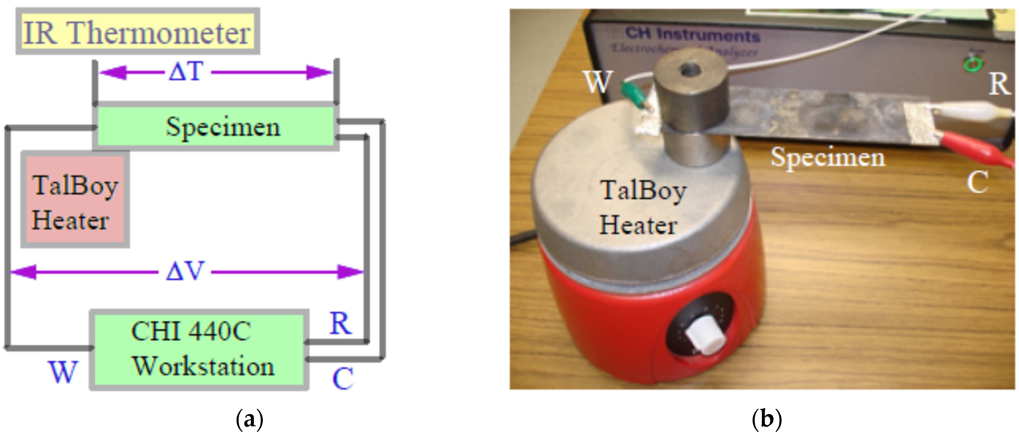
2. Materials and Experimental Methods
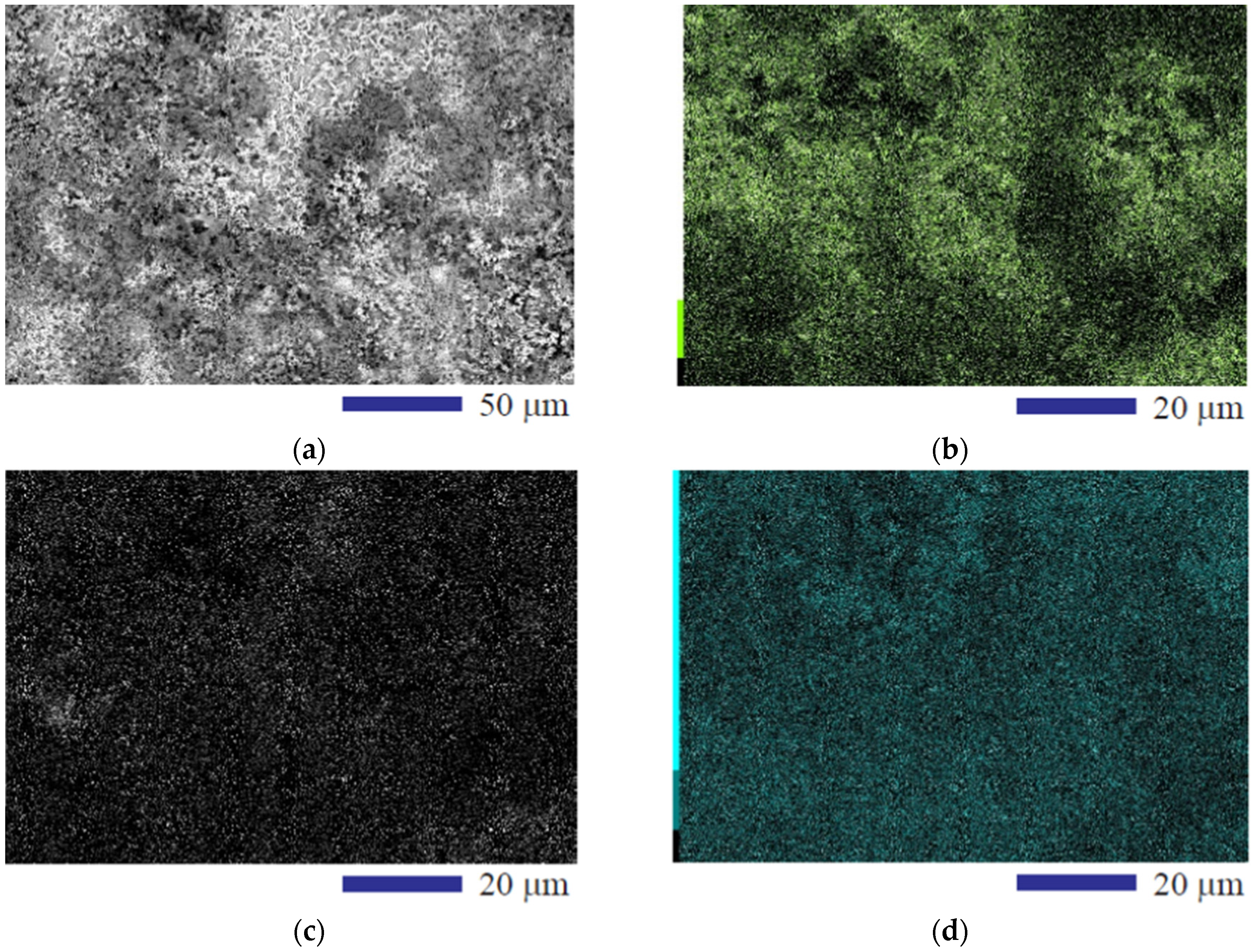
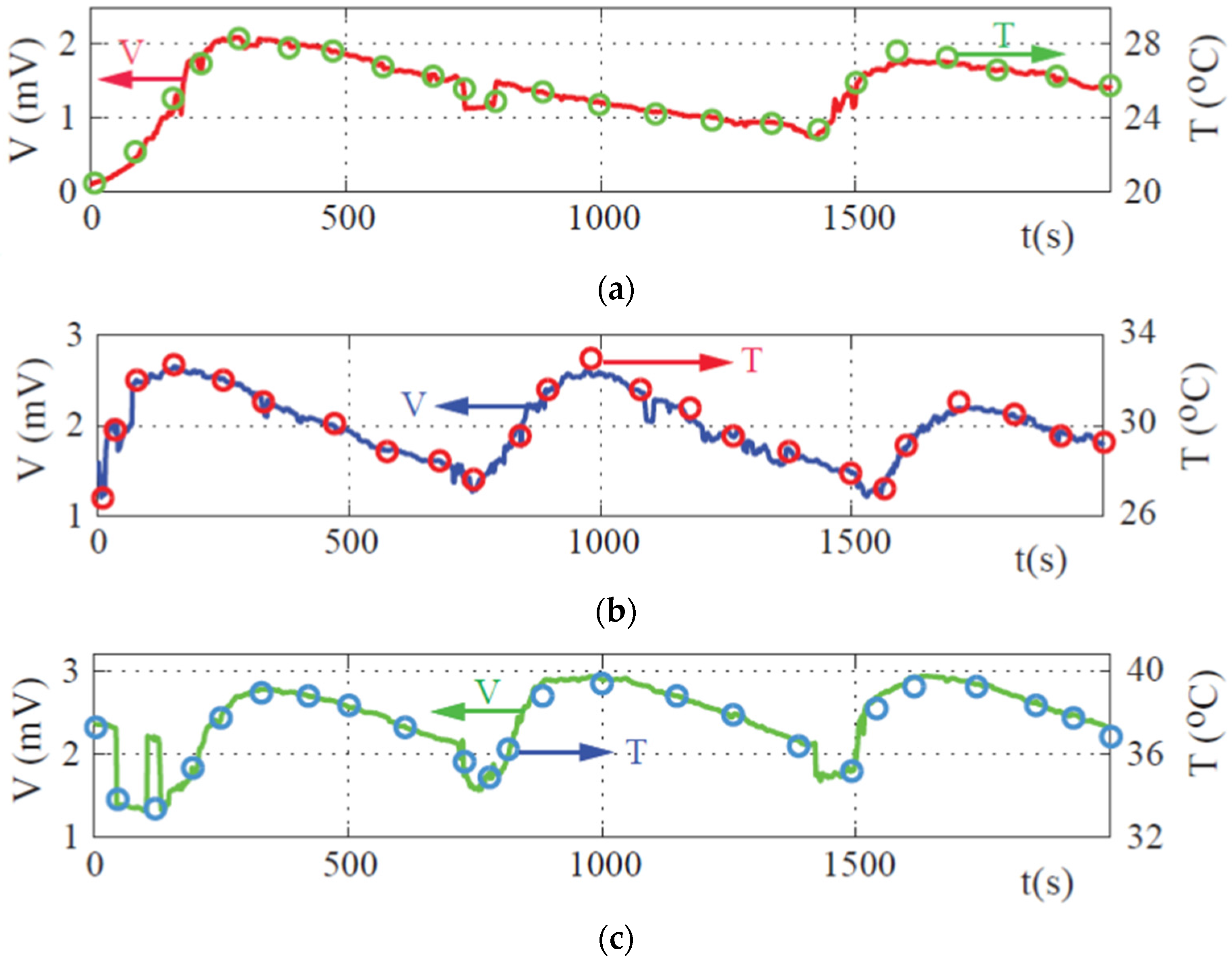
3. Results and Discussion
4. Conclusions
Acknowledgments
Author Contributions
Conflicts of Interest
References
- Huang, G.; Jian, J.; Lei, R.; Cao, B. Single-crystalline Bi2Se3 nanowires grown by catalyst-free ambient pressure chemical vapor deposition. Mater. Lett. 2016, 179, 198–201. [Google Scholar] [CrossRef]
- Tynell, T.; Aizawa, T.; Ohkubo, I.; Nakamura, K.; Mori, T. Deposition of thermoelectric strontium hexaboride thin films by a low pressure CVD method. J. Cryst. Growth 2016, 449, 10–14. [Google Scholar] [CrossRef]
- Chen, P.; Wang, J.; Lu, Y.; Zhang, S.; Liu, X.; Hou, W.; Wang, Z.; Wang, L. The fabrication of ReS2 flowers at controlled locations by chemical vapor deposition. Phys. E Low-Dimens. Syst. Nanostruct. 2017, 89, 115–118. [Google Scholar] [CrossRef]
- Haase, A.; Peters, A.; Rosiwal, S. Growth and thermoelectric properties of nitrogen-doped diamond/graphite. Diam. Relat. Mater. 2016, 63, 222–226. [Google Scholar] [CrossRef]
- Hewitt, C.A.; Carroll, D.L. The effects of acid treatment on the thermoelectric power of multiwalled carbon nanotubes synthesized by chemical vapor deposition. Chem. Phys. Lett. 2013, 580, 67–72. [Google Scholar] [CrossRef]
- Kunadian, I.; Lipka, S.M.; Swartz, C.R.; Qian, D.; Andrews, R. Determination of carrier densities of boron- and nitrogen-doped multiwalled carbon nanotubes using Mott-Schottky plots. J. Electrochem. Soc. 2009, 156, K110–K115. [Google Scholar] [CrossRef]
- Cademartiri, L.; Ozin, G.A. Ultrathin nanowires—A materials chemistry perspective. Adv. Mater. 2009, 21, 1013–1020. [Google Scholar] [CrossRef]
- Balducci, A.; Marinelli, M.; Morgada, M.E.; Pucella, G.; Rodriguez, G.; Scoccia, M.; Verona-Rinati, G. CVD-diamond-based thermocouple for high sensitive temperature measurements. Microsyst. Technol. 2006, 12, 365–368. [Google Scholar] [CrossRef]
- Balducci, A.; D’Amico, A.; Di Natale, C.; Marinelli, M.; Milani, E.; Morgada, M.E.; Pucella, G.; Rodriguez, G.; Tucciarone, A.; Verona-Rinati, G. High performance CVD-diamond-based thermocouple for gas sensing. Sens. Actuators B 2005, 111, 102–105. [Google Scholar] [CrossRef]
- Eaton, S.C.; Anderson, A.B.; Angus, J.C.; Evstefeeva, Y.E.; Pleskov, Y.V. Diamond growth in the presence of boron and sulfur. Diam. Relat. Mater. 2003, 12, 1627–1632. [Google Scholar] [CrossRef]
- Horiuchi, R.; Okano, K.; Rupesinghe, N.; Chhowalla, M.; Amaratunga, G.A.J. Seebeck measurements of N-doped diamond thin film. Phys. Stat. Sol. A 2002, 193, 457–461. [Google Scholar] [CrossRef]
- Souw, E.K.; Meilunas, R.J.; Szeles, C.; Ravindra, N.M.; Tong, F.M. Photoconductivity of CVD diamond under bandgap and subbandgap irradiations. Diam. Relat. Mater. 1997, 6, 1157–1171. [Google Scholar] [CrossRef]
- Saitoh, H.; Ishikawa, M.; Urao, R. Substrate temperature measured by a film-on-plate thermocouple during diamond growth using the combustion flame technique. Diam. Relat. Mater. 1995, 4, 1056–1060. [Google Scholar] [CrossRef]
- DaVila, D.; Tarancon, A.; Calaza, C.; Salleras, M.; Fernandez-Regulez, M.; San Paulo, A.; Fonseca, L. Improved thermal behavior of multiple linked array of silicon nanowires integrated into planar thermoelectric microgenerators. J. Electron. Mater. 2013, 42, 1918–1925. [Google Scholar] [CrossRef]
- Wu, Y.; Fan, R.; Yang, P. Block-by-block growth of single-crystalline Si/SiGe superlattice nanowires. Nano Lett. 2002, 2, 83–86. [Google Scholar] [CrossRef]
- Kim, J.G.; Choi, Y.Y.; Choi, D.J.; Choi, S.M. Study on the thermoelectric properties of CVD SiC deposited with inert gases. J. Electron. Mater. 2011, 40, 840–844. [Google Scholar] [CrossRef]
- Kim, J.G.; Choi, Y.Y.; Choi, D.J.; Kim, J.I.; Kim, B.S.; Choi, S.M. A study on the thermoelectric property of chemical vapor deposited SiC films with temperature and diluent gases variations. J. Ceram. Soc. Jan. 2009, 117, 574–577. [Google Scholar] [CrossRef]
- Tajima, K.; Shin, W.; Murayama, N.; Itoh, T.; Izu, N.; Matsubara, I. Preparation of phosphorus-doped Si0.8Ge0.2 thermoelectric thin films using RF sputtering with induction coil. J. Ceram. Soc. Jan. 2005, 113, 558–561. [Google Scholar] [CrossRef]
- Yoshinaga, M.; Iida, T.; Noda, M.; Endo, T.; Takanashi, Y. Bulk crystal growth of Mg2Si by the vertical Bridgman method. Thin Solid Films 2004, 461, 86–89. [Google Scholar] [CrossRef]
- Mukaida, M.; Hiyama, I.; Tsunoda, T.; Imai, Y. Preparation of β-FeSi2 films by chemical vapor deposition. Thin Solid Films 2001, 381, 214–218. [Google Scholar] [CrossRef]
- Akiyama, K.; Ohya, S.; Funakubo, H. Preparation of β-FeSi2 thin film by metal organic chemical vapor deposition using iron-carbonyl and mono-silane. Thin Solid Films 2004, 461, 40–43. [Google Scholar] [CrossRef]
- Kumashiro, Y.; Nakamura, K.; Enomoto, T.; Tanaka, M. Preparation and thermoelectric properties of BP films on SOI and sapphire substrates. J. Mater. Sci. Mater. Electron. 2011, 22, 966–973. [Google Scholar] [CrossRef]
- Komatsu, S.; Sato, Y.; Hirano, D.; Nakamura, T.; Koga, K.; Yamamoto, A.; Nagata, T.; Chikyo, T.; Watanabe, T.; Takizawa, T.; et al. P-type sp3-bonded BN/n-type Si heterodiode solar cell fabricated by laser-plasma synchronous CVD method. J. Phys. D Appl. Phys. 2009, 42, 225107. [Google Scholar] [CrossRef]
- Wang, Z.; Shimizu, Y.; Sasaki, T.; Kirihara, K.; Kawaguchi, K.; Kimura, K.; Koshizaki, N. Fabrication of crystallized boron films by laser ablation. J. Solid State Chem. 2004, 177, 1639–1645. [Google Scholar] [CrossRef]
- Kumashiro, Y.; Enomoto, T.; Sato, K.; Abe, Y.; Hirata, K.; Yokoyama, T. Thermoelectric properties of photo- and thermal CVD boron and boron phosphide films. J. Solid State Chem. 2004, 177, 529–532. [Google Scholar] [CrossRef]
- Kumashiro, K.; Hirata, K.; Sato, K.; Yokoyama, T.; Aisu, T.; Ikeda, T.; Minaguchi, M. Thermoelectric properties of boron and boron phosphide films. J. Solid State Chem. 2000, 154, 26–32. [Google Scholar] [CrossRef]
- Kumashiro, Y.; Yokoyama, T.; Sato, A.; Ando, Y. Thermoelectric properties of boron and boron phosphide CVD wafers. J. Solid State Chem. 1997, 133, 314–321. [Google Scholar] [CrossRef]
- Suematsu, H.; Kitajima, K.; Ruiz, I.; Kobayashi, K.; Takeda, M.; Shimbo, D.; Suzuki, T.; Jiang, W.; Yatsui, K. Thermoelectric properties of crystallized boron carbide thin films prepared by ion-beam evaporation. Thin Solid Films 2002, 407, 132–135. [Google Scholar] [CrossRef]
- Sezer, A.O.; Brand, J.I. Chemical vapor deposition of boron carbide. Mater. Sci. Eng. B 2001, 79, 191–202. [Google Scholar] [CrossRef]
- Kumasiro, Y.; Yokoyama, T.; Sakamoto, T.; Fujita, T. Preparation and electrical properties of boron and boron phosphide films obtained by gas source molecular beam deposition. J. Solid State Chem. 1997, 133, 269–272. [Google Scholar] [CrossRef]
- Ngamou, P.H.T.; Bahlawane, N. Chemical vapor deposition and electric characterization of perovskite oxides LaMO3 (M = Co, Fe, Cr and Mn) thin films. J. Solid State Chem. 2009, 182, 849–854. [Google Scholar] [CrossRef]
- Cho, H.S.; Kamins, T.I. In situ control of Au catalyzed chemical vapor deposited (CVD) Ge nanocone morphology by growth temperature variation. J. Cryst. Growth 2010, 312, 2494–2497. [Google Scholar] [CrossRef]
- Grigorian, L.; Fang, S.; Sumanasekera, G.; Rao, A.M.; Schrader, L.; Eklund, P.C. Physical properties of CVD-grown Se-carbon films. Synth. Met. 1997, 87, 211–217. [Google Scholar] [CrossRef]
- Giani, A.; Boulouz, A.; Pascal-Delannoy, F.; Foucaran, A.; Boyer, A. MOCVD growth of Bi2Te3 layers using diethyltellurium as a precursor. Thin Solid Films 1998, 315, 99–103. [Google Scholar] [CrossRef]
- Giani, A.; Boulouz, A.; Pascal-Delannoy, F.; Foucaran, A.; Boyer, A. Growth of Bi2Te3 and Sb2Te3 thin films by MOCVD. Mater. Sci. Eng. B 1999, 64, 19–24. [Google Scholar] [CrossRef]
- Venkatasubramanian, R.; Colpitts, T.; Watko, E.; Lamvik, M.; E1-Masry, N. MOCVD of Bi2Te3, Sb2Te3 and their superlattice structures for thin-film thermoelectric applications. J. Cryst. Growth 1997, 170, 817–821. [Google Scholar] [CrossRef]
- Bendt, G.; Schulz, S.; Zastrow, S.; Nielsch, K. Single-source precursor-based deposition of Sb2Te3 films by MOCVD. Chem. Vap. Depos. 2013, 19, 235–241. [Google Scholar]
- Kang, S.W.; Jeon, K.M.; Shin, J.S.; Chun, J.R.; Kim, Y.H.; Lee, S.J.; Yun, J.Y. MOCVD of c-oriented Bi2Te3 films on SiO2 substrates using triethyl bismuth and di-tertiarybutyl tellurium. Chem. Vap. Depos. 2013, 19, 61–67. [Google Scholar] [CrossRef]
- Alegria, L.D.; Yao, N.; Petta, J.R. MOCVD synthesis of compositionally tuned topological insulator nanowires. Phys. Stat. Solidi-Rapid Res. Lett. 2014, 8, 991–996. [Google Scholar] [CrossRef]
- Benjamin, S.L.; de Groot, C.H.; Gurnani, C.; Hector, A.L.; Huang, R.; Koukharenko, E.; Levasona, W.; Reid, G. Controlling the nanostructure of bismuth telluride by selective chemical vapour deposition from a single source precursor. J. Mater. Chem. A 2014, 2, 4865–4869. [Google Scholar] [CrossRef]
- Hatanpaa, T.; Ritala, M.; Leskela, M. Precursors as enablers of ALD technology: Contributions from University of Helsinki. Coord. Chem. Rev. 2013, 257, 3297–3322. [Google Scholar] [CrossRef]
- Cao, H.L.; Venkatasubramanian, R.; Liu, C.; Pierce, J.; Yang, H.R.; Hasan, M.Z.; Wu, Y.; Chen, Y.P. Topological insulator Bi2Te3 films synthesized by metal organic chemical vapor deposition. Appl. Phys. Lett. 2012, 101, 162104. [Google Scholar] [CrossRef]
- You, H.; Baek, S.H.; Kim, K.C.; Kwon, O.J.; Kim, J.S.; Park, C. Growth and thermoelectric properties of Bi2Te3 films deposited by modified MOCVD. J. Cryst. Growth 2012, 346, 17–21. [Google Scholar] [CrossRef]
- Sun, Z.L.; Liufu, S.C.; Liu, R.H.; Chen, X.H.; Chen, L.D. A general strategy to bismuth chalcogenide films by chemical vapor transport. J. Mater. Chem. 2011, 21, 2351–2355. [Google Scholar] [CrossRef]
- Kwon, S.D.; Ju, B.K.; Yoon, S.J.; Kim, J.S. Fabrication of bismuth telluride-based alloy thin film thermoelectric devices grown by metal organic chemical vapor deposition. J. Electron. Mater. 2009, 38, 920–924. [Google Scholar] [CrossRef]
- Kwon, S.D.; Kim, J.S. MOCVD growth of thermoelectric BiSbTe3 films on surface-treated sapphire substrates. J. Korean Phys. Soc. 2009, 54, 1589–1593. [Google Scholar] [CrossRef]
- Bochentyn, B.; Karczewski, J.; Miruszewski, T.; Kusz, B. Structure and thermoelectric properties of Bi-Te alloys obtained by novel method of oxide substrates reduction. J. Alloy. Compd. 2015, 646, 1124–1132. [Google Scholar] [CrossRef]
- Gan, Y.X.; Chen, A.D.; Gan, R.Y.; Hamdan, A.S. Energy conversion behaviors of antimony telluride particle loaded partially carbonized nanofiber composite mat manufactured by electrohydrodynamic casting. Microelectron. Eng. 2017, 181, 16–21. [Google Scholar] [CrossRef]
- Xiang, J.; Shen, X.; Song, F.; Liu, M.; Zhou, G.; Chu, Y. Fabrication and characterization of Fe–Ni alloy/nickel ferrite composite nanofibers by electrospinning and partial reduction. Mater. Res. Bul. 2011, 46, 258–261. [Google Scholar] [CrossRef]
- Ji, Y.; Zhang, X.; Zhu, Y.; Li, B.; Wang, Y.; Zhang, J.; Feng, Y. Nickel nanofibers synthesized by the electrospinning method. Mater. Res. Bull. 2013, 48, 2426–2429. [Google Scholar] [CrossRef]
- Zhang, G.; Yu, Q.; Wang, W.; Li, X. Nanostructures for thermoelectric applications: Synthesis, growth mechanism, and property studies. Adv. Mater. 2010, 22, 1959–1962. [Google Scholar] [CrossRef] [PubMed]
- Callister, W.D., Jr.; Rethwisch, D.G. Materials Science and Engineering: An Introduction, 9th ed.; John Wiley and Sons, Inc.: Hoboken, NJ, USA, 2014; pp. 726–729. [Google Scholar]
- Goldsmid, H.J. Bismuth telluride and its alloys as materials for thermoelectric generation. Materials 2014, 7, 2577–2592. [Google Scholar] [CrossRef] [PubMed]
- Debey, D.; Bluhm, R.; Habets, N.; Kurz, H. Fabrication of planar thermocouples for real-time measurements of temperature profiles in polymer melts. Sens. Actuators A 1997, 58, 179–184. [Google Scholar] [CrossRef]
- Wimmer, E.; Christensen, M.; Eyert, V.; Wolf, W.; Reith, D.; Rozanska, X.; Freeman, C.; Saxe, P. Computational materials engineering: Recent applications of VASP in the MedeA® software environment. J. Korean Ceram. Soc. 2016, 53, 263–272. [Google Scholar] [CrossRef]
- Pei, Y.; Gibbs, Z.M.; Gloskovskii, A.; Balke, B.; Zeier, W.G.; Snyder, G.J. Optimum carrier concentration in n-type PbTe thermoelectrics. Adv. Energy Mater. 2014, 4, 1400486. [Google Scholar] [CrossRef]
- Sumithra, S.; Takas, N.J.; Misra, D.K.; Nolting, W.M.; Poudeu, P.F.P.; Stokes, K.L. Enhancement in thermoelectric figure of merit in nanostructured Bi2Te3 with semimetal nanoinclusions. Adv. Energy Mater. 2011, 1, 1141–1147. [Google Scholar] [CrossRef]
- Sun, Y.; Cheng, H.; Gao, S.; Liu, Q.; Sun, Z.; Xiao, C.; Wu, C.; Wei, S.; Xie, Y. Atomically thick bismuth selenide freestanding single layers achieving enhanced thermoelectric energy harvesting. J. Am. Chem. Soc. 2012, 134, 20294–20297. [Google Scholar] [CrossRef] [PubMed]
- Pang, H.; Piao, Y.Y.; Tan, Y.Q.; Jiang, G.Y.; Wang, J.H.; Li, Z.M. Thermoelectric behavior of segregated conductive polymer composites with hybrid fillers of carbon nanotube and bismuth telluride. Mater. Lett. 2013, 107, 150–153. [Google Scholar] [CrossRef]
- Chatterjee, K.; Suresh, A.; Ganguly, S.; Kargupta, K.; Banerjee, D. Synthesis and characterization of an electro-deposited polyaniline-bismuth telluride nanocomposite—A novel thermoelectric material. Mater. Charact. 2009, 60, 1597–1601. [Google Scholar] [CrossRef]
- Mahmoud, L.; Alhwarai, M.; Samad, Y.A.; Mohammad, B.; Laio, K.; Elnaggar, I. Characterization of a graphene-based thermoelectric generator using a cost-effective fabrication process. Energy Procedia 2015, 75, 615–620. [Google Scholar] [CrossRef]


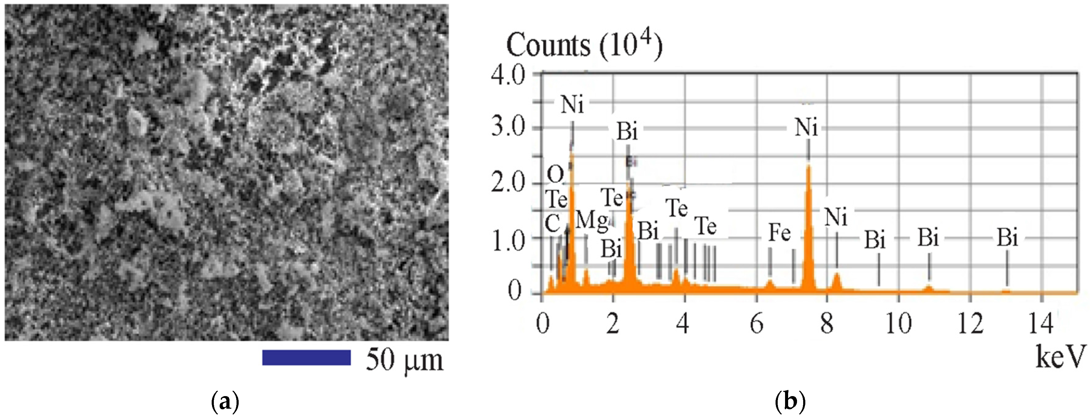
| Composition | Element | ||||||
|---|---|---|---|---|---|---|---|
| Bi | Te | Ni | Fe | C | O | Mg | |
| wt % | 24.87 | 5.15 | 50.13 | 1.95 | 6.57 | 5.63 | 5.70 |
| at % | 5.46 | 1.85 | 39.15 | 1.60 | 25.06 | 16.12 | 10.75 |
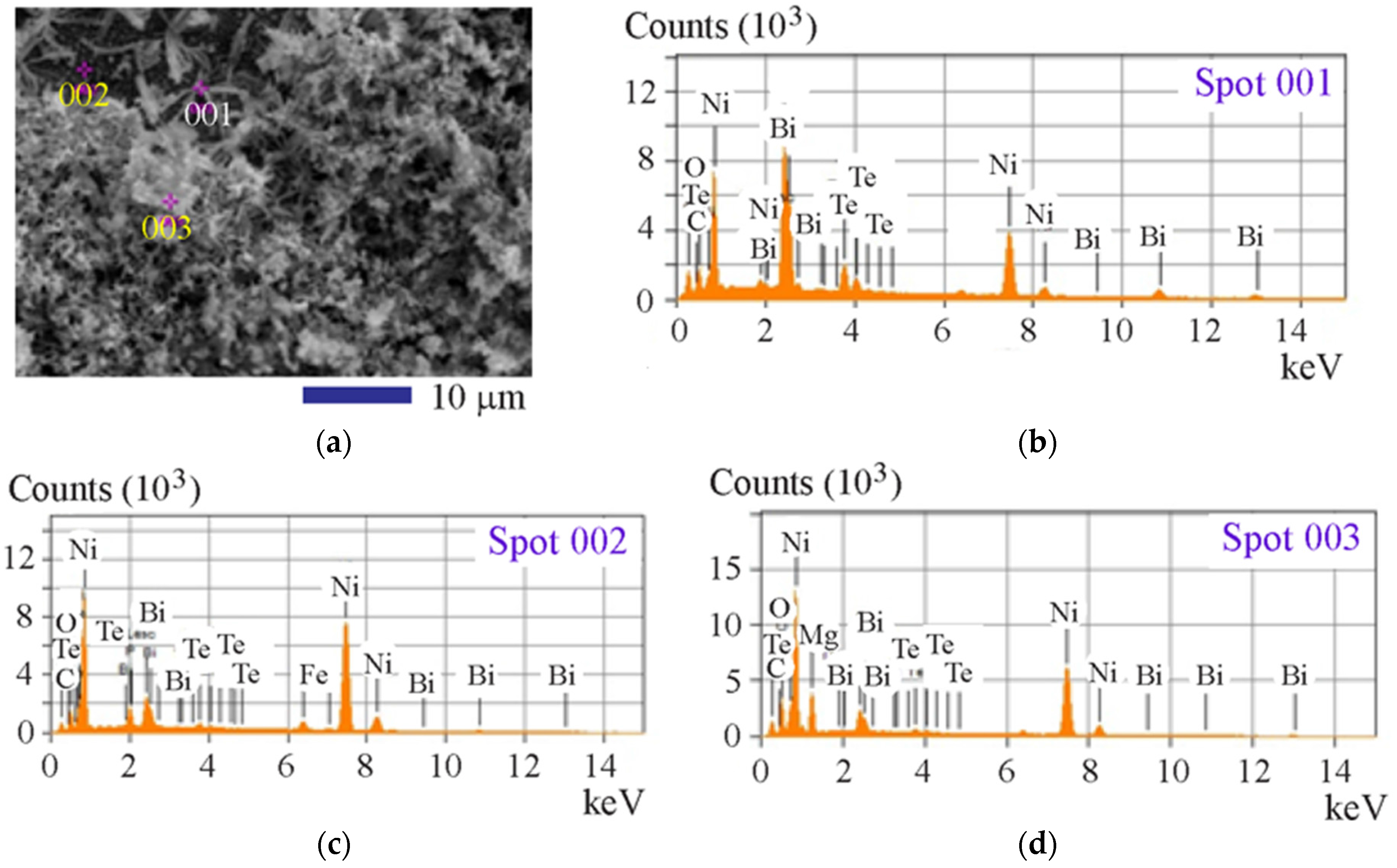
| Element | wt % | |||
|---|---|---|---|---|
| Spot 1 | Spot 2 | Spot 3 | Average | |
| Bi | 44.07 | 12.33 | 9.33 | 21.91 |
| Te | 10.97 | 1.87 | 2.03 | 4.96 |
| Ni | 30.59 | 68.21 | 48.06 | 48.06 |
| Fe | 3.85 | 2.95 | 0 | 2.45 |
| Mg | 0 | 0 | 19.08 | 6.04 |
| O | 10.53 | 5.33 | 10.29 | 8.27 |
| C | 0 | 6.77 | 6.60 | 4.26 |
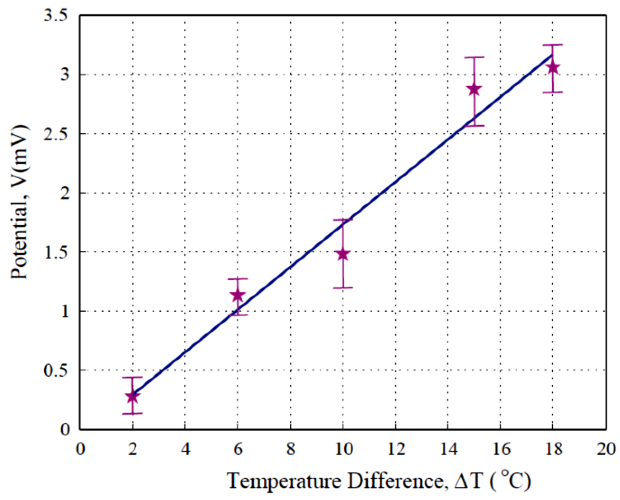
| Temperature Difference (°C) | Voltage (mV) |
|---|---|
| 2 | 0.2797 |
| 6 | 1.1350 |
| 10 | 1.4843 |
| 15 | 2.8284 |
| 18 | 3.0625 |
© 2017 by the authors. Licensee MDPI, Basel, Switzerland. This article is an open access article distributed under the terms and conditions of the Creative Commons Attribution (CC BY) license (http://creativecommons.org/licenses/by/4.0/).
Share and Cite
Gan, Y.X.; Hamdan, A.S.; Gan, J.B.; Li, M. Chemical Vapor Deposition of Bi-Te-Ni-Fe on Magnesium Oxide Substrate and Its Seebeck Effect. Coatings 2017, 7, 164. https://doi.org/10.3390/coatings7100164
Gan YX, Hamdan AS, Gan JB, Li M. Chemical Vapor Deposition of Bi-Te-Ni-Fe on Magnesium Oxide Substrate and Its Seebeck Effect. Coatings. 2017; 7(10):164. https://doi.org/10.3390/coatings7100164
Chicago/Turabian StyleGan, Yong X., Anan S. Hamdan, Jeremy B. Gan, and Mingheng Li. 2017. "Chemical Vapor Deposition of Bi-Te-Ni-Fe on Magnesium Oxide Substrate and Its Seebeck Effect" Coatings 7, no. 10: 164. https://doi.org/10.3390/coatings7100164
APA StyleGan, Y. X., Hamdan, A. S., Gan, J. B., & Li, M. (2017). Chemical Vapor Deposition of Bi-Te-Ni-Fe on Magnesium Oxide Substrate and Its Seebeck Effect. Coatings, 7(10), 164. https://doi.org/10.3390/coatings7100164