Review

Spray-on Thin Film PV Solar Cells: Advances, Potentials and Challenges

University of Michigan-Shanghai Jiao Tong University Joint Institute, Shanghai 200240, China
Coatings 2014, 4(1), 60-84; https://doi.org/10.3390/coatings4010060
Submission received: 6 December 2013 / Revised: 3 January 2014 / Accepted: 8 January 2014 / Published: 21 January 2014
(This article belongs to the Special Issue Novel Thin Film Materials for Photovoltaic Applications)

Abstract

:
The capability to fabricate photovoltaic (PV) solar cells on a large scale and at a competitive price is a milestone waiting to be achieved. Currently, such a fabrication method is lacking because the effective methods are either difficult to scale up or expensive due to the necessity for fabrication in a vacuum environment. Nevertheless, for a class of thin film solar cells, in which the solar cell materials can be processed in a solution, up scalable and vacuum-free fabrication techniques can be envisioned. In this context, all or some layers of polymer, dye-sensitized, quantum dot, and copper indium gallium selenide thin film solar cells illustrate some examples that may be processed in solution. The solution-processed materials may be transferred to the substrate by atomizing the solution and carrying the spray droplets to the substrate, a process that will form a thin film after evaporation of the solvent. Spray coating is performed at atmospheric pressure using low cost equipment with a roll-to-roll process capability, making it an attractive fabrication technique, provided that fairly uniform layers with high charge carrier separation and transport capability can be made. In this paper, the feasibility, the recent advances and challenges of fabricating spray-on thin film solar cells, the dynamics of spray and droplet impaction on the substrate, the photo-induced electron transfer in spray-on solar cells, the challenges on characterization and simulation, and the commercialization status of spray-on solar cells are discussed.

1. Introduction

Paradoxically solar radiation is an endless source of free energy to planet earth and could provide the entire current global energy needs even if used in partial capacity. To make that happen, vigorous research and development activities are being undertaken through spin-off companies, state-funded or university laboratories, or R&D divisions of companies in the energy or high-tech sectors.
The photovoltaic effect, i.e., creation of voltage or electric current in a material upon exposure to light, was first used in specialty applications in the form of crystalline semiconductor silicon or similar solar panels. This was achieved by exploiting the existing semiconductor technology. Silicon is the second most abundant element in the earth’s crust (27.7 wt%), but it is in the amorphous form. High purity crystalline silicon or other semiconductors are required for crystalline solar cells making them relatively expensive to manufacture. The cost-benefit ratio is the most determining factor and driving force in any industry. Due to the high cost of the crystalline silicon and the vacuum-based fabrication process of such solar cells, research and development have also been directed towards the invention and development of alternative solutions, such as various forms of thin film and emerging PV solar cells. A recent decline in the global cost of silicon has challenged the need of emerging thin film solar cells in their infancy; nevertheless, all alternatives are still viable since none of the existing technologies is economically dominant. Each of the existing technologies suffers from one or more major deficiencies, from the lack of sufficient raw materials, to being environmentally toxic, or because of the insufficient cell efficiency, lack of stability or durability or lack of a cost-effective technique to fabricate them.
Two major challenges and concerns in thin film solar cell research are as follows: one is to synthesize suitable, stable, environmentally-friendly and durable solar cell materials that can effectively convert a large portion of the incident solar radiation into separated charges and the second challenge is to devise a practical manufacturing technique to convert the solar cell materials into solar panels. The focus of this paper is on the latter.
As mentioned above, crystalline silicon solar cells are the first generation of solar cells and are currently the major game player in the field, as far as commercialization and current sales are concerned. Solar cells of the second generation, such as copper indium gallium selenide (CIGS) and cadmium telluride (CdTe) need fewer raw materials, but are still costly and usually need special equipment and energy consuming processes such as vapor deposition for their production. The third generation of solar cells (polymeric, organic, quantum dot and dye-sensitized solar cells) has emerged in the last decade or so with the hope of enabling the fabrication of large area panels using less-complex processes and less-expensive materials and equipment. However, they still suffer from low efficiencies, instability, and insufficient durability. The third generation solar cells, instead of expensive semiconductors, usually employ solution-processed molecular semiconductors such as polymers, nanoparticles, quantum dots and additives making them easier to manufacture using economical methods and processes.
The current methods employed for fabricating solution-processed solar cells are usually some sort of casting method such as spin-coating and doctor-blading suitable for lab scale fabrication, and up scalable techniques such as screen printing, slot-die coating, gravure printing, ink jet printing and spray coating [1,2,3]. Wengeler et al. [3] compared large area coating methods for polymer solar cells including knife-over edge coating, slot-die coating, and spray coating with the spin coating method. As expected, their results indicated that the coating method itself has an impact on the film morphology, density, roughness, structure and consequently on the opto-electrical properties. The effect of shearing blade coating on the morphology of organic thin films has also been studied using an in situ technique enabling study of the crystal growth [4]. Among the above-mentioned methods, spray coating is believed to have the potential to produce thin films in a roll-to-roll and high throughput process. The film integrity, internal structure, morphology and effective photon to electron conversion are still issues remaining to be unraveled. Ink-jet printing is a high precision and high resolution technique, but compared to spray coating it is a slower process. It appears that ink-jet printing is more suitable for the fabrication of lines and grids such as electrodes [5] rather than the entire surface area of the active layer of a solar cell, for instance.
Spray coating is a multi-step method, comprising several steps such as atomization of a liquid solution or mixture, droplet flight and evaporation, droplet impact on the substrate, droplet spreading, receding, recoiling, drying, solute adhesion and bonding to itself and to the substrate. To obtain a high quality and acceptable spray-coated layer, all of these processes have to be well understood and controlled. Parallel or post processing may be also helpful.
In the rest of this paper, recent advances on the fabrication of polymer, dye-sensitized, quantum dot and other solution processed solar cells are presented. Then the dynamics of spray droplet impact on a substrate, droplet spreading and drying in the formation of a thin film is discussed. The effect of spraying on photo-electron charge dissociation and transfer, simulation of the spray coating process, some characterization techniques and finally the status of commercialization of spray-on PV solar cells are elucidated.

2. Recent Advances

Based on current knowledge, the application of spray coating is limited to solution-processed solar materials. Spray coating is not the right method for the formation of dense, highly ordered and uniform or crystalline layers such as inorganic semiconductors, although, it may be used to form structured organic layers, e.g., [4].

2.1. Polymer Solar Cells

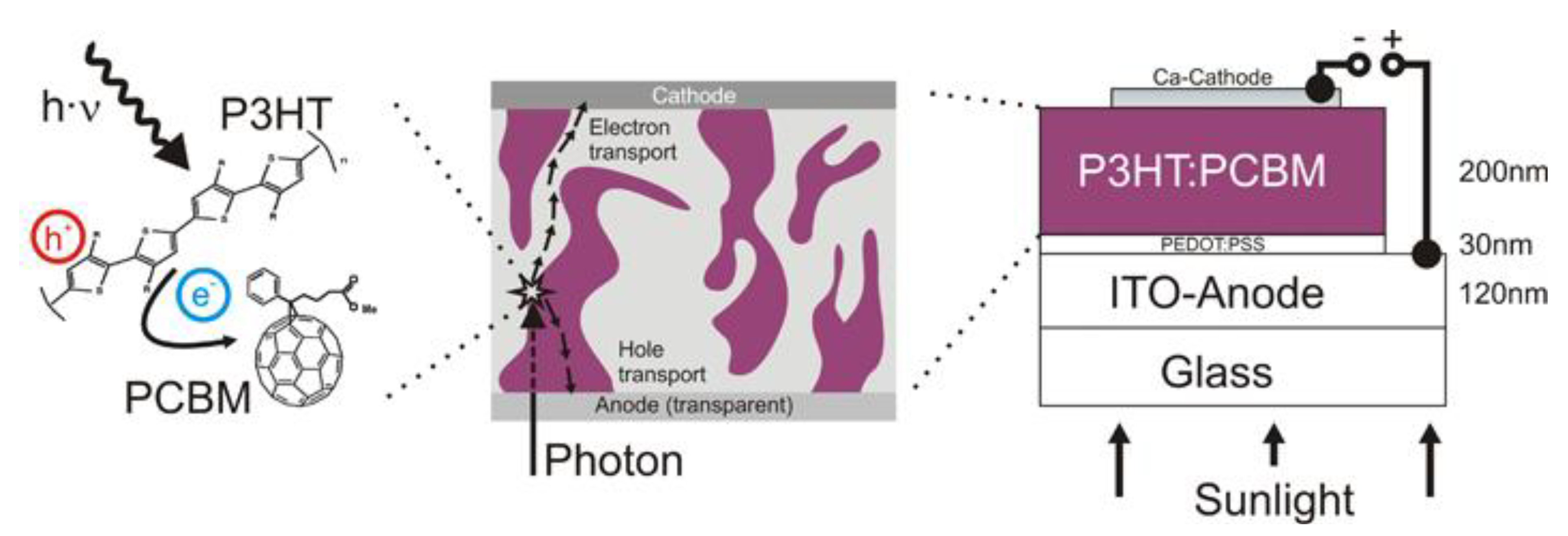
2.1.1. Principle of Operation

An important class of thin film solar cells that can be fabricated almost entirely via spray coating is the polymer solar cell. In a polymer solar cell, an active layer is sandwiched between two collecting electrodes. One of the electrodes must be transparent to allow transmission of solar radiation to the active layer. Currently indium tin oxide (ITO) is the widely used transparent conductive layer, which is deposited on glass substrates by sputtering. As the second electrode, silver, aluminum and other metals that have the right work function are usually thermally evaporated on the solar cell layers to complete the device [1]. The active layer is comprised of an electron donor and an electron acceptor. The common and currently used approach is to blend the donor and acceptor material in solution, transfer the solution to the substrate, and let the solvent evaporate to leave behind a thin film.
Once photons strike on the solar cell surface and reach the active layer, the polymer molecule becomes excited and a so-called exciton forms. The exciton diffuses to the boundaries of the donor-acceptor blend where it dissociates to an electron and a hole due to a change in the energy level of the two materials. The electrons and holes then transfer to the opposite electrodes under the influence of different work functions of the electrodes. To minimize charge recombination, intermediate or buffer layers may be used between the electrodes and the active layer to block the electron or hole transfer in the wrong direction. Some examples of hole transport buffer layers include PEDOT:PSS or poly(3,4-ethylenedioxythiophene) poly(styrenesulfonate), V2O5 and MoO3. Electron transfer buffer layers are in the form of metal oxides such as TiO2 and ZnO ceramic thin films. A blend of poly(3-hexylthiophene) (P3HT), a polymer, and [6,6]-phenyl C61-butyric acid methylester (PCBM), a fullerene derivative based donor-acceptor molecule, is one of the most widely used organic solar cell materials for photon to electron conversion. It is not the most efficient polymer blend, but the most studied. Organic polymers such as P3HT:PCBM blends have wider band gaps than natural semiconductors. Thus they have an efficient absorption at the near UV portion of the spectrum. The band gap of the polymer solar cells can be altered and tuned by changing the ratio of their constituents and also by the arrangement and alignment of the molecules [6].
Most layers of polymer solar cells are solution-processed and therefore compatible with spray coating. One challenge here is the formation of the various thin layers stacked on top of one another. An issue with the traditional device, shown in Figure 1, is that the deposition of P3HT-PCBT on PEDOT:PSS may not create adequate bonds. Alternatively, using an inverted device, PEDOT:PSS may be deposited on top of the P3HT:PCBT layer.
Figure 1. Layer structure of a conventional polymer solar cell [7]. P3HT: poly(3-hexylthiophene); PCBM: [6,6]-phenyl C61-butyric acid methylester; ITO: Indium Tin Oxide; PEDOT:PSS: poly(3,4-ethylenedioxythiophene) poly(styrenesulfonate).
Coatings 04 00060 g001

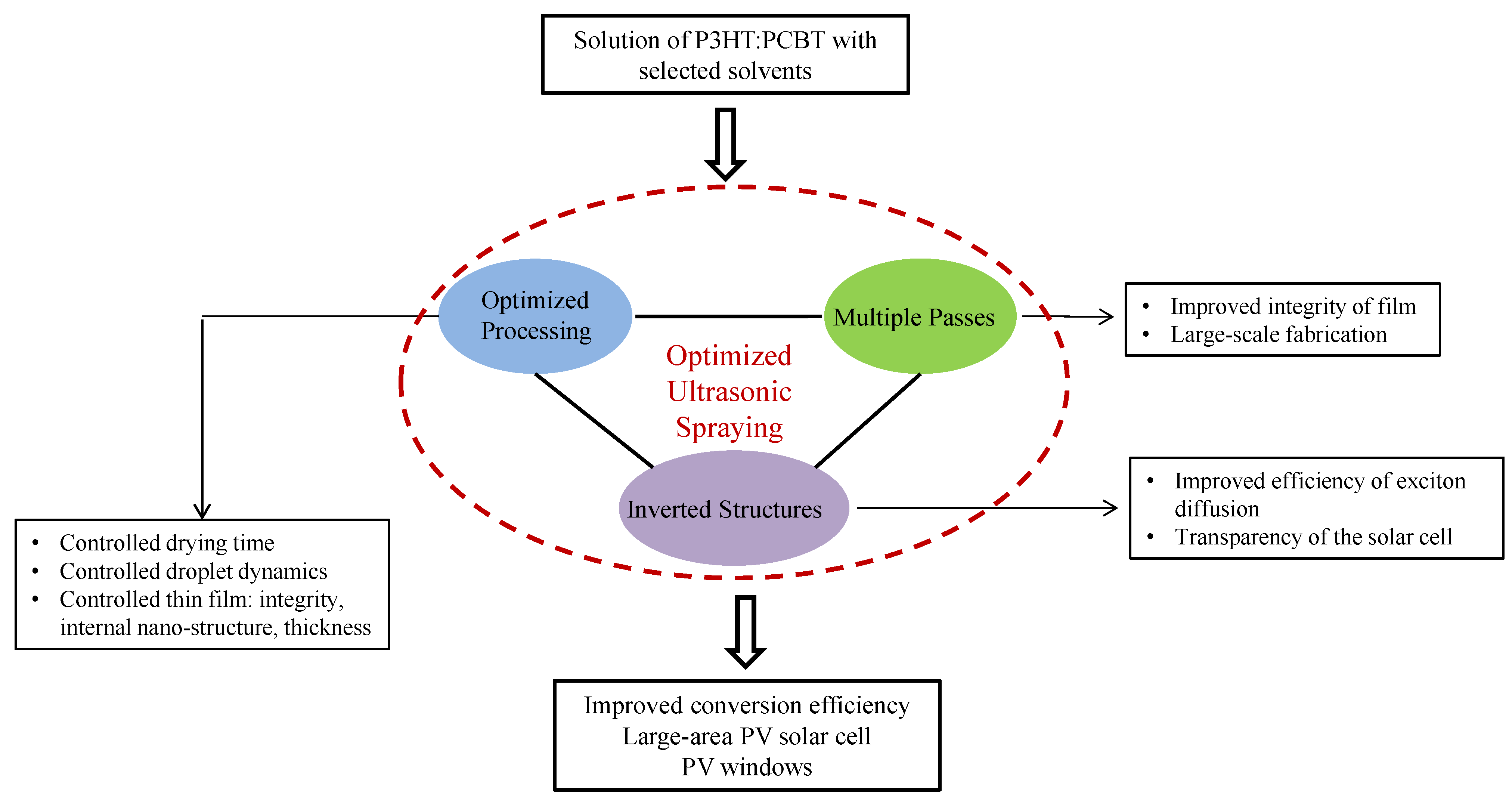
2.1.2. Recent Advances on Spray-on Polymer Solar Cells

The electron blocking PEDOT:PSS layer, which could also function as the anode in an inverted configuration, has been fabricated by spray coating and studied rather well [8,9,10,11,12,13,14,15,16,17,18]. The objective of those studies has been to improve the performance of the layer by adjusting the processing parameters. For instance, application of spray coating on a semi-wet brush-coated PEDOT:PSS layer was shown to provide fairly uniform layers [8]. The setback, however, is that this is not a one step process thus removing the main advantage of spray coating as a fast process with roll-to-roll capability. Spray-on PEDOT:PSS layers may also be modified by adding selected solvents and also by post annealing to improve their conductivity and structure [9].
In an attempt to reduce or eliminate the defects such as pinholes and non-uniformities, Lee et al. [12,13] studied the effect of annealing and also the effect of using various solvents for spray coating of P3HT:PCBM layer on PEDOT:PSS using a gas-assist nozzle (air brush). It was found that additional spraying of ortho-dichlorobenzene (DCB) solvent after the conventional spray coating process of P3HT:PCBM improves all physical, optical and electronic characteristics of the film. In a study, a cell consisting of four layers including ITO–Cs2CO3–(P3HT:PCBM)–modified PEDPT:PSS, was formed on a glass substrate. The encapsulated solar array showed more than 30% transmission in the visible-near IR range and an increase in the photo conversion efficiency in the annealed samples was reported. Ultrasonic atomization is a more sophisticated atomization technique compared to airbrush and has been extensively used to fabricate PEDOT:PSS and P3HT:PCBM layers, e.g., [15,16,17,18]. In one study, the application of concurrent spray coating was investigated where two independent solutions were coaxially pumped to the ultrasonic nozzle, each consisting of one of the two respective solutions. By changing the flow rate of these two solutions, some of the process parameters were readily altered. It was observed that the two solutions remained predominantly separate from each other until they mix and coalesce on the substrate. Chen et al. [19] used a similar approach in which P3HT and PCBM were sprayed through two nozzles. This was done to control the domain formation and phase separation in the active layer. The morphology of the donor-acceptor active layer domain has a great influence on the charge formation, separation and transfer to the electrodes.
It has been demonstrated that by using PEDOT:PSS highly diluted with low surface tension solvents such as isopropyl alcohol and butanol, a relatively uniform thin layer can be achieved on the P3HT:PCBM layer (using an airbrush). This is due to the improved wettability of P3HT:PCBM with respect to PEDOT:PSS [20]. Two major droplet properties that control the droplet spreading and therefore the film integrity are the surface tension and viscosity. Reducing the surface tension can facilitate droplet spreading. Electrospray deposition has been also used to fabricate polymer solar cell layers [21,22]. A solvent effect was observed when different organic solvents were used. Also, electrohydrodynamic atomization (similar to electrospraying) technique has been used to fabricate PEDOT:PSS thin films [23]. The modes of atomization and their effect on the film morphology were studied. Spray coating via electrohydrodynamic atomization was also employed to fabricate zinc oxide and titanium oxide thin films, which can be used for electron transfer buffer layers, electrodes, etc. [24,25]. Attempts have been made to fabricate spray-on electrodes as well. For instance, Hau et al. [26] spray coated silver nanoparticles to form the anode in an inverted device. The device performance was improved when multiple spray passes were used; however, the performance was still low compared to the evaporated silver electrodes. Other materials such as PEDOT:PSS, carbon nanotubes and graphene have the potential to be used for electrodes as well [27]. Single-walled carbon nanotube films [28] and silver nanowires [29] have been fabricated by spray coating. In a recent work, the influence of rheological properties on spectral selectivity during spray coating of thickness insensitive spectrally selective paint coatings was examined [30].
A simple set of equations that can be used to estimate drying time and film thickness in ultrasonic spray deposition of solution processed solar cells, are given in this reference [31]. Investigations of the effect of spray characteristics on the morphology of spray coated layers have been conducted but the results are not yet conclusive [32,33]. Lonakar et al. [33] studied the effect of spray flow rate and droplet size on device performance and established a correlation between process parameters and the film formation process, such as the time to cover the coated area by droplets and the time for droplet evaporation.
The efficiency of large area solar cells is usually smaller than those with small areas. Spray coating has been used to fabricate solar cells of 12.25 cm2 area with a power conversion efficiency of 2.11% [34]. Recently, a P3HT:PCBM layer of modules up to 25 cm2 was fabricated by a specific surface treatment, based on the deposition of a fluorinated self-assembled monolayer on top of the bottom electric contact [35]. It is noteworthy that the number of publications in the area of spray-on solar cells has increased exponentially in the past few years indicating the feasibility and potential of this process. Additional related works may be found in Refs. [36,37,38,39,40,41,42,43,44,45].

2.2. Dye-Sensitized Solar Cells (DSSCs)

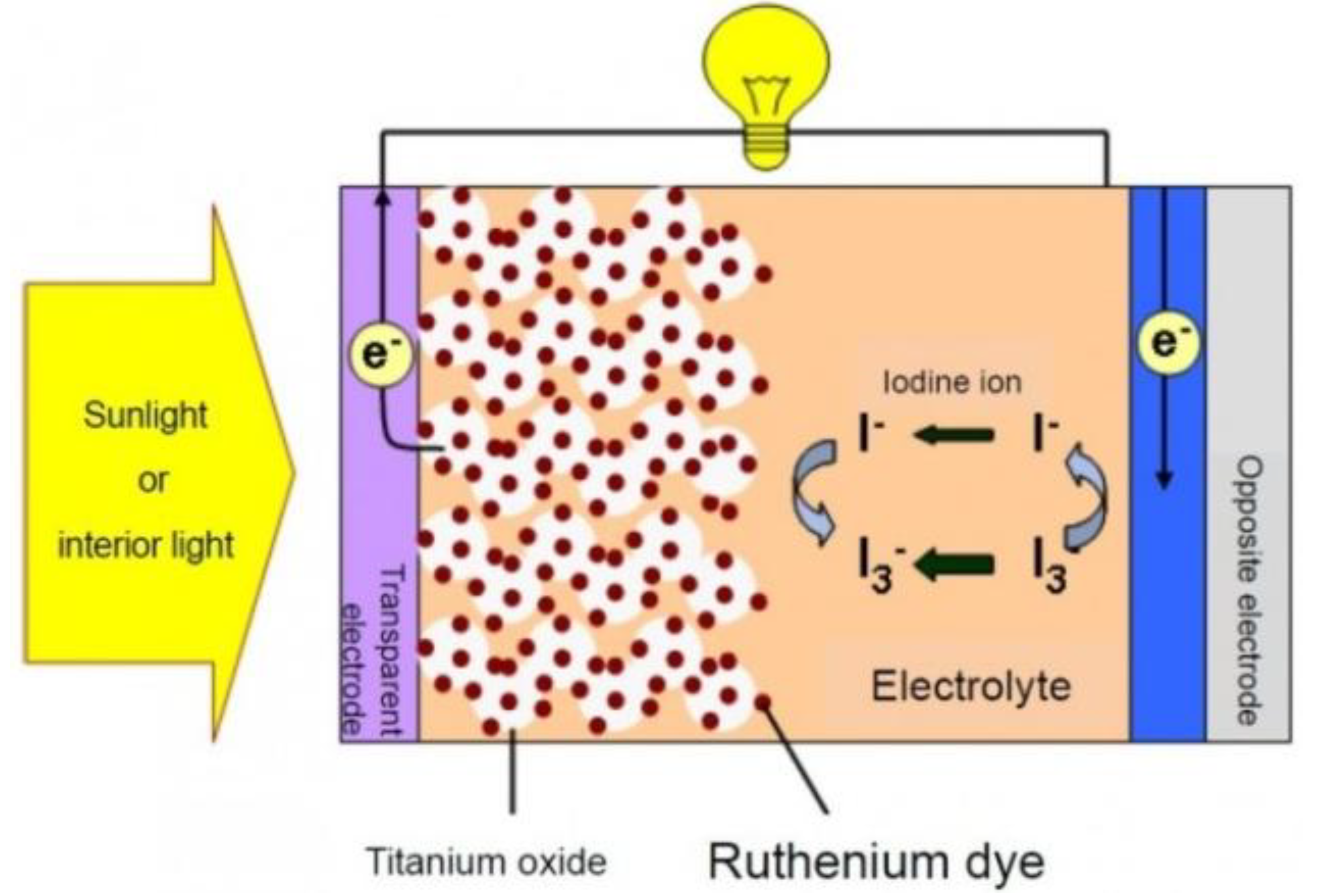
2.2.1. Principle of Operation of DSSCs

In a traditional DSSC, the main layer is a porous film of TiO2 mesoporous nanoparticles, sensitized by a molecular dye such as ruthenium-polypyridine. The dye molecular structure can be tuned to absorb a wide range of wavelengths in the solar spectrum. To complete the solar cell device, the TiO2 phase is immersed in an electrolyte solution. The TiO2 is the anode and platinum is the cathode of the cell. The anode and cathode are sandwiched between two Transparent Conducting Oxide (TCO) materials or flexible plastic substrates such as polyethylene terephtalate (PET) and sealed. Figure 2 shows the current transfer mechanism in a typical DSSC.
Figure 2. Electron transfer mechanism in a dye-sensitized solar cell (DSSC).
Coatings 04 00060 g002
To build a DSSC in the lab, TiO2 paste is transferred to a TCO substrate by doctor balding or a similar method, heated on a hot plate to burn off the additives, and then immersed in a dye solution to absorb the dye on the surface of the TiO2 molecules. The second substrate is then placed on top of the TiO2-dye combination, an electrolyte solution is injected into the substrate, and the cell is sealed.

2.2.2. Recent Advances on Spray-on DSSCs

For roll-to-roll and large scale fabrication of DSSCs, plastic substrates are more convenient than TCO coated glass substrates. For such substrates, the thin film TiO2 layer may be fabricated by spray coating of a solution containing TiO2 nanoparticles at a low temperature, since the plastic substrates cannot essentially sustain high temperatures used in the conventional methods [46,47]. In a study [46], TiO2 nanoparticles were deposited on an F-doped tin oxide conducting glass in a vacuum cold spraying process. This resulted in the formation of a porous TiO2 layer. Similarly, the fine dispersion of the commercially available nanocrystalline TiO2 particles in ethanol was electro-sprayed directly onto a fluorine-doped tin-oxide (FTO) substrate [48,49]. This layer was then used to fabricate a complete device. In another work, and in an attempt to achieve a fast production method, the dye was sprayed onto an existing TiO2 coated substrate, rather than using the conventional immersion technique [50].
The porous TiO2 thin film can be fabricated by spray pyrolysis technique as well [51]. Spray pyrolysis is a version of spray coating but needs a higher substrate temperature to assure the occurrence of the chemical decomposition of the liquid precursor needed to form a ceramic thin film plus some volatile gases. Titanium (IV)oxy acetylacetonate 2-butanol solution may be used as the starting precursor for the fabrication of TiO2 thin films with a substrate temperature of about 300 °C [51]. Also, Nb2O5 produced by spray pyrolysis may be used as the counter electrode in a DSSC [52]. Transparent conducting Li-doped NiO thin films [53] and water-soluble polyelectrolyte-grafted multi-walled carbon nanotube films [54] are the other layers that may be fabricated by spray pyrolysis.

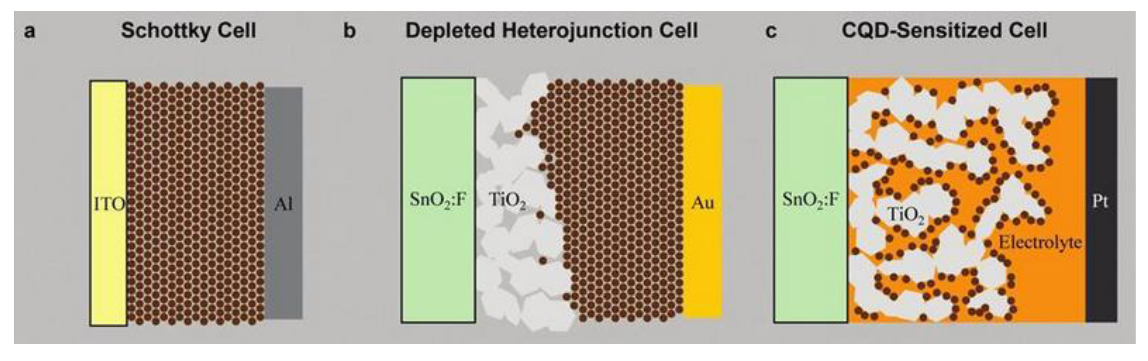
2.3. Quantum Dot Solar Cells (QDSC)

2.3.1. Principle of Operation

Quantum dots (QDs), also known as nanocrystalline or nanocrystal semiconductors may function as sensitizers to enhance light absorption in some solar cells or as main electron donor agents in some other cells. QDs may be used in solar cells in the following forms. In the first form, QDs are used in solid state films to act as inter-band dopants. These solar cells need expensive vacuum equipment to manufacture. The second configuration is similar to the DSSCs in that QDs act like sensitizing dyes. The third configuration is the organic QD hybrid solar cells, wherein QDs are blended with an organic semiconductor material such as a polymer. The photo-generated excitons in the QD are separated at the interface with the polymer forming electrons and holes. A fourth design has been introduced as well called the Schottky-quantum dot and depleted heterojunction solar cell, which may be processed in solution [55]. The last type has an ITO/PbS QD film/Al structure in which the QDs form a Schottky contact with the Al electrode to create a depletion layer to aid with exciton dissociation. The other intermediate layers may be added to improve the conversion efficiency. Some examples of QD solar cells are shown in Figure 3.
Figure 3. Three quantum dot (QD) solar cell architectures [56].
Coatings 04 00060 g003

2.3.2. Recent Advances on Spray-on QDSCs

Colloidal and solution processed QD solar cells can be readily fabricated by spray coating [57,58]. For instance, in Ref. [58] two spray nozzles were used to transport droplets of two different precursors, one containing the QDs and the other containing the polymer to deposit QD/Polymer hybrid structures. The photo-current experiments of QD/polymer hybrid composites showed evidence of enhanced carrier generation and transport as a result of intimate contact between QDs and polymer molecules.

2.4. Other Thin Film Solar Cells

Hydrogenated amorphous silicon (a-Si:H or more commonly a-Si) p-i-n solar cells are usually deposited using plasma enhanced chemical vapor deposition (PECVD), where a significant percentage of the hydrogen atoms are bonded into the amorphous silicon structure. Spray coating does not seem to be the right method for the fabrication of the Si layers, however, it has been employed to synthesize their electrodes, such as ZnO:In layers [59], transparent conductive F-doped SnO2 [60], In-doped ZnO [61], Al-doped ZnO and F-doped SnO2 [62] thin films.
In cadmium telluride thin film solar cells, a layer of cadmium sulphide is deposited from solution onto a glass sheet coated with a transparent conducting layer. This is followed by the deposition of the main cadmium telluride layer by as variety of techniques including close-spaced sublimation, vapor transport, chemical spraying, or electroplating. Large-area CdS/CdTe solar cells have been made by spraying of CdTe onto the surface of CdS/SnO/glass structures, followed by heat treatment. This is regarded as a low-cost technique amenable to continuous processing and automation [63].
Copper Indium Gallium Selenide Solar Cell (CIGS) has the formula of CuInxGa(1−x)Se2, where the value of x can vary from 1 (pure copper indium selenide) to 0 (pure copper gallium selenide). The CIGS thin film solar cells have a high efficiency among thin film solar cells. The conventional manufacturing technique is based on the vacuum co-evaporation, in which Cu, In and Ga are sequentially co-evaporated and selenized. In recent years, non-vacuum and low cost methods have been practiced as well [64]. Some of these methods include electro, electro-less and chemical bath deposition, and solution-processed methods such as spraying or spin coating [65,66]. Using the last approach, Schulz et al. [66] used a low temperature colloidal route to make CIGS solar cells. Their device showed an efficiency of 4.6%. In a study, all layers of a CIGS cell were fabricated by a spray method [67]. The Zn0.76Mg0.24O layers were used as buffer layers in thin film solar cells with the configuration, glass/Mo/CuIn0.8Ga0.2Se2/Zn0.76Mg0.24O/ZnO:Ga/Cu–Au using sprayed p-CuIn0.8Ga0.2Se2 (CIGS) as an absorber layer and sprayed n-ZnO:Ga as a window layer. This is a CdS-free vacuum-free CIGS solar cell. As another example of CdS-free CIGS cell, solar cells by an alternative material, InxSy thin film buffer layers were prepared by ultrasonic spray pyrolysis [68]. In Ref. [69], current fabrication techniques and their potential including spray deposition are discussed. Others have also fabricated layers of CIGS solar cells by spray coating, e.g., [70,71,72,73].

3. Dynamics of Droplet Impact on a Dry Surface

Impaction of a droplet on a dry solid surface could be different from that on a liquid surface or a wet surface, although many similarities exist between these two processes. In spray-on solar cell fabrication process, droplets may impact on a dry substrate or on a thin film of liquid or wet lamellae already formed on the substrate as a result of the impaction of the earlier droplets. These two combined effects complicate the process further. Here for simplicity, it is assumed that the droplets impact on a hot dry surface, an assumption which is justified if the impacted droplets rapidly dry or the residual solvent only slightly wets the surface.

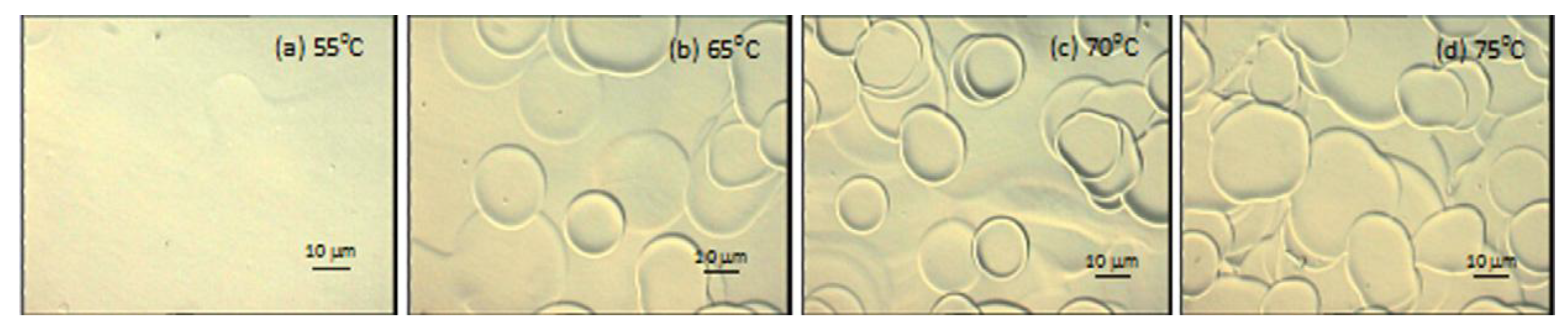
3.1. Droplet Impact on a Cold Surface

The process of spray droplet impacting a solid surface is characterized by the droplet Weber (We), Reynolds (Re), Ohnesorge (Oh), and K numbers, as well as surface roughness and wettability. Upon impact, processes such as spreading, receding, rebounding, splashing, coalescing, and drying may occur. Under given processing conditions, some of the above-mentioned processes may be absent. The initial impact and spreading characteristics form the foundation of a coating layer. An air bubble may be entrapped inside the droplet upon impact. This may affect the film integrity and the operation of the solar cell. The desired case for solar cell fabrication and other coating processes is the deposition mode, which requires a low or moderate droplet impact velocity. The ratio of the final lamella diameter at the wall to that of the droplet ranges from approximately 1.25 to 5 for different droplet impacts resulting in deposition without recoil. This ratio is proportional to the droplet We number and inversely proportional to the Oh number [74,75]. An increase in droplet density, diameter and impact velocity and a decrease in surface tension and viscosity favor the formation of a larger and thinner lamella. The kinetic energy of the impacting drop is partly dissipated by the viscous forces and partly converted into the surface energy associated with the greatly increased free-surface area of the lamella. The subsequent behavior of the lamella depends largely on the surface wettability, which is related to the contact angles. For the fabrication of spray-on solar cells, it is desirable to have very small contact angles.
Parameters that affect the deposition characteristics include the droplet impact velocity, diameter, density, surface tension and viscosity. In terms of the non-dimensional numbers, if We½ Re¼ is smaller than 57.7, the droplet will be in the deposition mode and splashing will be avoided. An increase in the impact velocity, droplet diameter and density, and a decrease in viscosity and surface tension facilitate the occurrence of the splashing mode. In other words, the same effects that result in a thinner lamella and a better spreading (increase in density, diameter and impact velocity, and a decrease in surface tension and viscosity) also result in an increase in the likelihood of splashing, even though their functionality is not the same. What is also important is the roughness and wettability of the surface, which has not been considered in the foregoing criterion. For instance, an increase in the surface roughness increases the onset of splashing [74].
In polymer solar cells, a blend of a polymer and large fullerene derivative molecules are dissolved in chlorobenzene or a similar solvent to make the active layer. The concentration of the solution droplets is low, the evaporation rate of the solvent is also low during the droplet flight and therefore it can be safely assumed that the solution droplet impact is not affected by the solute [5,31]. For 40 µm droplets of solvent chlorobenzene at 50 °C with an impact velocity of 10 m/s, the dimensionless term introduced above for the onset of splashing, viz., We½ Re¼ is about 64, which is slightly higher than the splashing threshold. A velocity of 10 m/s is quite high for spray coating of solar cell materials and lower velocities are recommended. For instance, the velocity of the droplets produced by ultrasonic atomization can be controlled by the velocity of the carrier gas [5]. For an impact velocity of 3 m/s, the above dimensionless group will be about 14, which is well below the splashing threshold. The surface texture, however, may significantly affect the above splashing threshold.

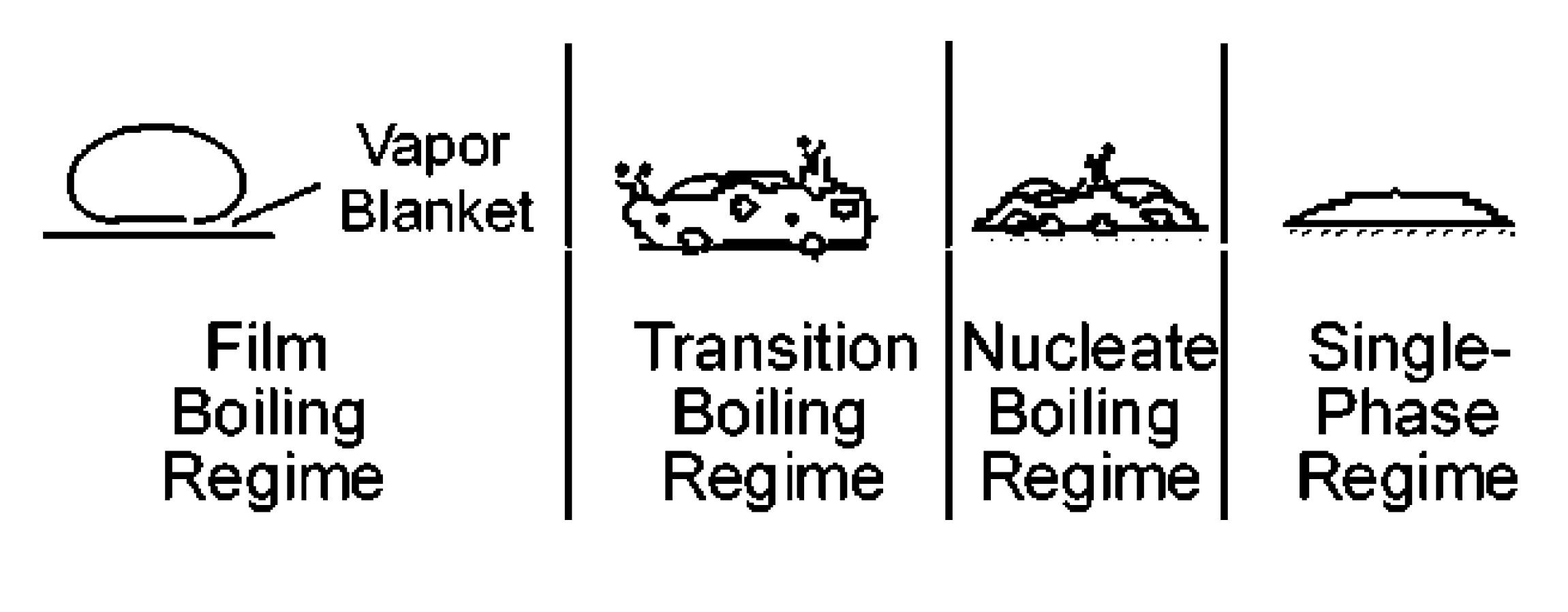
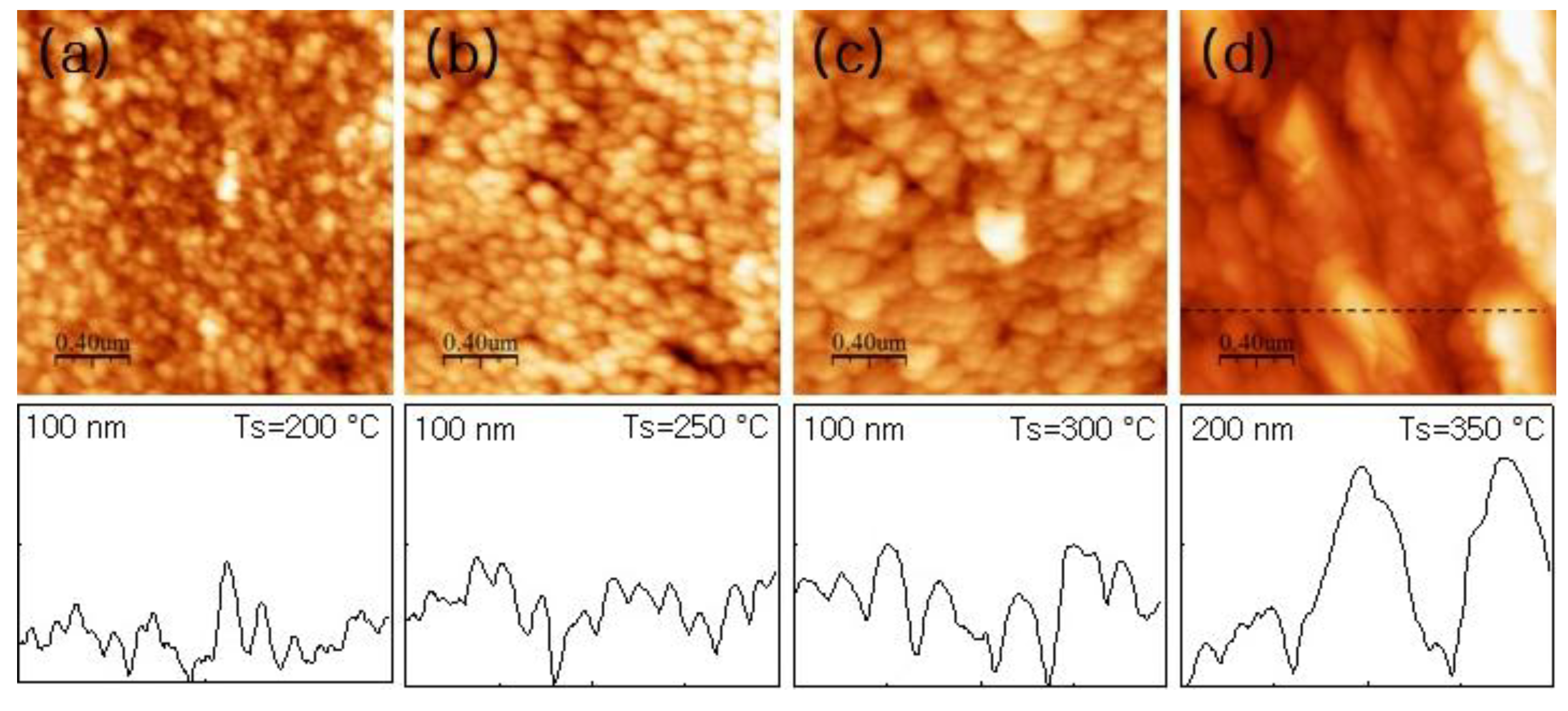
3.2. Droplet Impact on a Hot Surface

Droplet impact dynamics on a cold surface discussed in the previous section may be different from droplet impact dynamics on a hot surface, particularly if the surface temperature is higher than the liquid boiling point, which is the case in some spray coating processes such as spray pyrolysis.
Depending on the surface temperature, also surface texture, several scenarios may occur upon droplet impact. At sufficiently high temperatures, the evaporation mode is the film boiling regime in which the droplet-solid contact is minimized by the rapid formation of vapor layer at the interface (Figure 4). As a result, the droplets appear to shatter and bounce off the solid surface upon impact. The lower temperature boundary of this regime is called the Leidenfrost point, which also corresponds to the minimum heat transfer rate from the surface. As surface temperatures drop below the Leidenfrost point, a transition boiling regime is encountered, where the droplet-solid contact is prolonged, the droplet dynamics changes and the heat transfer rate increases. At lower temperatures, the nucleate boiling regime prevails where complete wetting of the surface occurs and the heat transfer rate is the maximum. Nucleate boiling results in the formation of cavities, affecting droplet deposition. At the bottom end of the nucleate boiling regime, boiling ceases and a single-phase heat transfer regime is encountered, where heat transfer is dominated by single-phase convection [76]. Figure 4 schematically shows the above-mentioned five regimes, as far as droplet dynamics is concerned. Therefore, only in the single-phase regime, is the dynamics of droplet impact on a heated surface similar to that of a cold surface.
Figure 4. Droplet impact behavior in droplet-heated surface interaction. Photo reprinted from Ref. [76] with permission from ASME.
Coatings 04 00060 g004
The Leidenfrost temperature, which is the onset of film boiling, is a function of the liquid physical properties as well as surface texture [77]. For water, methanol, and ethanol on various surfaces it ranges from 150 to 200 °C. The quantitative history and fate of a water droplet impinging on a heated substrate has been obtained and shown in Ref. [78]. For instance, it has been shown that the water droplet impact (at We = 20) on a heated surface at two temperatures of 130 and 280 °C (below and above the Leidenfrost point of water) are totally different. At 130 °C, an impinging droplet first spreads, then undergoes nucleate boiling, bubble nucleation, and thin film evaporation at the end. At 280 °C, first a droplet contacts with the surface, followed by rapid formation of a vapor film which results in droplet rebound and bouncing.
The above description of evaporation modes reveals the importance of surface temperature on both the film drying time and also the film texture, homogeneity and integrity. When the solar cell materials are sprayed onto a heated substrate, the surface temperature may rapidly decline after impingement of the first few spray droplets resulting in a change in the evaporation mode. This is more probable if multiple passes of spray coating are deployed, resulting in a varying surface temperature. This may further complicate the prediction of the film morphology. To examine the existence of a correlation between the droplet heat transfer mode at heated surfaces and the film morphology, several spray pyrolysis films produced at various temperatures were examined (Figure 5 and Figure 6). Figure 5 shows the Atomic Force Microscope (AFM) images and line profiles of In2S3 nano thin films produced by spray pyrolysis at various temperatures, all above the Leidenfrost temperature, which is associated with the formation of a vapor film on the surface [79]. The main solvent is water. With an increase in the temperature and therefore increase in the thickness of the vapor film, the droplet impact is further interrupted and the surface roughness increases.
Figure 5. Atomic Force Microscope (AFM) images and line profiles of In2S3 films made at substrate temperature of (a) 200 °C; (b) 250 °C; (c) 300 °C; and (d) 350 °C [79].
Coatings 04 00060 g005
Figure 6. Scanning Electron Microscope (SEM) images of Cu2ZnSnS4 thin films prepared by spray pyrolysis at substrate temperature of 320 °C. Photo reprinted from Ref. [80] with permission from Elsevier.
Coatings 04 00060 g006
Figure 6 shows a Scanning Electron Microscope (SEM) image of the Cu2ZnSnS4 thin film prepared by spray pyrolysis at substrate temperature of 320 °C [80]. The main solvent in this case is methanol. As the images suggests, the film is rough and looks more like a population of particles sticking on a surface rather than forming a film. This is because at high substrate temperatures, impinging droplets recoil and bounce, perhaps several times, and shrink substantially before they actually deposit on the surface.
At substrate temperatures lower than the droplet boiling point, the heat transfer is in the single phase mode and the film morphology is expected to be less-affected or only slightly affected by the surface heating. In polymer or organic thin film solar cells, a review of the literature shows that the substrate temperatures used are usually low, in most cases below the solvent boiling point, or slightly higher, and then to improve the film integrity and texture, spray-on samples are post annealed. In contrast to thin films made by spray pyrolysis, which have a rough and particle like surface, cold spray-on films have a smoother surface (Figure 7). The literature results also show that a lower substrate temperature leads to the formation of a smoother film, e.g., [13,35,36]. Figure 8 and Figure 9 depict this effect. The main reason behind this effect is the delay of solvent evaporation at lower temperatures, which allows the individual droplets to spread and form lamellae that may merge to form an integrated liquid thin film. Gradual evaporation of the solvent leaves behind a rather uniform solid film. If the spray flow rate or the droplet number density is not sufficient to ensure the formation of a liquid thin film, droplets may individually dry upon impact creating a stacked-coin pattern shown in Figure 7. However, spray coating cannot be conducted at room temperature, since a low temperature delays the film drying and settling, which is not favored because it slows down the coating process.
Figure 7. Optical (top) and AFM (bottom) surface profile of P3HT-PCBM in chlorobenzene prepared by spray coating. Photo reprinted from Ref. [12] with permission from Elsevier.
Coatings 04 00060 g007
Figure 8. Optical images of the films deposited by: (a) spin-coating in nitrogen atmosphere; (b) spray-coating in dichlorobenzene; (c) spray-coating in dichlorobenzene:chlorobenzene (DCB:CB) at 25 °C; (d) spray-coating in DCB:CB at 40 °C; (e) spray-coating in DCB:CB at 50 °C and (f) spray-coating in DCB:CB at 70 °C. Photo reprinted from Ref. [35] with permission from Elsevier.
Coatings 04 00060 g008
Figure 9. Optical microscope images of poly(3,4-ethylenedioxythiophene) poly(styrenesulfonate) (PEDOT:PSS) films deposited at four different substrate temperatures shown on each image. Photo reprinted from Ref. [13] with permission from Elsevier.
Coatings 04 00060 g009

3.3. Droplet Interaction

Effect of lateral spacing on the substrate between droplets at the time of impact has been studied in inkjet printing. This is different from the spacing between droplets injected from a fixed nozzle with a time delay. Compared to sprays that cannot produce so reproducible and repeatable droplets, in inkjet printing, droplet trajectory, spacing, and delay can be precisely controlled. Soltman and Subramanian [81] and Kang and Oh [82] experimentally studied the effect of droplet spacing on the characteristics of ink-jet printed lines and investigated the conditions that result in the formation of a smooth line. Teichler et al. [83] studied the effect of several parameters including droplet spacing on the texture, uniformity and homogeneity of polymer films fabricated by ink-jet printing. For 60 µm droplets, a droplet center to center spacing of up to 120 µm resulted in droplet merging and flattening. Further increase in the spacing resulted in the lack of merging.
While it is possible to control droplet spacing in inkjet printing or any other drop-on-demand droplet generation technique [84], precise control of the trajectory of individual droplets in a spray is not possible, because of the transient nature of sprays. Therefore, one strategy to obtain a continuous and integrated solid film is to first form a continuous liquid film on the substrate, i.e., to ensure that the spray droplets impacted on the surface merge and form a liquid thin film before drying. This however requires a low substrate temperature and a low surface tension solvent or solvent group to reduce the droplet contact angle and improve droplet spreading. Marangoni convection may also enhance the extent of droplet spreading. The choice of solvent, surfactant, solution concentration, substrate temperature, and spray flow rate can significantly alter the coating outcome. With precise control of solvent properties, Girotto et al. [16] managed to obtain smooth nanometer sizes of PEDOT:PSS spray-on layers. At higher substrate temperatures typically near and higher than the solvent boiling point, evaporation is rapid and droplets may evaporate rapidly before merging with one another forming isolated stacked-coin or disk-like deposits. Then a multi-pass spray strategy is required to get the entire surface coated. This however, usually results in the formation of uneven films [31].

4. Photo-Induced Electron Transfer

In heterojunction organic/polymer solar cell layers with large domains, conversion efficiency is limited by the number of photo-generated excitons that can be transported to a heterojunction where the excitons may dissociate [85]. After dissociation, the charges need to find their way to the electrodes, or they will be lost due to recombination. Charge carrier diffusion in organic thin films often depends on the layer thickness, texture, internal nano-structure and molecular orientation, available interfaces and pathways for charges to the electrodes all of which may be altered by the fabrication conditions. A change in the orientation and blending of large molecules such as polymers can affect the charge transfer and dissociation, shunt and series resistances, open circuit voltage, short circuit current, fill factor, conversion efficiency and therefore the device performance. One controlling parameter in spray coating is the drying time that affects the structure, texture and morphology of the layers. The slow growth of the active layer in a P3HT-PCBM polymer blend seems to assist the formation of the self-organized and ordered structures in the blend system. The device performance (fill factor and photo-current efficiency) may be deteriorated when the film is dried on a hot plate [86].
The solvent properties also affect the morphology and charge carrier transport of spray-on layers, significantly. At optimum solution conditions, the rough surface of spray-on solar cell layers is not as detrimental as it may look, supported by the fact that the performance of spray-on solar cell devices was comparable to that of smooth-surface doctor-bladed devices [44]. This means that as far as the solution properties are tuned to achieve acceptable inner carrier transfer properties, the high surface roughness associated with spray-on layers can be tolerated. However, note that if the films are ultra-thin and in the nanometer range, a high surface roughness may result in pin-holes and lack of integrity in the film. Also, in some other studies [87], spray-on devices have shown reduced efficiencies compared to those made by more precisely controlled methods such as spin coating. For instance, application of an aged solution of P3HT resulted in a better charge carrier transport characteristics in spin-coated devices, because some nano-fibers had developed in the aged solution. In spin coating, the nano-fibers were oriented parallel to the surface, perhaps functioning as charge pathways, improving the charge transport and efficiency of the device, but when spray coating was used, since there was no control on the orientation of the fibers, the advantage of solution aging was not observed.
Overall the current results indicate that the charge carrier dissociation and transport in spray-on solar cell layers is, to some extent, worse than that in devices made by spin-coating and doctor-blading. The rough surface of the spray-on films may not have a major role in the deterioration of the charge carrier transport; instead it is the internal nano-structure of the film which determines the charge separation and transport.

5. Other Challenges

5.1. Characterization Techniques

Thin films may be characterized using various tools. Surface profilometers are specialty tools to measure film thickness, roughness, surface profile and so on. These are either in the non-contact or contact form. Two main types of profilometers with nano-scale resolution include the optical and stylus profilometers, where the former is a non-contact or touch-less technique, and the latter employs a probe or stylus and therefore is a contact or mechanical method. In the stylus profilometer, a diamond stylus or probe, in contact with the surface, is moved laterally to detect and measure small vertical surface variations. The lateral resolution depends on the probe size, speed, scan length, and the force applied and it is about 200 nm, while the vertical resolution is comparable to that of an AFM, i.e., about 0.5 nm for Dektak XT model (Bruker, Billerica, MA, USA). In an optical profilometer which works based on interferometry, light illuminates the sample and a special objective with a built-in reference mirror is used to create interference fringes which appear when the distance between the surface and the reference mirror is matched. Each of these two techniques has its own pros and cons. The stylus profilometer touches the sample and may scratch soft samples but the results are more reliable than the optical profilometers owing to its higher resolution, whereas the optical profilometer interprets the reflection signals, which may be erroneous if the sample is not reflective or uniform. Advanced confocal laser microscopes also provide surface profile, roughness and thickness, but their field of view or measurement distance is quite small at high magnifications and their vertical resolution is not impressive.
Electron and probe microscopes are general micro and nano characterization tools that may be used for surface characterization of thin films as well. AFM and other probe microscopes can provide the surface topography and roughness. SEM may be used to illustrate the surface topography; it can also be used to measure the local film thickness along a cross section provided that the sample can be cut without being damaged or altered, which is hard to achieve.

5.2. Numerical Simulation of Spray Coating

The literature currently lacks adequate physical models to simulate the details of spray coating. Models that can predict the film surface profile, porosity, intra-structure and so on. The process involves impingement, spreading and droplet deformation, evaporation, Marangoni convection, coffee ring effect, droplet merging and overlapping, void formation and so on. Surface tracking models such as the Volume of Fluid (VOF) and level set can follow the impact and deformation of single droplets. In fact, there are numerous works usually in the area of thermal spray coating that consider impingement of single or a few droplets on a substrate [88]. In Ref. [88], flattening of molten droplets was modeled using VOF and particle shrinkage was modeled using the Finite Element Method (FEM). It was argued that the droplet shrinkage is responsible for pore formation in the film. What is also lacking is commercial software that can be readily used to investigate the impingement, spreading and drying of multiple solution droplets on a substrate. Commercial software such as Ansys-Fluent, Comsol and Flow 3D incorporate the VOF method to simulate droplet impact, but simulation of impingement and drying of multiple overlapping droplets is challenging.

6. Commercialization of Spray-on Solar Cells

Spray-on solar cells are not yet fully commercialized owing to the lack of adequate efficiency and perhaps stability and durability of the devices. The majority of related research is being carried out by universities in an attempt to better understand the physical phenomena involved in the coating process, and charge creation and transport. A slight change in the spraying process may cause a huge change or decline in the device performance. It should be noted that several companies are also actively seeking development and commercialization of spray-on solar cells. Konarka Technologies, a Massachusetts- based company was one of the pioneers in organic solar cell manufacturing including spray-on solar cells. However, the company filed bankruptcy protection in 2012. Despite the challenges, there are still several companies working actively in this field. New Energy Technologies Ltd. has filed a patent for the spraying of solar cells and their related components onto glass. Their spray-on technology developed through collaboration with the University of South Florida enables see-through windows named, SolarWindow™, and is currently under further development [89,90]. Another company that works on spray-on solar cells is Mitsubishi Chemical Corp. Mitsubishi Chemical’s prototype spray-on solar cell lags behind with traditional crystalline silicon solar cells in a light-to-electricity conversion rate of 10.1%. However, the company hopes to enhance the efficiency up to 15% by 2015 so that its spray-on-solar power technology can challenge traditional solar cells with up to 20% efficiency. The company’s future plan is to apply this technology on cars by coating them with solar cells [91]. A Norwegian solar power company EnSol has also patented a thin film solar cell technology designed to be sprayed on to windows and similar surfaces. EnSol is now developing the product with help from the University of Leicester [92]. Oxford Photovoltaics is a spin-off company from the University of Oxford working on producing solar glass for buildings. They use organic solar cell materials printed directly on to glass with various colors [93].
In a joint effort, researchers from the Australian National University (ANU), solar company Spark Solar Australia, and Finnish materials company Braggone Oy are collaborating to produce a type of spray-on solar cell. The method developed by Braggone Oy uses a spray-on hydrogen film and spray-on anti-reflective film on silicon solar cells in an attempt to eliminate parts of the current vacuum technology. Their research involves using surfaces with various roughness to achieve the best cell efficiency [94]. Researchers at the University of Texas at Austin are working on CIGS spray-on solar cells to reduce the manufacturing cost [95]. The current efficiency is 1%. The United States National Science Foundation also supports their spray-on solar cell research [96]. A team of researchers from the University of Alberta have developed a spray-on solar cell. They used zinc phosphide nanoparticles dissolved in a solvent to form an ink [97,98]. Physicists at the University of Sheffield and University of Cambridge are also actively working on fabrication of organic solar cells by spray coating [99]. Scientists at the University of Toronto with support of the King Abdollah University of Science and Technology are actively working on colloidal quantum dot solar cells that can be effectively produced using the spray coating approach [100]. Several South Korean Universities such as Korea Institute of Materials Science, Pusan National University, Korea Electrotechnology Research Institute, Korea University of Science and Technology, Gwangju Institute of Science and Technology, Pukyong National University, and Korea Advanced Institute of Science and Technology are vigorously pursuing fabrication of spray-on solar cells, as well. Many other universities are also involved in the fabrication of spray-on solar cells in one way or another. In Asia and Pacific this includes but is not limited to Indian Institute of Technology, University of Madras, Sri Venkateswara University, National Cheng Kung University of Taiwan, Singapore Polytechnic, Kyoto University, University of Electronic Science and Technology of China, South China University of Technology, and University of Melbourne. In the United States, institutions such as Colorado School of Mines, United States National Renewable Energy Laboratory, Cornell University, University of Kentucky, University of California-Los Angeles, and Wake Forest University are involved. In Europe, Imperial College London, Ludwig-Maximilians-University Munich, University of Rome, Delft University of Technology, Katholieke Universiteit Leuven, Karlsruhe Institute of Technology, and Swiss Federal Laboratories for Materials Science and Technology, are institutions that work on spray-on solar cells.

7. Conclusions

The feasibility of using spray coating for fabricating various layers of thin film solar cells has been discussed. In principle, any solar cell layer that can be processed in solution may be deposited by spray coating. Therefore spray coating is a viable method for fabricating a PEDOT:PSS intermediate layer and an active layer of polymer solar cells, dye and quantum dot layers of dye-sensitized solar cells and colloidal quantum dot solar cells and even electrodes. The spray pyrolysis version of spray coating can be used to form oxides and similar layers of other thin film solar cells such as CIGS. The challenge here is to form high quality, uniform and integrated films. So far, the devices made by spray coating have efficiencies usually lower than those fabricated by spin coating and other similar lab-scale methods. Major challenges discussed here include comments on the formation of integrated and continuous spray-on thin films, effective charge separation, transfer and collection in spray-on layers, formation of transparent PV solar cells for window applications, and effective simulation models and tools.
Figure 10 illustrates a path towards fabrication of spray-on thin film polymer solar cells using P3HT:PBCM solar cell material. Three strategies may be followed for producing efficient spray-on polymer solar cells including using optimized processing conditions, multiple spray passes and application of inverted/conventional transparent solar cells for spray-on solar windows. In each path, several tasks may be followed for the best results. Each task is mentioned in the figure and was discussed in detail in the manuscript.
Figure 10. Summary of paths to be followed for fabricating low-cost, high efficiency large-area spray-on PV solar cells and PV windows.
Coatings 04 00060 g010

Acknowledgments

The author is indebted to Yu Xie for summarizing the work in the format of Figure 10.

Conflicts of Interest

The author declares no conflict of interest.

References

  1. Krebs, F.C. Fabrication and processing of polymer solar cells: A review of printing and coating techniques. Sol. Energy Mater. Sol. Cells 2009, 93, 394–412. [Google Scholar] [CrossRef]
  2. Søndergaard, R.R.; Hosel, M.; Krebs, F.C. Roll-to-roll fabrication of large area functional organic materials. J. Polym. Sci. Part B Polym. Phys. 2013, 51, 16–34. [Google Scholar] [CrossRef]
  3. Wengeler, L.; Schmitt, M.; Peters, K.; Scharfer, P.; Schabel, W. Comparison of large scale coating techniques for organic and hybrid films in polymer based solar cells. Chem. Eng. Process. 2013, 68, 38–44. [Google Scholar] [CrossRef]
  4. Smilgies, D.M.; Li, R.; Giri, G.; Chou, K.W.; Diao, Y.; Bao, Z.; Amassian, A. Crystallization of conjugated molecules during solution shearing probed in-situ and in real time by X-ray scattering. Phys. Status Solidi 2013, 7, 177–179. [Google Scholar]
  5. Galagan, Y.; Coenen, E.W.C.; Sabik, S.; Gorter, H.H.; Barink, M.; Veenstra, S.C.; Kroon, J.M.; Andriessen, R.; Blom, P.W.M. Evaluation of ink-jet printed current collecting grids and busbars for ITO-free organic solar cells. Sol. Energy Mater. Sol. Cells 2012, 104, 32–38. [Google Scholar] [CrossRef]
  6. Cook, S.; Katoh, R.; Furube, A. Ultrafast studies of charge generation in PCBM:P3HT blend films following excitation of the fullerene PCBM. J. Phys. Chem. C 2009, 113, 2547–2552. [Google Scholar] [CrossRef]
  7. Structure of a polymer solar cell. Institut für Thermische Verfahrenstechnik, Germany. Available online: https://www.tvt.kit.edu/504_1073.php (accessed on 11 January 2014).
  8. Chilvery, A.K.; Batra, A.K.; Guggilla, P.; Lal, R.B.; Surabhi, R. A versatile technique for the fabrication of PEDOT:PSS films for organic solar cells. Energy Sci. Technol. 2012, 4, 6–11. [Google Scholar]
  9. Kim, K.-J.; Kim, Y.-S.; Kang, W.-S.; Kang, B.-H.; Yeom, S.-H.; Kim, D.-E.; Kim, J.-H.; Kang, S.-W. Inspection of substrate-heated modified PEDOT:PSS morphology for all spray deposited organic photovoltaics. Sol. Energy Mater. Sol. Cells 2010, 94, 1303–1306. [Google Scholar] [CrossRef]
  10. Weickert, J.; Sun, H.; Palumbiny, C.; Hesse, H.C.; Schmidt-Mende, L. Spray-deposited PEDOT:PSS for inverted organic solar cells. Sol. Energy Mater. Sol. Cells 2010, 94, 2371–2374. [Google Scholar] [CrossRef]
  11. Steirer, K.X.; Berry, J.J.; Reese, M.O.; van Hest, M.F.A.M.; Miedaner, A.; Liberatore, M.W.; Collins, R.T.; Ginley, D.S. Ultrasonically sprayed and inkjet printed thin film electrodes for organic solar cells. Thin Solid Films 2009, 517, 2781–2786. [Google Scholar] [CrossRef]
  12. Lee, J.-H.; Sagawa, T.; Yoshikawa, S. Morphological and topographical characterizations in spray coated organic solar cells using an additional solvent spray deposition. Org. Electron. 2011, 12, 2165–2173. [Google Scholar] [CrossRef]
  13. Lee, J.-H.; Sagawa, T.; Yoshikawa, S. Thickness dependence of photovoltaic performance of additional spray coated solar cells. Thin Solid Films 2013, 529, 464–469. [Google Scholar] [CrossRef]
  14. Lewis, J.E.; Lafalce, E.; Toglia, P.; Jiang, X. Over 30% transparency large area inverted organic solar array by spray. Sol. Energy Mater. Sol. Cells 2011, 95, 2816–2822. [Google Scholar] [CrossRef]
  15. Girotto, C.; Moia1, D.; Rand, B.P.; Aernouts, T.; Heremans, P. Efficient Polymer Solar Cells via an All-Spray-Coated Deposition. In Proceedings of the 35th IEEE Photovoltaic Specialists Conference (PVSC), Honolulu, HI, USA, 20–25 June 2010; pp. 001068–001072.
  16. Girotto, C.; Moia, D.; Rand, B.P.; Heremans, P. High-performance organic solar cells with spray-coated hole-transport and active layers. Adv. Funct. Mater. 2011, 21, 64–72. [Google Scholar] [CrossRef]
  17. Girotto, C.; Rand, B.P.; Genoe, J.; Heremans, P. Exploring spray coating as a deposition technique for the fabrication of solution-processed solar cells. Sol. Energy Mater. Sol. Cells 2009, 93, 454–458. [Google Scholar] [CrossRef]
  18. Tait, J.G.; Rand, B.P.; Heremans, P. Concurrently pumped ultrasonic spray coating for donor:acceptor and thickness optimization of organic solar cells. Org. Electron. 2013, 14, 1002–1008. [Google Scholar] [CrossRef]
  19. Chen, L.-M.; Hong, Z.; Kwan, W.L.; Lu, C.-H.; Lai, Y.-F.; Lei, B.; Liu, C.-P.; Yang, Y. Multi-source/component spray coating for polymer solar cells. ACS Nano 2010, 4, 4744–4752. [Google Scholar] [CrossRef]
  20. Peh, R.J.; Lu, Y.; Zhao, F.; Lee, C.-L.K.; Kwan, W.L. Vacuum-free processed transparent inverted organic solar cells with spray-coated PEDOT:PSS anode. Sol. Energy Mater. Sol. Cells 2011, 95, 3579–3584. [Google Scholar] [CrossRef]
  21. Ali, M.; Abbas, M.; Shah, S.K.; Tuerhong, R.; Generosi, A.; Paci, B.; Hirsch, L.; Gunnella, R. Realization of solution processed multi-layer bulk heterojunction organic solar cells by electro-spray deposition. Org. Electron. 2012, 13, 2130–2137. [Google Scholar] [CrossRef]
  22. Kim, Y.; Lee, J.; Kang, H.; Kim, G.; Kim, N.; Lee, K. Controlled electro-spray deposition of highly conductive PEDOT:PSS films. Sol. Energy Mater. Sol. Cells 2012, 98, 39–45. [Google Scholar] [CrossRef]
  23. Duraisamy, N.; Muhammad, N.M.; Ali, A.; Jo, J.; Choi, K.-H. Characterization of poly(3,4-ethylenedioxythiophene):poly(styrenesulfonate) thin film deposited through electrohydrodynamic atomization technique. Mater. Lett. 2012, 83, 80–83. [Google Scholar] [CrossRef]
  24. Muhammad, N.M.; Naeem, A.M.; Duraisamy, N.; Kim, D.-S.; Choi, K.-H. Fabrication of high quality zinc-oxide layers through electrohydrodynamic atomization. Thin Solid Films 2012, 520, 1751–1756. [Google Scholar] [CrossRef]
  25. Choi, K.-H.; Duraisamy, N.; Muhammad, N.M.; Kim, I.; Choi, H.; Jo, J. Structural and optical properties of electrohydrodynamically atomized TiO2 nanostructured thin films. Appl. Phys. A 2012, 107, 715–722. [Google Scholar] [CrossRef]
  26. Hau, S.K.; Yip, H.-L.; Leong, K.; Jen, A.K.-Y. Spray coating of silver nanoparticle electrodes for inverted polymer solar cells. Org. Electron. 2009, 10, 719–723. [Google Scholar] [CrossRef]
  27. Po, R.; Carbonera, C.; Bernardi, A.; Tinti, F.; Camaioni, N. Polymer and carbon-based electrodes for polymer solar cells: Toward low-cost, continuous fabrication over large area. Sol. Energy Mater. Sol. Cells 2012, 100, 97–114. [Google Scholar] [CrossRef]
  28. Kim, S.; Yim, J.; Wang, X.; Bradley, D.D.C.; Lee, S.; deMello, J.C. Spin- and spray-deposited single-walled carbon-nanotube electrodes for organic solar cells. Adv. Funct. Mater. 2010, 20, 2310–2316. [Google Scholar] [CrossRef]
  29. Akter, T.; Kim, W.S. Reversibly stretchable transparent conductive coatings of spray-deposited silver nanowires. ACS Appl. Mater. Interfaces 2012, 4, 1855–1859. [Google Scholar]
  30. Perse, L.S.; Bizjak, A.; Orel, B. The role of rheological properties and spraying parameters on the spectral selectivity of Thickness Insensitive Spectrally Selective (TISS) paint coating. Sol. Energy Mater. Sol. Cells 2013, 110, 115–125. [Google Scholar] [CrossRef]
  31. Eslamian, M. A model for the fabrication of polymer solar cells by spray coating. Dry. Technol. 2013, 31, 405–413. [Google Scholar] [CrossRef]
  32. Yu, B.-K.; Vak, D.; Jo, J.; Na, S.-I.; Kim, S.-S.; Kim, M.-K.; Kim, D.-Y. Factors to be considered in bulk heterojunction polymer solar cells fabricated by the spray process. IEEE J. Sel. Top. Quantum Electron. 2010, 16, 1838–1846. [Google Scholar] [CrossRef]
  33. Lonakar, G.S.; Mahajan, M.S.; Ghosh, S.S.; Sali, J.V. Modeling thin film formation by Ultrasonic Spray method: A case of PEDOT:PSS thin films. Org. Electron. 2012, 13, 2575–2581. [Google Scholar] [CrossRef]
  34. Park, S.-Y.; Kang, Y.-J.; Lee, S.; Kim, D.-G.; Kim, J.-K.; Kim, J.-H.; Kang, J.-W. Spray-coated organic solar cells with large-area of 12.25 cm2. Sol. Energy Mater. Sol. Cells 2011, 95, 852–855. [Google Scholar] [CrossRef]
  35. Etxebarria, I.; Tait, J.G.; Gehlhaar, R.; Pacios, R.; Cheyns, D. Surface treatment patterning of organic photovoltaic films for low-cost modules. Org. Electron. 2013, 14, 430–435. [Google Scholar] [CrossRef]
  36. Susanna, G.; Salamandra, L.; Brown, T.M.; di Carlo, A.; Brunetti, F.; Reale, A. Airbrush spray-coating of polymer bulk-heterojunction solar cells. Sol. Energy Mater. Sol. Cells 2011, 95, 1775–1778. [Google Scholar] [CrossRef]
  37. Zheng, Y.; Wu, R.; Shi, W.; Guan, Z.; Yu, J. Effect of in situ annealing on the performance of spray coated polymer solar cells. Sol. Energy Mater. Sol. Cells 2013, 111, 200–205. [Google Scholar] [CrossRef]
  38. No, I.-J.; Shin, P.-K.; Kannappan, S.; Kumar, P.; Ochiai, S. Fabrication and characteristics of organic thin-film solar cells with active layer of interpenetrated hetero-junction structure. Appl. Phys. Res. 2012, 4, 83–90. [Google Scholar]
  39. Nie, W.; Coffin, R.C.; Liu, J.; Li, Y.; Peterson, E.D.; MacNeill, C.M.; Noftle, R.E.; Carroll, D.L. High efficiency organic solar cells with spray coated active layers comprised of a low band gap conjugated polymer. Appl. Phys. Lett. 2012, 100, 083301:1–083301:4. [Google Scholar]
  40. Kim, Y.; Kim, G.; Lee, J.; Lee, K. Morphology controlled bulk-heterojunction layers of fully electro-spray coated organic solar cells. Sol. Energy Mater. Sol. Cells 2012, 105, 272–279. [Google Scholar] [CrossRef]
  41. Eslamian, M.; Newton, J.E. Spray-on PEDOT:PSS and P3HT:PCBM thin films for polymer solar cells. Coatings 2014, 1. in press. [Google Scholar]
  42. Abdellah, A.; Virdi, K.S.; Meier, R.; Döblinger, M.; Müller-Buschbaum, P.; Scheu, C.; Lugli, P.; Scarpa, G. Successive spray deposition of P3HT/PCBM organic photoactive layers: Material composition and device characteristics. Adv. Funct. Mater. 2012, 22, 4078–4086. [Google Scholar] [CrossRef]
  43. Park, S.-E.; Hwang, J.-Y.; Kim, K.; Jung, B.; Kim, W.; Hwangn, J. Spray deposition of electrohydrodynamically atomized polymer mixture for active layer fabrication in organic photovoltaics. Sol. Energy Mater. Sol. Cells 2011, 95, 352–356. [Google Scholar] [CrossRef]
  44. Hoth, C.N.; Steim, R.; Schilinsky, P.; Choulis, S.A.; Tedde, S.F.; Hayden, O.; Brabec, C.J. Topographical and morphological aspects of spray coated organic photovoltaics. Org. Electron. 2009, 10, 587–593. [Google Scholar] [CrossRef]
  45. Steirer, K.X.; Reese, M.O.; Rupert, B.L.; Kopidakis, N.; Olson, D.C.; Collins, R.T.; Ginley, D.S. Ultrasonic spray deposition for production of organic solar cells. Sol. Energy Mater. Sol. Cells 2009, 93, 447–453. [Google Scholar] [CrossRef]
  46. Fan, S.-Q.; Li, C.-J.; Yang, G.-J.; Zhang, L.-Z.; Gao, J.-C.; Xi, Y.-X. Fabrication of nano-TiO2 coating for dye-sensitized solar cell by vacuum cold spraying at room temperature. J. Therm. Spray Technol. 2007, 16, 893–897. [Google Scholar] [CrossRef]
  47. Halme, J.; Saarinen, J.; Lund, P. Spray deposition and compression of TiO2 nanoparticle films for dye-sensitized solar cells on plastic substrates. Sol. Energy Mater. Sol. Cells 2006, 90, 887–899. [Google Scholar] [CrossRef]
  48. Hwang, D.; Lee, H.; Jang, S.-Y.; Jo, S.M.; Kim, D.; Seo, Y.; Kim, D.Y. Electrospray preparation of hierarchically-structured mesoporous TiO2 spheres for use in highly Efficient dye-sensitized solar cells. ACS Appl. Mater. Interfaces 2011, 3, 2719–2725. [Google Scholar] [CrossRef]
  49. Lee, H.; Hwang, D.; Jo, S.M.; Kim, D.; Seo, Y.; Kim, D.Y. Low-temperature fabrication of TiO2 electrodes for flexible dye-sensitized solar cells using an electrospray process. ACS Appl. Mater. Interfaces 2012, 4, 3308–3315. [Google Scholar]
  50. Hong, J.-T.; Seo, H.; Lee, D.-G.; Jang, J.-J.; An, T.-P.; Kim, H.-J. A nano-porous TiO2 thin film coating method for dye sensitized solar cells (DSSCs) using electrostatic spraying with dye solution. J. Electrost. 2010, 68, 205–211. [Google Scholar] [CrossRef]
  51. Okuya, M.; Nakade, K.; Kaneko, S. Porous TiO2 thin films synthesized by a spray pyrolysis deposition (SPD) technique and their application to dye-sensitized solar cells. Sol. Energy Mater. Sol. Cells 2002, 70, 425–435. [Google Scholar] [CrossRef]
  52. Kovendhan, M.; Joseph, D.P.; Manimuthu, P.; Ganesan, S.; Sambasivam, S.; Maruthamuthu, P.; Suthanthiraraj, S.A.; Venkateswaran, C.; Mohan, R. Spray deposited Nb2O5 thin film electrodes for fabrication of dye sensitized solar cells. Trans. Indian Inst. Met. 2011, 64, 185–188. [Google Scholar] [CrossRef]
  53. Joseph, D.P.; Saravanan, M.; Muthuraaman, B.; Renugambal, P.; Sambasivam, S.; Raja, S.P.; Maruthamuthu, P.; Venkateswaran, C. Spray deposition and characterization of nanostructured Li doped NiO thin films for application in dye-sensitized solar cells. Nanotechnology 2008, 19. [Google Scholar] [CrossRef]
  54. Han, J.; Kim, H.; Kim, D.Y.; Jo, S.M.; Jang, S.-Y. Water-soluble polyelectrolyte-grafted multiwalled carbon nanotube thin films for efficient counter electrode of dye-sensitized solar cells. ACS Nano 2010, 4, 3503–3509. [Google Scholar] [CrossRef]
  55. Sargent, E.H. Colloidal quantum dot solar cells. Nat. Photonics 2012, 6, 133–135. [Google Scholar] [CrossRef]
  56. Quantum dot solar cell architecture. Sargent’s group, University of Toronto. Available online: http://light.utoronto.ca/ (accessed on 14 January 2014).
  57. Tachibana, Y.; Umekita, K.; Otsuka, Y.; Kuwabata, S. Performance improvement of CdS quantum dots sensitized TiO2 solar cells by introducing a dense TiO2 blocking layer. J. Phys. D Appl. Phys. 2008, 41. [Google Scholar] [CrossRef]
  58. Dedigamuwa, G.S. Fabrication and Characterization of Surfactant-Free PbSe Quantum Dot Films and PbSe-Polymer Hybrid Structures. Ph.D. Dissertation, University of South Florida, Tampa, FL, USA, 2010. [Google Scholar]
  59. Wienke, J.; van der Zanden, B.; Tijssen, M.; Zeman, M. Performance of spray-deposited ZnO:In layers as front electrodes in thin-film silicon solar cells. Sol. Energy Mater. Sol. Cells 2008, 92, 884–890. [Google Scholar] [CrossRef]
  60. Ren, Y.; Zhao, G.; Chen, Y. Fabrication of textured SnO2:F thin films by spray pyrolysis. Appl. Surf. Sci. 2011, 258, 914–918. [Google Scholar] [CrossRef]
  61. Goyal, D.J.; Agashe, C.; Takwale, M.G.; Marathe, B.R.; Bhide, V.G. Development of transparent and conductive ZnO films by spray pyrolysis. J. Mater. Sci. 1992, 27, 4705–4708. [Google Scholar] [CrossRef]
  62. Chantarat, N.; Hsu, S.-H.; Lin, C.-C.; Chiang, M.-C.; Chen, S.-Y. Mechanism of an AZO-coated FTO film in improving the hydrogen plasma durability of transparent conducting oxide thin films for amorphous-silicon based tandem solar cells. J. Mater. Chem. 2012, 22, 8005–8012. [Google Scholar]
  63. Chu, T.L.; Chu, S.S. Recent progress in thin-film cadmium telluride solar cells. Prog. Photovolt. Res. Appl. 1993, 1, 31–42. [Google Scholar] [CrossRef]
  64. Ahn, S.-J.; Kim, K.-H.; Yoon, K.-H. Nanoparticle derived Cu(In,Ga)Se2 absorber layer for thin film solar cells. Colloids Surf. A Physicochem. Eng. Asp. 2008, 313–314, 171–174. [Google Scholar] [CrossRef]
  65. Hibberd, C.J.; Chassaing, E.; Liu, W.; Mitzi, D.B.; Lincot, D.; Tiwari, A.N. Non-vacuum methods for formation of Cu(In,Ga)(Se,S)2 thin film photovoltaic absorbers. Prog. Photovolt. Res. Appl. 2010, 18, 434–452. [Google Scholar] [CrossRef]
  66. Schulz, D.L.; Curtis, C.J.; Flitton, R.A.; Weisner, H.; Keane, J.; Matson, R.J.; Jones, K.M.; Parilla, P.A.; Noufi, R.; Ginley, D.S. Cu-In-Ga-Se nanoparticle colloids as spray deposition precursors for Cu(In,Ga)Se2 solar cell materials. J. Electron. Mater. 1998, 27, 433–437. [Google Scholar] [CrossRef]
  67. Prathap, P.; Reddy, A.S.; Reddy, G.R.; Miles, R.W.; Reddy, K.T.R. Characterization of novel sprayed Zn1−xMgxO films for photovoltaic application. Sol. Energy Mater. Sol. Cells 2010, 94, 1434–1436. [Google Scholar] [CrossRef]
  68. Ernits, K.; Brémaud, D.; Buecheler, S.; Hibberd, C.J.; Kaelin, M.; Khrypunov, G.; Müller, U.; Mellikov, E.; Tiwari, A.N. Characterisation of ultrasonically sprayed InxSy buffer layers for Cu(In,Ga)Se2 solar cells. Thin Solid Films 2007, 515, 6051–6054. [Google Scholar] [CrossRef]
  69. Naghavi, N.; Abou-Ras, D.; Allsop, N.; Barreau, N.; Bucheler, S.; Ennaoui, A.; Fischer, C.-H.; Guillen, C.; Hariskos, D.; Herrero, J.; et al. Buffer layers and transparent conducting oxides for chalcopyrite Cu(In,Ga)(S,Se)2 based thin film photovoltaics: Present status and current developments. Prog. Photovolt. Res. Appl. 2010, 18, 411–433. [Google Scholar] [CrossRef]
  70. Buecheler, S.; Pianezzi, F.; Fella, C.; Chirila, A.; Decock, K.; Burgelman, M.; Tiwari, A.N. Interface formation between CuIn1−xGaxSe2 absorber and In2S3 buffer layer deposited by ultrasonic spray pyrolysis. Thin Solid Films 2011, 519, 7560–7563. [Google Scholar] [CrossRef]
  71. Akhavan, V.A.; Goodfellow, B.W.; Panthani, M.G.; Steinhagen, C.; Harvey, T.B.; Stolle, C.J.; Korgel, B.A. Colloidal CIGS and CZTS nanocrystals: A precursor route to printed photovoltaics. J. Solid State Chem. 2012, 189, 2–12. [Google Scholar] [CrossRef]
  72. Buecheler, S.; Corica, D.; Guettler, D.; Chirila, A.; Verma, R.; Müller, U.; Niesen, T.P.; Palmc, J.; Tiwari, A.N. Ultrasonically sprayed indium sulfide buffer layers for Cu(In,Ga)(S,Se)2 thin-film solar cells. Thin Solid Films 2009, 517, 2312–2315. [Google Scholar] [CrossRef]
  73. Prathap, P.; Revathi, N.; Reddy, A.S.; Subbaiah, Y.P.V.; Reddy, K.T.R. Synthesis of conducting Zn1−xMgxO: Al layers by spray pyrolysis for photovoltaic application. Thin Solid Films 2011, 519, 7592–7595. [Google Scholar] [CrossRef]
  74. Yarin, A.L. Drop impact dynamics: Splashing, spreading, receding, bouncing. Annu. Rev. Fluid Mech. 2006, 38, 159–192. [Google Scholar] [CrossRef]
  75. Rioboo, R.; Tropea, C.; Marengo, M. Outcomes from a drop impact on solid surfaces. At. Sprays 2001, 11, 155–165. [Google Scholar]
  76. Bernardin, J.D.; Mudawar, I. A Leidenfrost point model for impinging droplets and sprays. J. Heat Transf. 2004, 126, 272–278. [Google Scholar] [CrossRef]
  77. Mozumder, A.K.; Ullah, M.R.; Hossain, A.; Islam, M.A. Sessile drop evaporation and Leidenfrost phenomenon. Am. J. Appl. Sci. 2010, 7, 846–851. [Google Scholar] [CrossRef]
  78. Bernardin, J.D.; Stebbins, C.J.; Mudawar, I. Mapping of impact and heat transfer regimes of water drops impinging on a polished surface. Int. J. Heat Mass Transf. 1997, 40, 247–267. [Google Scholar] [CrossRef]
  79. Lee, D.-Y.; Kim, J.H. Spray deposition of chalcogenide thin films. J. Korean Phys. Soc. 2010, 57, 1600–1604. [Google Scholar] [CrossRef]
  80. Daranfed, W.; Aida, M.S.; Attaf, N.; Bougdira, J.; Rinnert, H. Cu2ZnSnS4 thin films deposition by ultrasonic spray pyrolysis. J. Alloys Compd. 2012, 542, 22–27. [Google Scholar] [CrossRef]
  81. Soltman, D.; Subramanian, V. Inkjet-printed line morphologies and temperature control of the coffee effect. Langmuir 2008, 24, 2224–2231. [Google Scholar] [CrossRef]
  82. Kang, B.J.; Oh, J.H. Geometrical characterization of inkjet-printed conductive lines of nanosilver suspensions on a polymer substrate. Thin Solid Films 2010, 518, 2890–2896. [Google Scholar] [CrossRef]
  83. Teichler, A.; Eckardt, R.; Friebe, C.; Perelaer, J.; Schubert, U.S. Film formation properties of inkjet printed poly(phenylene-ethynylene)-poly(phenylene-vinylene)s. Thin Solid Film 2011, 519, 3695–3702. [Google Scholar] [CrossRef]
  84. Eslamian, M.; Ashgriz, N. Drop-On-Demand Drop Generators. In Handbook of Atomization and Sprays; Ashgriz, N., Ed.; Springer: New York, NY, USA, 2011; pp. 581–601. [Google Scholar]
  85. Scully, S.R. Exciton Transport, Charge Extraction, and Loss Mechanisms in Organic Photovoltaics. Ph.D. Dissertation, Stanford University, Stanford, CA, USA, 2008. [Google Scholar]
  86. Li, G.; Shrotriya, V.; Huang, J.; Yao, Y.; Moriarty, T.; Emery, K.; Yang, Y. High-efficiency solution processable polymer photovoltaic cells by self-organization of polymer blends. Nat. Mater. 2005, 4, 864–868. [Google Scholar] [CrossRef]
  87. Bielecka, U.; Lutsyk, P.; Janus, L.; Sworakowski, J.; Bartkowiak, W. Effect of solution aging on morphology and electrical characteristics of region regular P3HT FETs fabricated by spin coating and spray coating. Org. Electron. 2011, 12, 1768–1776. [Google Scholar] [CrossRef]
  88. Prehm, J.; Xin, L.; Möhwald, K.; Bach, F.-W. Coupled coating formation simulation in thermal spray processes using CFD and FEM. CFD Lett. 2011, 1, 89–99. [Google Scholar]
  89. SolarWindow™. New Energy Technologies Inc. Website. Available online: http://www.newenergytechnologiesinc.com/technology/solarwindow#spray (accessed on 13 January 2014).
  90. Jiang, X. Organic Semitransparent Photovoltaic Energy Converter (OSPEC)—A Green Solution to Today’s Energy Needs. Available online: http://www.azonano.com/article.aspx?ArticleId=2470 (accessed on 11 June 2013).
  91. Mitsubishi Spray-on Solar Power Technology. Solar Power Blog. Available online: http://solarpower.com/blog/mitsubishi-spray-on-solar-power-technology/ (accessed on 13 January 2014).
  92. Coxworth, B. Spray-on film turns windows into solar panels. Available online: http://www.gizmag.com/thin-film-turns-windows-into-solar-panels/16058/ (accessed on 17 August 2010).
  93. Vaughan, A. Colourful ‘solar glass’ means entire buildings can generate clean power. Available online: http://www.theguardian.com/environment/2013/feb/12/printed-solar-glass-panels-oxford-photovoltaics (accessed on 12 February 2013).
  94. Stohr, S. Scientists develop spray-on solar panels. Available online: http://www.greenlifestylemag.com.au/news/1193/scientists-develop-spray-solar-panels (accessed on 30 January 2009).
  95. Lower-Cost Solar Cells to Be Printed Like Newspaper, Painted on Rooftops. The University of Texas at Austin Website. Available online: http://www.utexas.edu/news/2009/08/24/printable_solar_cells/ (accessed on 24 August 2009).
  96. Spray-on Solar Panels. The National Science Foundation Website. Available online: http://www.nsf.gov/news/special_reports/science_nation/sprayonsolar.jsp (accessed on 14 February 2010).
  97. Cheap, spray-on solar cells developed by Canadian researchers. CBCnews. Available online: http://www.cbc.ca/m/touch/technology/story/1.1913086 (accessed on 7 October 2013).
  98. Tait, J.G.; Worfolk, B.J.; Maloney, S.A.; Hauger, T.C.; Elias, A.L.; Buriak, J.M.; Harris, K.D. Spray coated high-conductivity PEDOT:PSS transparent electrodes for stretchable and mechanically-robust organic solar cells. Sol. Energy Mater. Sol. Cells 2013, 110, 98–106. [Google Scholar] [CrossRef]
  99. Solar cell fabrication is simplified by spray painting. The University of Sheffield Website. Available online: http://www.shef.ac.uk/news/nr/solar-photovoltaic-pv-spray-painting-lidzey-1.251912 (accessed on 11 February 2013).
  100. McKeegan, N. New efficiency record advances spray-on solar cells. Available online: http://www.gizmag.com/quantum-dot-solar-cell-efficiency-record/19922/ (accessed on 23 September 2011).

