

Article

Eco-Friendly Dip-Coated (111)-Oriented CuO Thin Films with Enhanced Optoelectronic Properties
1
LCOMS Laboratory, University of Lorraine, Metz, France
2
LMSPASI Laboratory, MEEM & DD Group, Hassan II University of Casablanca, FSTM BP 146, Mohammedia 20650, Morocco
3
IMERN Labortory, SME2D Team, FST Errachidia, University Moulay Ismail, BP 509 Boutalamine, Errachidia 52000, Morocco
4
LMOPS Laboratory, University of Lorraine, Metz, France
*
Author to whom correspondence should be addressed.
Coatings 2026, 16(5), 551; https://doi.org/10.3390/coatings16050551
Submission received: 26 March 2026 / Revised: 24 April 2026 / Accepted: 1 May 2026 / Published: 3 May 2026

Abstract

CuO thin layers were synthesized using the sol–gel method and deposited onto glass substrates through the dip-coating technique. The impact of annealing temperatures on the structural, optical, and electrical characteristics of the developed CuO thin layers was comprehensively assessed through X-ray diffraction, UV–visible spectrophotometry, and four-point techniques, respectively. X-ray diffraction analysis revealed the formation of CuO thin layers with a distinctive monoclinic tenorite phase structure. The UV–visible spectrophotometer results demonstrated a decrease in transmittance from approximately 30% to about 7% as the annealing temperature increased from 200 °C to 400 °C. The semiconducting properties exhibited temperature-dependent variations, with the band gap narrowing from 1.70 to 1.48 eV as the temperature increased from 200 to 400 °C. Additionally, the electrical conductivity of the CuO layers exhibited a significant increase from 48 to 61 S.m−1 over the same temperature range. Collectively, the findings suggest that an annealing temperature of 400 °C is optimal for achieving well-crystallized CuO layers with desirable characteristics, including high absorbance, low transmittance, a reduced energy band gap, and enhanced electrical conductivity. These results underscore our ability to manipulate CuO properties, offering insights for tailoring them to meet specific requirements, particularly in the context of gas sensor applications.

1. Introduction

Pollutant gases are toxic, and their propagation over long distances from their sources can significantly deteriorate air quality in urban areas. These emissions release harmful species such as sulfur dioxide (SO2), nitrogen oxides (NOx), hydrogen sulfide (H2S), carbon monoxide (CO), and particulate matter [1,2,3,4,5]. Exposure to these pollutants can cause respiratory diseases, cardiovascular disorders, and even premature death. Furthermore, they negatively impact wildlife and vegetation. Conventional techniques such as mass spectrometry and gas chromatography are widely used for gas detection and analysis. Although these methods provide high sensitivity and selectivity, they are generally bulky, expensive, and require complex maintenance and calibration procedures, making them less suitable for real-time and on-site monitoring [6,7]. In this context, metal oxide-based gas sensors have emerged as promising alternatives due to their compact size, low cost, and capability for real-time detection of gases at moderate to high concentrations, which is essential for environmental monitoring and safety applications [8]. Various metal oxides, including SnO2, TiO2, Co3O4, and CuO, have been extensively investigated for gas sensing applications [9,10,11,12]. Among them, copper oxide (CuO) has attracted particular attention as a friendly material, owing to its abundance, low cost, non-toxicity, and environmental compatibility [13]. In addition, CuO is a p-type semiconductor with a suitable band gap and good chemical stability, making it highly promising for gas sensing applications. Several techniques have been developed for the fabrication of CuO thin films, such as chemical bath deposition [14], sol–gel method [15], spray pyrolysis [16], pulsed laser deposition [17], electrodeposition [18], and sputtering [19]. Advanced methods like atomic layer deposition (ALD) and solvothermal synthesis have also been reported. For instance, ALD enables excellent thickness control and high film uniformity at the atomic scale [20], while solvothermal approaches allow precise tuning of morphology and crystallinity [21]. However, these techniques often involve complex processing conditions, longer synthesis durations, or costly equipment. In contrast, the sol–gel dip-coating method used in this work offers several advantages, including low cost, simplicity, and suitability for large-area deposition. Moreover, dip-coating is considered an environmentally friendly (eco-friendly) technique due to its low energy consumption, without waste generation, and the possibility of using non-toxic and low-impact chemical precursors. Furthermore, it allows easy control of film thickness through deposition parameters and post-annealing treatment, which strongly influence the structural and electrical properties of the films. Nevertheless, the performance of CuO-based gas sensors strongly depends on key parameters such as crystallinity [22], surface roughness [23], electrical conductivity [24], and semiconducting properties [25]. Therefore, careful optimization of these parameters is essential prior to gas sensing applications. Several studies have reported the influence of annealing temperature on the structural, optical, optoelectronic and sensing properties of CuO thin films [26,27,28,29,30,31,32,33], as well as on different CuO-based nanostructures [28,29]. Accordingly, the present work aims to investigate the effect of annealing temperature on the structural, optical, and electrical properties of CuO thin films to develop a sensitive layer suitable for high-performance gas sensor applications.

2. Materials and Methods

2.1. Preparation of CuO Thin Layers

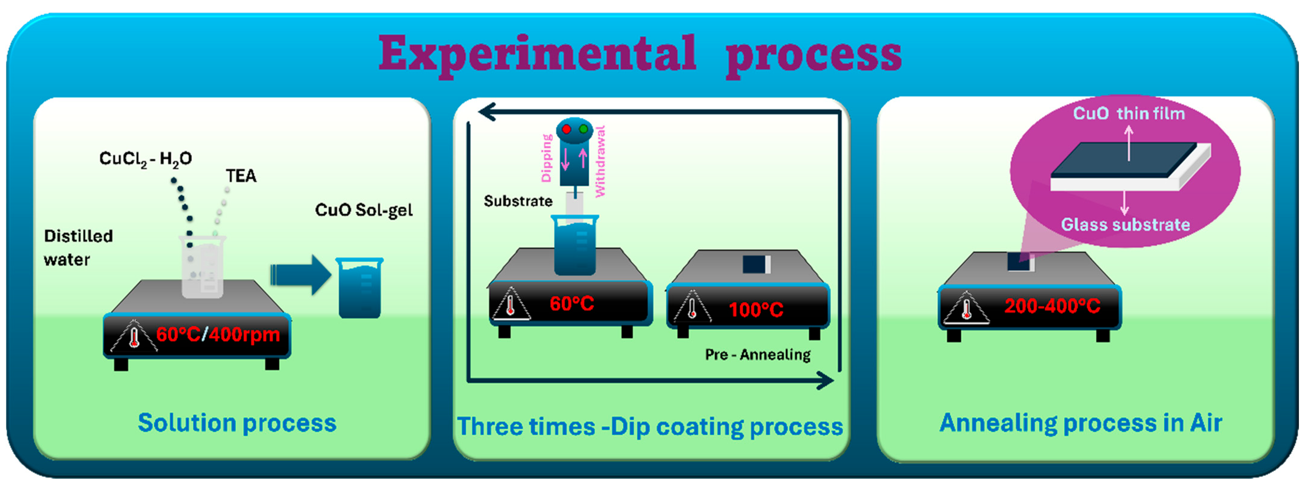
CuO thin films were deposited on glass substrates using the sol–gel dip-coating technique. The precursor solution was prepared from copper chloride dihydrate (CuCl2·2H2O), deionized water, and triethanolamine (TEA), which acts as a stabilizing and complexing agent. The dip-coating process consisted of three successive coating cycles performed at a controlled withdrawal speed of 40 mm·min−1. After each deposition, the films were pre-annealed at 100 °C for 60 s to remove residual solvents and promote film adhesion (Figure 1). Subsequently, the samples obtained were annealed at different temperatures (200, 300, and 400 °C) for 5 min to improve crystallinity and modify their physical properties.
The selection of three coating cycles and a short annealing time (5 min) was carefully optimized to achieve high-quality thin films with suitable structural and optical properties. The choice of three coating cycles was based on obtaining an optimal compromise between film thickness, uniformity, and adhesion. Preliminary experiments indicated that films prepared with fewer cycles were too thin and often discontinuous, whereas increasing the number of cycles resulted in excessively thick layers, leading to the development of internal stresses, microcracks, and deterioration of structural quality. This trend is consistent with previous studies [34], which report that the number of coating cycles plays a critical role in controlling film morphology, thickness, and mechanical stability, and that an intermediate number of cycles is generally required to ensure compact and homogeneous films. Regarding the annealing duration, the short annealing time of 5 min was selected to promote rapid crystallization while minimizing undesirable effects such as grain overgrowth, defect formation, or film degradation. Short thermal treatments are often sufficient to induce crystallinity in thin films, particularly when combined with optimized deposition conditions, as reported in the literature [35]. Prolonged annealing, on the other hand, may lead to structural coarsening and the formation of cracks due to thermal stress. Therefore, the adopted conditions (three coating cycles and 5 min annealing) were found to be optimal for achieving uniform, well-adhered, and structurally stable films with reproducible properties.
Prior to deposition, the glass substrates were carefully cleaned to ensure good film quality. The cleaning procedure involved immersion in diluted nitric acid, followed by rinsing in distilled water for 10 min and drying at 100 °C for 10 min.
The sol–gel dip-coating method adopted in this work offers several advantages, including simplicity, low cost, and suitability for large-area deposition. In addition, it is considered an environmentally friendly (eco-friendly) technique due to its low energy consumption, reduced chemical waste, and the possibility of using relatively non-toxic precursors. These features make it particularly attractive for scalable fabrication of metal oxide thin films. Commercial soda–lime glass substrates were selected due to their low cost, smooth surface, optical transparency, and widespread use in optoelectronic and photovoltaic applications. Their transparency is particularly advantageous for optical characterization of CuO thin films. Furthermore, these substrates provide adequate chemical stability and thermal resistance within moderate annealing temperature ranges. Typically, soda–lime glass can withstand temperatures below ~450–500 °C; exceeding this range may approach its strain and annealing points, leading to stress relaxation or deformation during thermal treatment, which must be avoided during film deposition and annealing processes.

2.2. Characterization of CuO Thin Layers

The structural properties of the deposited CuO thin films were studied between 2θ = 30 and 2θ = 60° by using X-ray diffraction (XRD) with CuKα radiation (λ = 1.54056 Å). Raman spectroscopy, ranging from 200 to 800 cm−1 using a wavelength laser (λ = 532 nm), was used to check the vibrational modes of CuO compounds. Optical properties were investigated using UV–visible spectrophotometry. The electrical properties were measured using the four-point probe technique. The structural properties of the deposited CuO thin films were analyzed using X-ray diffraction (XRD) with CuKα radiation (λ = 1.54056 Å), recorded over an appropriate 2θ range to identify the crystalline phase, preferred orientation, and degree of crystallinity. The texture coefficient (TC) was calculated to evaluate the preferential crystallographic orientation of the films. The optical properties were investigated using UV–visible spectrophotometry in the wavelength range of 300–800 nm. The transmittance (T%) and absorbance (Abs) spectra were recorded, and the absorption coefficient (α) was determined for further analysis. The optical band gap was estimated using the Tauc method by plotting (αhν)2 as a function of photon energy (hν).
The electrical properties of the films were measured at room temperature using the standard four-point probe technique, which allows accurate determination of sheet resistance while minimizing contact resistance effects. The electrical conductivity was then calculated by considering the measured sheet resistance and film thickness.
Film thickness was determined using the HebalOptics software, enabling correlation between structural, optical, and electrical properties. These complementary characterization techniques provide a comprehensive understanding of the relationships between processing conditions and the resulting properties of the CuO thin films.

3. Results and Discussion

3.1. Structural Properties

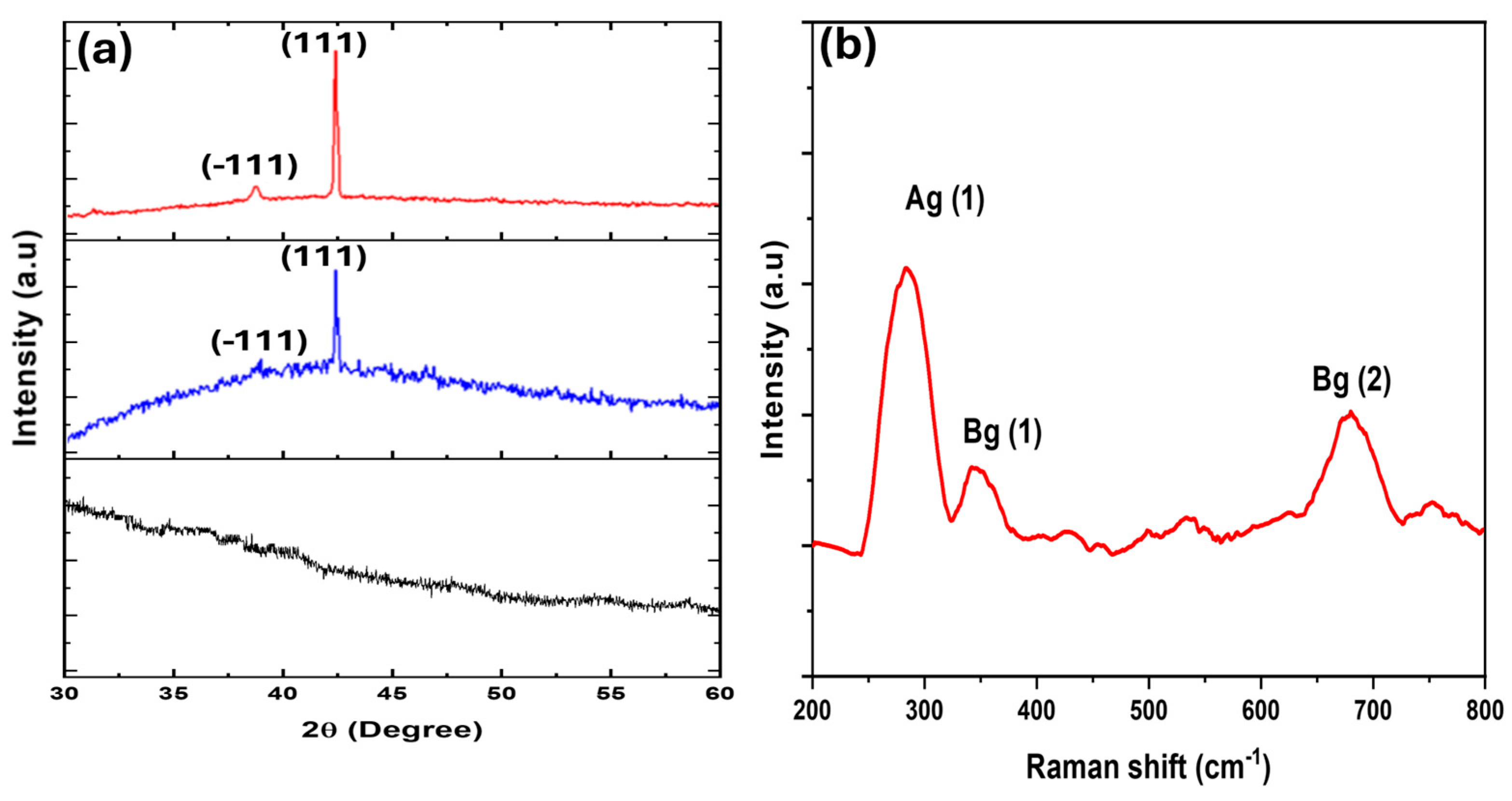
The X-ray diffraction (XRD) patterns of CuO thin films prepared by the dip-coating method and annealed at different temperatures are presented in Figure 2a. Two prominent diffraction peaks are observed at 2θ values of approximately 39° and 42.5°, which can be indexed to the (−111) and (111) crystallographic planes, respectively. According to the JCPDS card No. 80-1916, all detected peaks correspond to the tenorite CuO phase, confirming the formation of a monoclinic crystal structure. No additional peaks related to secondary phases or impurities are detected, indicating the successful synthesis of phase-pure CuO thin films. As illustrated in Figure 2a, the deposited films exhibit a pronounced preferential orientation along the (111) plane. This strong texturing suggests a high degree of crystallographic ordering. Notably, the structural quality obtained in this study for CuO films annealed in ambient air exceeds that reported in the literature for CuO films without preferential orientation prepared by DC planar magnetron sputtering followed by thermal oxidation under oxygen plasma [36]. To further confirm the phase formation, a representative Raman spectrum of CuO thin films annealed at 400 °C is shown in Figure 2b. As reported in the literature, the spectrum exhibits the characteristic Ag and Bg vibrational modes associated with monoclinic CuO [37,38]. These results are in excellent agreement with the XRD analysis and further validate the formation of phase-pure monoclinic CuO. The maximum annealing temperature was limited to 400 °C based on both material and substrate considerations. Since the films were deposited on soda–lime glass substrates, higher annealing temperatures may induce deformation, softening, or microcracking due to thermal expansion mismatch between the film and the substrate. XRD results demonstrate that the monoclinic CuO phase is fully developed with good crystallinity at 400 °C, indicating that higher temperatures are not required to achieve phase purity. Furthermore, previous studies have shown that annealing beyond this temperature mainly promotes excessive grain growth rather than significant structural improvement [39]. Such grain coarsening may reduce the effective surface area, which plays a crucial role in surface-controlled gas sensing mechanisms. In addition, as highlighted in the review by Steinhauer [40], the gas sensing response of CuO-based sensors typically occurs at operating temperatures significantly lower than the annealing temperature, and increasing the annealing temperature does not necessarily result in proportional enhancement of sensing performance. Therefore, an annealing temperature of 400 °C represents an optimal compromise, ensuring phase purity, improved crystallinity, and stable electrical properties, while avoiding substrate degradation and limiting excessive grain growth.
The structural analysis was further strengthened by extracting and reporting the full width at half maximum (FWHM) values of the diffraction peaks. An experimental uncertainty of ±0.01° was estimated based on three repeated XRD measurements performed under identical conditions, ensuring the reproducibility and reliability of the results. Although a full Rietveld refinement could provide more comprehensive quantitative structural information, the primary objective of this study is to investigate the evolution of crystallinity and preferential orientation as a function of annealing temperature. In this context, the analysis of diffraction peak positions and FWHM values is sufficient to confirm the formation of phase-pure monoclinic CuO and to assess the improvement in crystallinity. The preferential (111) orientation observed in the films can be explained by thermodynamic and kinetic factors governing thin film growth. During deposition, the system tends to minimize its total surface and interfacial energies, leading to the preferential development of specific crystallographic planes. In polycrystalline metal oxide films such as CuO, the (111) plane is often reported as a densely packed and energetically favorable orientation, particularly at elevated temperatures where enhanced atomic mobility facilitates crystallization and grain rearrangement [41]. Consequently, this orientation becomes dominant under optimized growth conditions. The presence of a strong (111) texture has important implications for the structural and functional properties of the films. It is generally associated with improved crystallinity, enhanced grain growth, and reduced defect density, all of which contribute to better electronic transport and improved optical performance [42,43]. Therefore, the evolution of the (111) preferential orientation with increasing temperature reflects an overall improvement in film quality.
Regarding the absence of XRD data at 200 °C, this is attributed to the very poor crystallinity of the films deposited at such a low temperature. Under these conditions, limited atomic mobility hinders proper crystal formation, resulting in extremely weak and broadened diffraction peaks that are insufficient for reliable phase identification or quantitative analysis. Consequently, structural parameter calculations could not be meaningfully performed for this sample. It is worth noting that the XRD pattern of the sample annealed at 200 °C is not presented, as no distinct diffraction peaks corresponding to crystalline CuO were detected. This suggests that the film remains amorphous or poorly crystallized at this temperature, thereby preventing the reliable extraction of structural parameters. The crystallite size (D) was estimated using the Scherrer equation, as reported in our recent work on 2D materials for energy storage applications [44]:
D = 0.9 λ β c o s θ
where λ is the Cu Kα wavelength (1.5406 Å), β is the full width at half maximum (FWHM) expressed in radians, and θ is the Bragg diffraction angle of the dominant (111) peak. The dislocation density ( δ ) and microstrain ( ε ) were estimated using Equations (2) and (3), respectively, and the texture coefficient Tc was recently used to estimate the microstructural parameters of metal oxide materials to detect some toxic gases [44]:
δ = 1 D 2
ε = β 4 t a n θ
Tc = I r ( h k l ) I 0 ( h k l ) 1 n 1 n I r ( h k l ) I 0 ( h k l )
The texture coefficient is calculated using the following formula [45], where Ir(hkl) represents the relative intensity of the (hkl) plane, while I0(hkl) is the standard intensity of the (hkl) plane extracted from (JCPDS card No. 80-1916). The texture coefficient (TC(hkl)) characterizes the texture of a specific plane, providing quantitative information about the preferential orientation of crystallites. A TC(hkl) value of one indicates randomly oriented crystallites in a thin layer, whereas higher values signify an abundance of grains in a particular (hkl) direction. The texture of a material significantly influences its structural and photoelectrical properties, as well as the performance and reliability of fabricated devices [46]. When TC is greater than one, it signifies a higher degree of orientation along the c-axis in our layers.
Table 1 summarizes the evolution of the microstructural parameters of CuO thin films annealed at 300 and 400 °C. A clear trend is observed, characterized by an increase in crystallite size (D), accompanied by a significant reduction in dislocation density (δ) and lattice strain (ε) with increasing annealing temperature. This behavior indicates a progressive improvement in the crystallinity and structural ordering of the CuO films upon thermal treatment. The crystallite size increases slightly from 17.79 nm to 19.34 nm for samples annealed at 300 and 400 °C, respectively. Although this difference remains moderate, it reflects the sensitivity of the microstructural properties to annealing conditions and demonstrates the ability to finely tune these parameters through controlled thermal processing. The reduction in lattice defects and internal strain further supports the enhancement of crystalline quality at higher annealing temperatures. The microstructural parameters were calculated using standard relations, as described in our previous work on 2D materials for energy storage applications [47].

3.2. Optical Properties

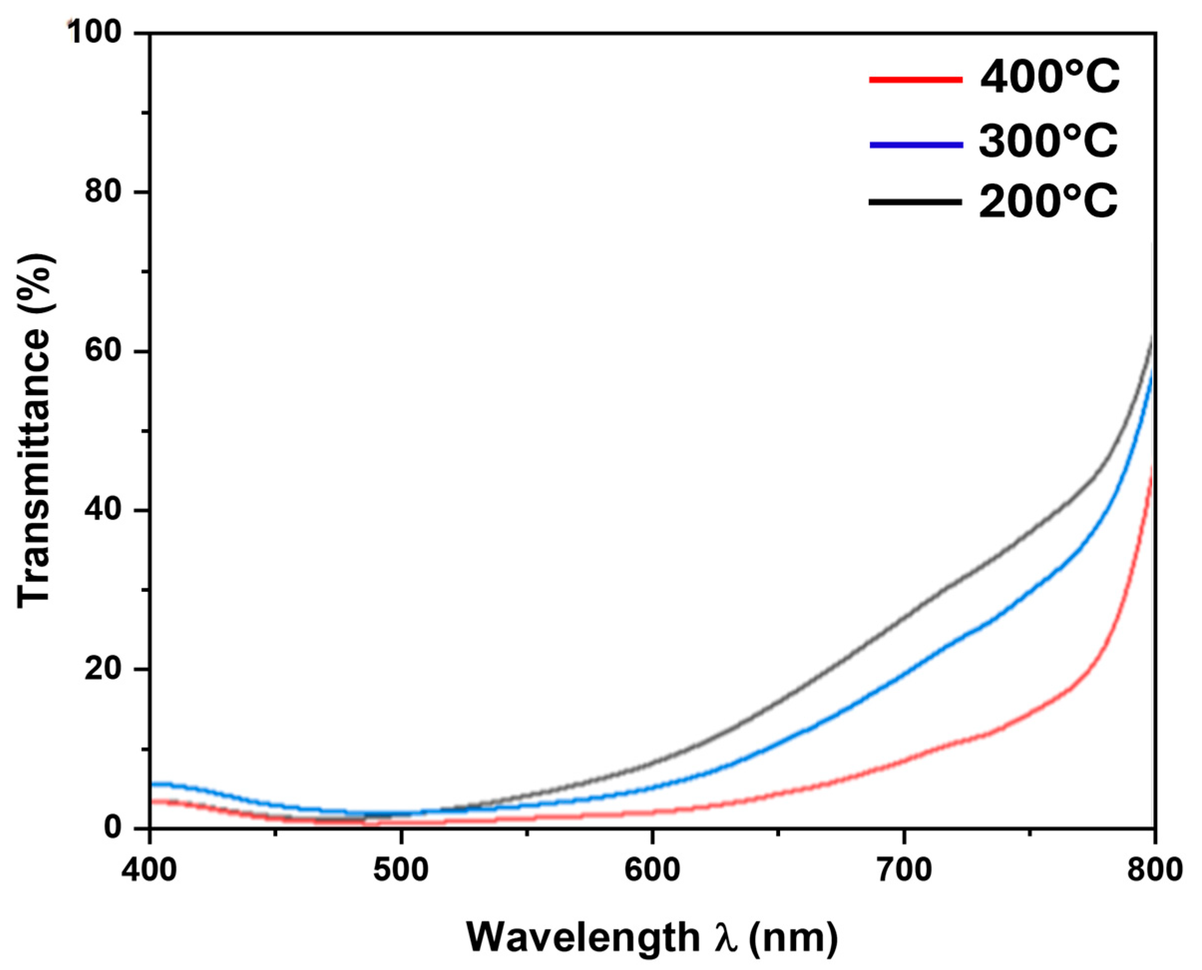
Figure 3 shows the optical transmittance spectra of CuO thin films annealed at 200, 300, and 400 °C. A clear decreasing trend in transmittance is observed with increasing annealing temperature. A more detailed analysis reveals that the transmittance (T%) strongly depends on both wavelength and thermal treatment. All films exhibit low transmittance values in the visible region, with a pronounced minimum around 500 nm, indicating enhanced optical absorption at this wavelength. Quantitatively, the transmittance decreases from approximately 3% for the film annealed at 200 °C to about 0.5% at 400 °C at 500 nm, the latter representing the lowest value recorded. This behavior can be attributed to improved crystallinity and film densification at higher annealing temperatures, which enhance light–matter interaction and reduce optical transmission. Similar trends have been reported for CuO thin films prepared by spray pyrolysis [48], confirming the consistency of the present results. In comparison, higher transmittance values of around 50% have been reported for CuO films deposited by DC sputtering [49], while commercial CuO samples typically exhibit transmittance values of approximately 10% [50]. These values remain significantly higher than those obtained in the present work, highlighting the strong absorber characteristics of the dip-coated CuO thin films.
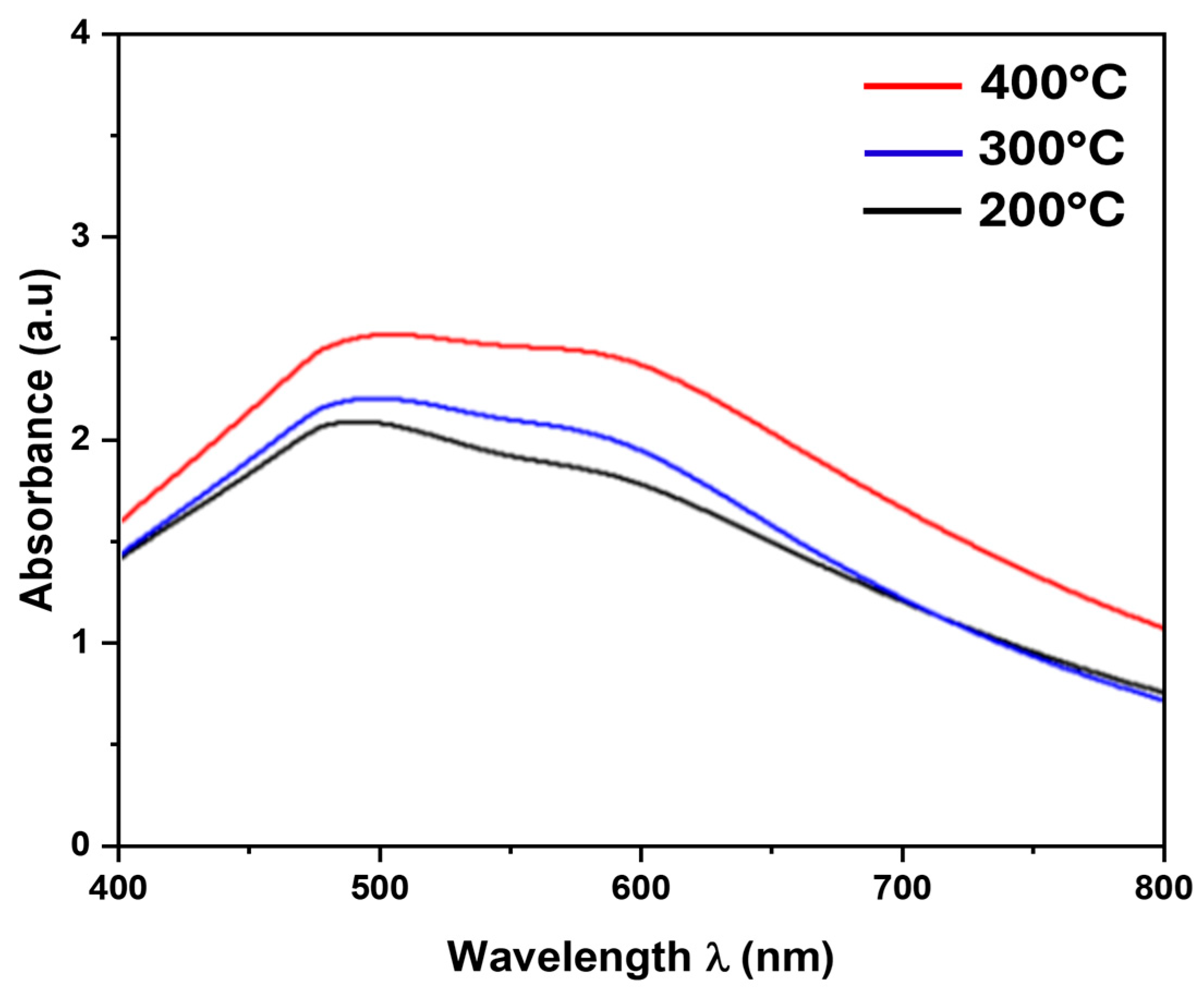
Figure 4 illustrates the variation in absorbance as a function of wavelength for CuO thin films annealed at different temperatures.
The absorbance spectra exhibit a behavior that is consistent with the transmittance results, showing a clear increase with increasing annealing temperature. A maximum absorbance is observed around 500 nm, corresponding to the low transmittance in this spectral region. Quantitatively, the absorbance increases from approximately 1.75 to 2.51 at 500 nm as the annealing temperature rises. The maximum value of approximately 2.51 is for the film annealed at 400 °C. This behavior can be primarily attributed to the improvement in crystallinity and structural quality at higher annealing temperatures, which enhances light absorption within the material. Furthermore, this trend highlights the ability to effectively tune the optical absorption properties of CuO thin films through controlled annealing. It is worth emphasizing that the optical performance achieved using the cost-effective sol–gel dip-coating method is comparable to that of CuO films fabricated by more advanced techniques such as RF magnetron sputtering and reactive plasma deposition using a high target utilization sputtering (HiTUS) system [51]. Lower absorbance values have been reported for CuO thin films prepared by alternative deposition techniques. For instance, spin-coated CuO films exhibit relatively low absorbance values below 0.4 [52], whereas CuO films fabricated via chemical vapor deposition (CVD), despite the higher processing cost, show absorbance values of approximately 2.5 [53]. These comparisons highlight the significant variation in optical absorption behavior depending on the fabrication method and resulting film microstructure. The combination of low transmittance and high absorbance observed for all samples suggests that CuO thin films are promising absorber materials for photovoltaic applications. This advantage is particularly significant when compared to more complex quaternary compounds such as CCTS and CIGaS, which rely on relatively expensive and less abundant elements such as cobalt (Co), indium (In), and gallium (Ga), and may involve more demanding fabrication processes, including adhesion challenges that require additional energy input [54,55].
In addition to optical absorption, the transmittance of thin films is strongly influenced by surface roughness due to light scattering effects. Although direct measurements of surface roughness (via AFM) were not available in the present study, further insight was gained through structural analysis based on X-ray diffraction data. Specifically, the texture coefficient (TC) was calculated to assess the degree of preferred crystallographic orientation and crystallinity of the films deposited at different temperatures. The TC is widely recognized as an indicator of film texture and is indirectly related to surface morphology and roughness [56]. The results show that the film deposited at 400 °C exhibits the highest TC value, indicating a pronounced preferential orientation and improved crystalline quality. Such enhanced structural ordering is expected to reduce defect density and minimize scattering centers, thereby improving the optical transparency of the films. Therefore, the variation in transmittance observed in Figure 3 can be primarily attributed to the improvement in crystallinity and texture surface with increasing deposition temperature, rather than being solely governed by surface roughness effects. These findings emphasize the close relationship between structural properties and optical behavior in the studied films.
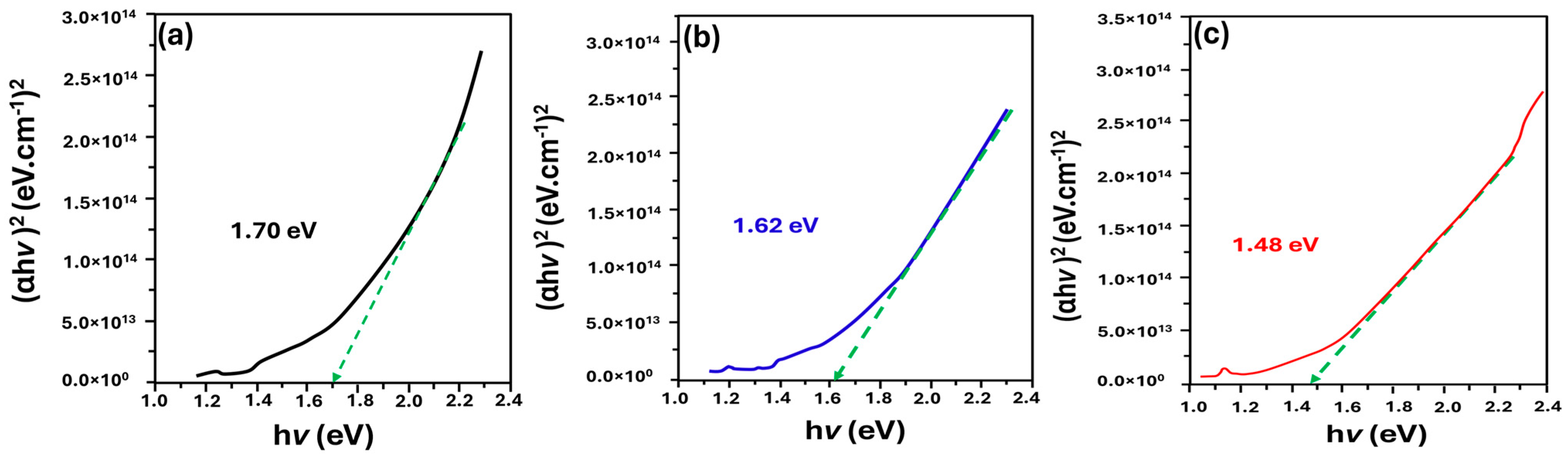
Figure 5a–c presents the plots of α h ν ) 2 as a function of photon energy h ν for CuO thin films deposited on glass substrates via the dip-coating technique and annealed at different temperatures.
The optical band gap of the films was determined using the Tauc relation, expressed as:
α h ν ) n = A ( h ν E g
where α is the absorption coefficient, h ν is the incident photon energy, A is a constant, and n depends on the nature of the electronic transition. In the present study, a value of n = 2 was adopted, corresponding to an allowed direct transition. Although bulk CuO is generally reported to exhibit an indirect band gap, several studies on CuO thin films have demonstrated that a direct transition model can provide a good approximation, particularly in systems exhibiting structural disorder, reduced dimensionality, or mixed-phase characteristics [57]. This behavior is often attributed to modifications in the electronic structure induced by film morphology and growth conditions. The band gap values were therefore extracted by extrapolating the linear region of the α h ν 2 versus h ν plot to α h ν ) 2 0 . The obtained values are in good agreement with those reported in the literature for CuO thin films, supporting the validity of the adopted approach. Nevertheless, it is important to note that the coexistence of indirect transition characteristics cannot be completely excluded, and this aspect has been considered in the discussion to provide a comprehensive interpretation of the optical behavior.
The direct optical band gap Eg values were determined by linear extrapolation of the α h ν ) 2 curves using the Tauc relation, as commonly reported in the literature [58]. The estimated band gap values show a gradual decrease with increasing annealing temperature, decreasing from 1.70 eV at 200 °C to 1.62 eV at 300 °C, and further to 1.48 eV at 400 °C. This reduction in band gap is consistent with the enhanced optical absorption observed in Figure 4 and can be attributed to the improvement in crystallinity of the CuO thin films. Higher crystallinity reduces structural defects and grain boundaries, which typically act as scattering centers and non-radiative recombination sites that hinder effective light absorption. As the annealing temperature increases, the XRD peaks become sharper and more intense, indicating improved structural ordering, which correlates well with the observed enhancement in optical absorption. Although direct quantification of defect density was not performed, the narrowing and increased intensity of the diffraction peaks provide indirect evidence of improved crystallinity, in agreement with previous studies [59,60].
The observed decrease in optical band gap with increasing annealing temperature can also be explained by this structural improvement. At higher temperatures, grain growth and the reduction in grain boundary density lead to decreased structural disorder, which is often associated with band tailing effects and artificially widened band gaps. Consequently, the effective optical band gap slightly decreases. Similar trends have been reported for CuO and other metal oxide thin films, where improved crystallinity results in a modest reduction in band gap values [59,60]. The obtained band gap values further confirm the semiconducting nature of CuO and highlight its suitability for gas sensing applications based on semiconductor mechanisms [61]. Moreover, the values reported here are consistent with those obtained for CuO thin films prepared by sol–gel and dip-coating methods in previous studies [62]. It is also noteworthy that these results are comparable to those achieved using other oxide materials, such as Co3O4 thin films fabricated by cost-effective techniques with enhanced photo-response [63], as well as to more complex and expensive absorber materials, including CIS, CIGS, CdTe, AgZTS, and CMnTS, which are widely used in photovoltaic applications [64,65,66,67,68]. Overall, the combination of low optical band gap, high absorbance, and low transmittance supports the potential of the prepared CuO thin films as efficient absorber layers for solar cell applications.

3.3. Electrical Properties

The electrical characterization of CuO thin layers, prepared through the dip-coating method, was conducted using a four-wire apparatus. Similar to Co3O4 and Mn3O4, CuO exhibited P-type conductivity. Table 2 presents the observed variations in electrical resistivity and conductivity of the CuO thin layers. The values for these electrical parameters were calculated twice using Equations (5) and (6) [69].
ρ = R × d
σ = 1 ρ
where (R) is the measured resistance of CuO thin layers given by a four-wire apparatus, (ρ) is the electrical resistivity, and (σ) is the electrical conductivity.
The film thickness d , required for resistivity calculations, was determined using the HebalOptics software (HO) based on optical transmittance modeling, following the approach reported in [70]. The obtained results indicate a gradual decrease in thickness from approximately 2.0 µm and 1.8 µm for films annealed at 200 °C and 300 °C, respectively, to about 1.0 µm for the film annealed at 400 °C. This reduction is attributed to film densification during thermal treatment, which promotes the removal of residual solvents and enhances structural compactness. The estimated uncertainty in thickness measurements is ±0.02 µm. In electrical characterization, resistivity ρ is defined as the intrinsic property of a material that quantifies its opposition to the flow of electric current under an applied electric field [71]. Conversely, electrical conductivity σ describes the ability of a material to facilitate the transport of charge carriers, thereby enabling current flow [72].
Electrical measurements revealed that all CuO thin films exhibited resistivity values within the range of 10–100 Ω·cm, consistent with previously reported data in [73].
The electrical properties of the films exhibit a clear dependence on the annealing temperature, as evidenced by the progressive decrease in sheet resistance from 20.49 ± 0.3 kΩ/sq at 200 °C to 16.27 ± 0.2 kΩ/sq at 400 °C, accompanied by an increase in electrical conductivity from 48 S·m−1 to 61 S·m−1. This improvement in conductivity can be attributed to several concurrent mechanisms. First, increasing the annealing temperature enhances crystallinity, as confirmed by XRD analysis, leading to a reduction in structural defects that typically act as charge carrier trapping centers. Second, grain growth and improved grain boundary connectivity reduce carrier scattering, thereby facilitating more efficient charge transport. Additionally, the observed decrease in film thickness (from 2 µm to 1 µm) suggests film densification, which contributes to better compactness and reduced porosity, further improving electrical pathways. These effects collectively lead to enhanced carrier mobility and, consequently, higher conductivity at elevated annealing temperatures. Similar trends have been reported in the literature [74,75], where annealing-induced structural improvement and densification play a key role in optimizing the electrical performance of metal oxide thin films. Electrical conductivity is a critical parameter for gas sensor performance, as higher conductivity typically enhances sensor response [76]. Therefore, the observed improvements in the electrical properties of CuO thin films, particularly the increase in conductivity, demonstrate the significant influence of annealing temperature on the functional quality of the films. These results highlight the potential of the prepared CuO layers as effective sensitive materials for gas sensor applications.
* Novel highly oriented CuO thin layers for future resistive gas sensing
Resistive-type CuO gas sensors require materials with specific characteristics, including stable semiconducting behavior, reproducible and measurable electrical resistance, high crystallinity, and a microstructure conducive to surface adsorption and gas–surface interactions. In this context, the dip-coated CuO thin films prepared in this study exhibit stable semiconducting behavior with well-defined and reproducible resistance values, demonstrating their suitability for resistance-based sensing devices. The progressive improvement in crystallinity with increasing annealing temperature enhances charge transport properties, which is essential for achieving reliable and stable sensor responses. XRD analysis reveals a strong preferential orientation along the (111) plane of monoclinic CuO. This crystallographic alignment is associated with relatively high surface atomic density and enhanced surface reactivity, which can promote oxygen adsorption and facilitate interactions with target gases. Given that the sensing mechanism in metal oxide semiconductors is primarily governed by surface reactions involving adsorbed oxygen species and analyte gases, such preferential orientation is expected to positively influence sensing performance. Although dip-coating has been widely employed for CuO thin film fabrication, previous studies have generally reported films with lower crystallinity and less pronounced preferential orientation [77,78]. The novelty of the present work lies in the fabrication of highly oriented CuO thin films (~1 µm thick) via a low-cost sol–gel dip-coating method, yielding microstructures approaching monocrystalline-like domains. Compared with more complex and expensive deposition techniques such as reactive sputtering [79], chemical vapor deposition (CVD) [80], and atomic layer deposition (ALD) [81], which require sophisticated equipment, controlled atmospheres, and longer processing times, the sol–gel dip-coating approach adopted here is simple, cost-effective, rapid, and scalable for large-area deposition. Beyond structural optimization, this study establishes clear correlations between annealing temperature, crystallinity enhancement, optical band gap evolution, and electrical resistivity. Analysis of the optical band gap provides insight into the electronic structure, defect states, and charge carrier transitions of the films, which directly influence electrical conductivity and resistance modulation during gas sensing. The combined structural, optical, and electrical investigations therefore offer a comprehensive understanding of the structure–property relationships in dip-coated CuO thin films, providing new insights not fully addressed in previous studies and highlighting their potential as effective active layers for future resistive gas sensor applications.

4. Conclusions

In summary, CuO thin films were successfully prepared via the sol–gel method and deposited on standard glass substrates using the dip-coating technique. The influence of annealing temperature on the structural, optical, and electrical properties of the films was systematically investigated. X-ray diffraction analysis confirmed the formation of a pure tenorite phase with a monoclinic structure, exhibiting a strong preferential orientation along the (111) plane. Microstructural analysis indicated well-defined nanoscale crystallites with sizes ranging from 17.79 to 19.34 nm. UV–visible spectroscopy revealed the superior optical characteristics of the CuO films, showing high absorbance and low transmittance compared to other optical materials. The semiconducting properties of the films were strongly influenced by annealing, with a notable decrease in the optical band gap from 1.70 eV to 1.48 eV. Electrical measurements demonstrated that annealing also improved the conductivity of the films, increasing from 4.8 to 6.1 S·m−1. These results indicate that annealing temperature is a critical parameter for tuning the properties of CuO thin films. Among the studied conditions, annealing at 400 °C provided the optimal combination of structural, optical, and electrical properties, making the resulting CuO films highly suitable as active layers for resistive gas sensors based on metal oxide semiconductors.

Author Contributions

Conceptualization, Y.D.; methodology, Y.D.; software, Y.D.; validation, Y.D.; formal analysis, Y.D.; investigation, Y.D.; resources, Y.D.; data curation, Y.D.; writing—original draft preparation, Y.D.; writing—review and editing, Y.D.; visualization, Y.D.; supervision, B.H., M.S. P.T. and A.B.; project administration, Y.D. and B.H.; funding acquisition, Y.D. and A.B. All authors have read and agreed to the published version of the manuscript.

Funding

This research received no external funding.

Data Availability Statement

The data will be made available on request.

Conflicts of Interest

The authors declare no conflict of interest.

References

  1. Guo, Y.; Zhu, L.; Wang, X.; Qiu, X.; Qian, W.; Wang, L. Assessing environmental impact of NOX and SO2 emissions in textiles production with chemical footprint. Sci. Total Environ. 2022, 831, 154961. [Google Scholar] [CrossRef]
  2. Xu, Y.; Zhang, W.; Huo, T.; Streets, D.G.; Wang, C. Investigating the spatio-temporal influences of urbanization and other so-cioeconomic factors on city-level industrial NOx emissions: A case study in China. Environ. Impact Assess. Rev. 2023, 99, 106998. [Google Scholar] [CrossRef]
  3. Chan, Y.H.; Lock, S.S.M.; Wong, M.K.; Yiin, C.L.; Loy, A.C.M.; Cheah, K.W.; Chai, S.Y.W.; Li, C.; How, B.S.; Chin, B.L.F.; et al. A state-of-the-art review on capture and separation of hazardous hydrogen sulfide (H2S): Recent advances, challenges and outlook. Environ. Pollut. 2022, 314, 120219. [Google Scholar] [CrossRef]
  4. Sobieraj, K.; Dabrowska, S.S.; Luo, G.; Koziel, J.A.; Bialowiek, A. Carbon Monoxide Fate in the Environment as an Inspiration For Biorefinery Industry: A Review. Front. Environ. Sci. 2022, 10, 822463. [Google Scholar] [CrossRef]
  5. Vithanage, M.; Bandara, P.C.; Novo, L.A.B.; Kumar, A.; Ambade, B.; Naveendrakumar, G.; Ranagalage, M.; Arachchi, D.N.M. Deposition of trace metals associated with atmospheric particulate matter: Environmental fate and health risk assessment. Chemosphere 2022, 303, 135051. [Google Scholar] [CrossRef]
  6. Xu, Y.; Ou, Q.; Jiao, M.; Liu, G.; Van der Hoek, J.P. Identification and Quantification of Nanoplastics in Surface Water and Groundwater by Pyrolysis Gas Chromatography-Mass Spectrometry. Environ. Sci. Technol. 2022, 56, 4988–4997. [Google Scholar] [CrossRef]
  7. Visconti, G.; Boccard, J.; Feinberg, M.; Rudaz, S. From fundamentals in calibration to modern methodologies: A tutorial for small molecules quantification in liquid chromatography–mass spectrometry bioanalysis. Anal. Chim. Acta 2023, 1240, 340711. [Google Scholar] [CrossRef] [PubMed]
  8. Goel, N.; Kunal, K.; Kushwaha, A.; Kumar, M. Metal oxide semiconductors for gas sensing. Eng. Rep. 2022, 5, e12604. [Google Scholar] [CrossRef]
  9. Zhang, Y.; Jiang, Y.; Yuan, Z.; Liu, B.; Zhao, Q.; Huang, Q.; Li, Z.; Zeng, W.; Duan, Z.; Tai, H. Synergistic Effect of Electron Scattering and Space Charge Transfer Enabled Unprecedented Room Temperature NO2 Sensing Response of SnO2. Small 2023, 19, 2303631. [Google Scholar] [CrossRef]
  10. Wei, W.; Zhang, H.; Tao, T.; Xia, X.; Bao, Y.; Lourenco, M.; Homewood, K.; Huang, Z.; Gao, Y. A CuO/TiO2Heterojunction Based CO Sensor with High Response and Selectivity. Energy Environ. Mater. 2022, 6, e12570. [Google Scholar] [CrossRef]
  11. Kim, K.; Choi, P.G.; Itoh, T.; Masuda, Y. Effect of Coordinatively Unsaturated Sites in MOF-Derived Highly Porous CuO for Catalyst-Free ppb-Level Gas Sensors. Adv. Mater. Interfaces 2021, 8, 2100283. [Google Scholar] [CrossRef]
  12. Kumarage, G.W.C.; Zappa, D.; Mihalcea, C.G.; Maraloiu, V.-A.; Stefan, M.; Comini, E. Revolutionizing n-type Co3O4 Nanowire for Hydrogen Gas Sensing. Adv. Energy Sustain. Res. 2023, 4, 2300067. [Google Scholar] [CrossRef]
  13. Umar, A.; Ibrahim, A.A.; Nakate, U.T.; Albargi, H.; Alsaiari, M.A.; Ahmed, F.; Alharthi, F.A.; Alghamdi, A.A.; Al-Zaqri, N. Fabrication and characterization of CuO nanoplates based sensor device for ethanol gas sensing application. Chem. Phys. Lett. 2021, 763, 138204. [Google Scholar] [CrossRef]
  14. Sultana, J.; Paul, S.; Karmakar, A.; Yi, R.; Dalapati, G.K.; Chattopadhyay, S. Chemical bath deposited (CBD) CuO thin films on n-silicon substrate for electronic and optical applications: Impact of growth time. Appl. Surf. Sci. 2017, 418, 380–387. [Google Scholar] [CrossRef]
  15. Absike, H.; Essalhi, Z.; Labrim, H.; Hartiti, B.; Baaalla, N.; Tahri, M.; Jaber, B.; Ez-zahraouy, H. Synthesis of CuO thin films based on Taguchi design for solar absorber. Opt. Mater. 2021, 118, 111224. [Google Scholar] [CrossRef]
  16. Khot, S.; Phalake, S.; Mahadik, S.; Baragale, M.; Jagadale, S.; Burungale, V.; Navale, Y.; Patil, V.; Patil, V.; Patil, P.; et al. Synthesis of CuO thin film sensors by spray pyrolysis method for NO2 gas detection. Mater. Today Proc. 2021, 43, 2694–2697. [Google Scholar] [CrossRef]
  17. Menazea, A.A.; Mostafa, A.M. Ag doped CuO thin film prepared via pulsed laser deposition for 4-nitrophenol degradation. J. Environ. Chem. Eng. 2020, 8, 104104. [Google Scholar] [CrossRef]
  18. Doubi, Y.; Hartiti, B.; Batan, A.; El-Gheryby, Y.; Thevenin, P. Sustainable electrochemical growth of highly oriented (-111) CuO absorber layers for optoelectronic applications. Mater. Today Commun. 2026, 50, 114477. [Google Scholar] [CrossRef]
  19. Dolai, S.; Dey, R.; Das, S.; Hussain, S.; Bhar, R.; Pal, A.K. Cupric oxide (CuO) thin films prepared by reactive d.c. magnetron sputtering technique for photovoltaic application. J. Alloys Compd. 2017, 724, 456–464. [Google Scholar] [CrossRef]
  20. Tripathi, T.S.; Terasaki, I.; Karppinen, M. Anomalous thickness- dependent optical energy gap of ALD- grown ultra-thin CuO films. J. Phys. Condens. Matter 2016, 28, 475801. [Google Scholar] [CrossRef]
  21. Wang, Y.; Wang, Y.; Xiang, Z.; Li, X. A novel “Snowflake”—rGO-CuO for ultrasonic degradation of rhodamine and methyl orange. Nano Mater. Sci. 2024, 6, 365–373. [Google Scholar] [CrossRef]
  22. Xie, X.; Ke, J.; Liu, F.; Qiu, L.; Zhang, Z.; Huang, S.; Chen, X. P-type CuO for chemiresistive gas sensing: From nanostructures to sensing mechanisms. Microchem. J. 2025, 218, 115642. [Google Scholar] [CrossRef]
  23. Govind, A.; Bharathi, P.; Harish, S.; Krishna Mohan, M.; Archana, J.; Navaneethan, M. Interface engineering of a highly sensitive porous CuO modified rGO layers for room temperature NO2 gas sensor. Appl. Surf. Sci. 2024, 657, 159604. [Google Scholar] [CrossRef]
  24. Rydosz, A. The Use of Copper Oxide Thin Films in Gas-Sensing Applications. Coatings 2018, 8, 425. [Google Scholar] [CrossRef]
  25. Rakshit, B.S.; Mondal, S.; Jana, P.C.; Datta, R. CuO nanoparticles: Structural, optical and electronic properties with gas sensing performance for efficient detection of NO2 gas. J. Mater. Sci. Mater. Electron. 2025, 36, 1260. [Google Scholar] [CrossRef]
  26. Madhukeswara, A.R.S.; Shashidhar, R.; Raghu, A.; Prakasha, G.S. Influence of air annealing on the microstructural, mor-phological, compositional, optical and electrical properties of spray deposited CuO thin films and their utility as MOM gas sensors. Emergent Mater. 2024, 7, 2891–2906. [Google Scholar] [CrossRef]
  27. Claros, M.; Gracia, I.; Figueras, E.; Vallejos, S. Hydrothermal Synthesis and Annealing Effect on the Properties of Gas-Sensitive Copper Oxide Nanowires. Chemosensors 2022, 10, 353. [Google Scholar] [CrossRef]
  28. Chang, H.; Feng, S.; Qiu, X.; Meng, H.; Guo, G.; He, X.; He, Q.; Yang, X.; Ma, W.; Kan, R.; et al. Implementation of the toroidal absorption cell with multi-layer patterns by a single ring surface. Opt. Lett. 2020, 45, 5897–5900. [Google Scholar] [CrossRef] [PubMed]
  29. Feng, R.; Yu, Y.; Wu, L.; Wang, J.; Tan, Q.; Burokur, S.N. Full-space programmable metasurface for Bessel beam tailoring. Opt. Lett. 2025, 50, 5161–5164. [Google Scholar] [CrossRef] [PubMed]
  30. He, Y.; Zhang, B.; Zhou, S.; Wei, Y.; Li, B.; Wang, H. Stepwise Removal Mechanism of Impurity Using Multi-Flux During Blister Copper Pyrometallurgical Refining. Metall. Mater. Trans. B 2026, 57, 134–148. [Google Scholar] [CrossRef]
  31. Wang, G.; Yang, Y.; Zhou, S.; Li, B.; Wei, Y.; Wang, H. Data Analysis and Prediction Model for Copper Matte Smelting Process. Metall. Mater. Trans. B 2024, 55, 2552–2567. [Google Scholar] [CrossRef]
  32. Wang, X.; Chen, J.; He, X.; Lin, M.; Hou, Z.; Yu, C.; Lu, H.; Xiong, K. The impact of Ni and Zn doping on the stability, electrical and thermal conductivity of intermetallic compounds between Sn solder and Cu substrate. Vacuum 2025, 240, 114527. [Google Scholar] [CrossRef]
  33. Hao, Y.; Su, Z.; Li, W.; Fang, X.; Wang, D.; Fang, D.; Li, J.; Xu, S.; Du, P. Characteristics of carrier localization and their effects on minority carrier lifetime in InAs/In0.5Ga0.5As0.5Sb0.5 type II superlattices. Appl. Phys. Lett. 2025, 127, 082105. [Google Scholar] [CrossRef]
  34. Martínez-Saucedo, G.; Castanedo-Pérez, R.; Torres-Delgado, G.; Mendoza-Galván, A.; Zelaya Ángel, O. Cuprous oxide thin films obtained by dip-coating method using rapid thermal annealing treatments. Mater. Sci. Semicond. Process. 2017, 68, 133–139. [Google Scholar] [CrossRef]
  35. Srivastava, A.; Singh, R.; Tripathi, S. Design and analysis of visible photonics resonators coated with CuO thin film. Nanotechnology 2020, 31, 155201. [Google Scholar] [CrossRef] [PubMed]
  36. Mohammed, E.A. Effect of Annealing on Sensing Properties of ZnO: CuO Nanocomposite Thin Films by the Sol-gel Method. Neuroquantology 2022, 20, 32–38. [Google Scholar] [CrossRef]
  37. Charrada, G.; Ajili, M.; Jebbari, N.; Hajji, M.; Bernardini, S.; Aguir, K.; Kamoun, N.T. Investigation on thermal annealing effect on the physical properties of CuO-SnO2:F sprayed thin films for NO2 gas sensor and solar cell simulation. Mater. Lett. 2024, 367, 136666. [Google Scholar] [CrossRef]
  38. Hojabri, A.; Hajakbari, F.; Soltanpoor, N.; Hedayati, M.S. Annealing temperature effect on the properties of untreated and treated copper films with oxygen plasma. J. Theor. Appl. Phys. 2014, 8, 132. [Google Scholar] [CrossRef]
  39. Lei, O.; Huang, L.; Yin, J.; Davaasuren, B.; Yuan, Y.; Dong, X.; Wu, Z.-P.; Wang, X.; Yao, K.X.; Lu, X.; et al. Structural evolution and strain generation of derived- Cu catalysts during CO2 electrreduction. Nat. Commun. 2022, 13, 4857. [Google Scholar] [CrossRef]
  40. Mo, X.; Hu, J.; Shen, H.; Shui, L.; Shu, D.; He, J.; He, G.; Wang, Y.; Li, W.; He, Q. Surface modification of micro-sized CuO by in-situ growing heterojunctions CuO/Cu2O and CuO/Cu2O/Cu: Effect on surface charges and photogenerated carrier lifetime. Appl. Phys. A 2018, 124, 719. [Google Scholar] [CrossRef]
  41. Itoh, T.; Maki, K. Preferentially oriented thin-film growth of CuO(1 1 1) and Cu2O(0 0 1) on MgO(0 0 1) substrate by reactive dc-magnetron sputtering. Vacuum 2007, 81, 904–910. [Google Scholar] [CrossRef]
  42. Hu, J.; Li, D.; Lu, J.G.; Wu, R. Effects on Electronic Properties of Molecule Adsorption on CuO Surfaces and Nanowires. J. Phys. Chem. C 2010, 114, 17120–17126. [Google Scholar] [CrossRef]
  43. Navale, Y.H.; Navale, S.T.; Stadler, F.J.; Ramgir, N.S.; Debnath, A.K.; Gadkari, S.C.; Gupta, S.K.; Aswal, D.K.; Patil, V.B. Thermally evaporated copper oxide films: A view of annealing effect on physical and gas sensing properties. Ceram. Int. 2017, 43, 7057–7064. [Google Scholar] [CrossRef]
  44. Doubi, Y.; Hartiti, B.; Batan, A.; Siadat, M.; Labrim, H.; Tahri, M.; Kotbi, A.; Thevenin, P.; Jouiad, M. Sensors and Actuators B. Chemical 2025, 440, 137878. [Google Scholar]
  45. El khalidi, Z.; Hartiti, B.; Fadili, S.; Thevenin, P. Nickel oxide optimization using Taguchi design for hydrogen detection. Int. J. Hydrog. Energy 2018, 43, 12574–12583. [Google Scholar] [CrossRef]
  46. Asl, H.Z.; Rozati, S.M. Influence of texture coefficient on the electrical properties of spray-deposited fluorine-doped tin oxide thin film. J. Mater. Sci. Mater. Electron. 2021, 32, 1668–1676. [Google Scholar] [CrossRef]
  47. Steinhauer, S. Gas sensors based on copper oxide nanomaterials: A review. Chemosensors 2021, 9, 51. [Google Scholar] [CrossRef]
  48. Moumen, A.; Hartiti, B.; Comini, E.; El khalidi, Z.; Munasinghe Arachchige, H.M.M.; Fadili, S.; Thevenin, P. Preparation and characterization of nanostructured CuO thin films using spray pyrolysis technique. Superlattices Microstruct. 2019, 127, 2–10. [Google Scholar] [CrossRef]
  49. Alfaro Cruz, M.R.; Sanchez-Martinez, D.; Torres-Martínez, L.M. CuO thin films deposited by DC sputtering and their photo-catalytic performance under simulated sunlight. Mater. Res. Bull. 2020, 122, 110678. [Google Scholar] [CrossRef]
  50. Mohammedi, A.; Charik, H.; Oudjertli, S.; Ibrir, M.; Hocini, A.; Khezami, L.; Guesmi, A.; Fellah, M. Enhancing efficiency of low-power all-optical switching through nonlinear optical properties of CuO thin films. J. Indian Chem. Soc. 2026, 103, 102583. [Google Scholar] [CrossRef]
  51. Al-Ghamdi, A.A.; Khedr, M.H.; Ansari, M.S.; Hasan, P.M.Z.; Abdel-wahab, M.S.; Farghali, A.A. RF sputtered CuO thin films: Structural, optical and photo-catalytic behavior. Phys. E Low-Dimens. Syst. Nanostructures 2016, 81, 83–90. [Google Scholar] [CrossRef]
  52. Dahrul, M.; Alatas, H. Preparation and Optical Properties Study of CuO thin Film as Applied Solar Cell on LAPAN-IPB Satellite. Procedia Environ. Sci. 2016, 33, 661–667. [Google Scholar] [CrossRef]
  53. Narin, P.; Kutlu-Narin, E.; Ardali, S.; Sarikavak-Lisesivdin, B.; Tiras, E.; Lisesivdin, S.B. Temperature controlled phase transition and characterization of Cu2O and CuO thin films grown at different growth temperatures via mist CVD. Appl. Phys. A 2026, 132, 377. [Google Scholar] [CrossRef]
  54. Hammami, H.; Marzougui, M.; Oueslati, H.; Ben Rabeh, M.; Kanzari, M. Synthesis, Growth and Characterization of Cu2CoSnS4 thin films via thermal evaporation method. Optik 2021, 227, 166054. [Google Scholar] [CrossRef]
  55. Bouich, A.; Ullah, S.; Ullah, H.; Mari, B.; Hartiti, B.; Touhami, M.E.; Santos, D.M.F. Deposit on different back contacts: To high-quality CuInGaS2 thin films for photovoltaic application. J. Mater. Sci. Mater. Electron. 2019, 30, 20832–20839. [Google Scholar] [CrossRef]
  56. Kumar, M.; Kumar, A.; Abhyankar, A.C. Influence of Texture Coefficient on Surface Morphology and Sensing Properties of W-Doped Nanocrystalline Tin Oxide Thin Films. ACS Appl. Mater. Interfaces 2015, 7, 3571–3580. [Google Scholar] [CrossRef]
  57. Said, M.I.; Othman, A.A.; Abdelhakeem, E.M. Structural, optical and photocatalytic properties of mesoporous CuO nano-particles with tunable size and different morphologies. RCS Adv. 2021, 11, 37801–37813. [Google Scholar]
  58. Doubi, Y.; Hartiti, B.; Siadat, M.; Labrim, H.; Fadili, S.; Tahri, M.; Stitou, M.; Thevenin, P.; Losson, E. Experimental Investigation of Pure Spinel Mn3O4 Properties Synthesized through Chemical Spray Pyrolysis for Future Gas Sensor Application. Eur. J. Inorg. Chem. 2023, 26, e202300047. [Google Scholar] [CrossRef]
  59. Yevdokymenko, V.Y.; Dobrozhan, O.; Pshenychnyi, R.; Opanasyuk, A.; Gnatenko, Y.; Bukivskii, A.; Bukivskij, P.; Gamernyk, R.; Klymov, O.; Muñoz-Sanjosé, V.; et al. The effect of annealing treatment on the structural and optical properties of nanostructured CuxO films obtained by 3D printing. Mater. Sci. Semicond. Process. 2023, 161, 107472. [Google Scholar] [CrossRef]
  60. Habibi, M.H.; Karimi, B. Effect of the annealing temperature on crystalline phase of copper oxide nanoparticle by copper acetate precursor and sol–gel method. J. Therm. Anal. Calorim. 2014, 115, 419–423. [Google Scholar] [CrossRef]
  61. Tran, T.H.; Nguyen, M.H.; Nguyen, T.H.T.; Dao, V.P.T.; Nguyen, P.M.; Nguyen, V.T.; Pham, N.H.; Le, V.V.; Sai, C.D.; Nguyen, Q.H.; et al. Effect of annealing temperature on morphology and structure of CuO nanowires grown by thermal oxidation method. J. Cryst. Growth 2019, 505, 33–37. [Google Scholar] [CrossRef]
  62. Kariper, I.A. Structural, optical and porosity properties of CdI2 thin film. J. Mater. Res. Technol. 2016, 5, 77–83. [Google Scholar] [CrossRef]
  63. Moumen, A.; Hartiti, B.; Thevenin, P.; Siadat, M. Synthesis and characterization of CuO thin films grown by chemical spray pyrolysis. Opt. Quantum Electron. 2017, 49, 1–12. [Google Scholar] [CrossRef]
  64. Doubi, Y.; Hartiti, B.; Labrim, H.; Tahri, M.; Laazizi, A.; Thevenin, P. Elaoration of spinel Co3O4 via cost effective chemical spray pyrolysis for enhanced photo-response. Mater. Today Commun. 2024, 40, 110207. [Google Scholar] [CrossRef]
  65. Mahmoud, F.; Eliwa, A.; Ahmed, N.; Magdy, W. Sprayed single phase CuIn0.6Ga0.4S thin films for solar cell applications; Sol-vent-dependent growth. J. Optoelectron. Adv. Mater. 2016, 18, 268–274. [Google Scholar]
  66. Daza, L.G.; Canché-Caballero, V.; Chan y Díaz, E.; Castro-Rodríguez, R.; Iribarren, A. Tuning optical properties of CdTe films with nanocolumnar morphology grown using OAD for improving light absorption in thin-film solar cells. Superlattices Microstruct. 2017, 111, 1126–1136. [Google Scholar] [CrossRef]
  67. Abdullah, S.M.; Bakr, N.A.; Salaman, S.A. Structural, optical, and electrical properties of Ag2ZnSnS4 sprayed thin films by chemical pyrolysis method. Chalcogenide Lett. 2021, 18, 65–73. [Google Scholar] [CrossRef]
  68. Salh, A.J.; Bakr, N.A. Structural, optical, and electrical properties of chemically sprayed Cu2MnSnS4 thin films. Chalcogenide Lett. 2022, 19, 483–492. [Google Scholar] [CrossRef]
  69. Doubi, Y.; Hartiti, B.; Siadat, M.; Labrim, H.; Fadili, S.; Stitou, M.; Tahri, M.; Belfhaili, A.; Thevenin, P.; Losson, E. Optimization with Taguchi Approach to Prepare Pure TiO2 Thin Films for Future Gas Sensor Application. J. Electron. Mater. 2022, 51, 3671–3683. [Google Scholar] [CrossRef]
  70. Roguai, S.; Djelloul, A.; Nouveau, C.; Souier, T.; Dakhel, A.A.; Bououdina, M. Structure, microstructure and determination of optical constants from transmittance data of co-doped Zn0. 90Co0. 05M0. 05O (MAl, Cu, Cd, Na) films. J. Alloys Compd. 2014, 599, 150–158. [Google Scholar] [CrossRef]
  71. Dawood, Y.Z. The Influence of Substrate Temperature on CdS Thin Films Properties Prepared by Pulse Laser Deposition on Glass Substrates. Energy Procedia 2017, 119, 536. [Google Scholar] [CrossRef]
  72. Singh, A.K.; Chowdhury, N.K.; Roy, S.C.; Bhowmik, B. Review of Thin Film Transistor Gas Sensors: Comparison with Resistive and Capacitive Sensors. J. Electron. Mater. 2022, 51, 1974–2003. [Google Scholar] [CrossRef]
  73. Djebian, R.; Boudjema, B.; Kabir, A.; Sedrati, C. Physical characterization of CuO thin films obtained by thermal oxidation of vacuum evaporated Cu. Solid State Sci. 2022, 101, 106147. [Google Scholar] [CrossRef]
  74. Jamal, M.S.; Shahahmadi, S.A.; Chelvanathan, P.; Alharbi, H.F.; Karim, M.R.; Dar, M.A.; Luqman, M.; Alharthi, N.H.; AlHarthi, Y.S.; Aminuzzaman, M.; et al. Effects of growth temperature on the photovoltaic properties of RF sputtered undoped NiO thin films. Results Phys. 2019, 14, 102360. [Google Scholar] [CrossRef]
  75. Zhang, C.; Gunes, O.; Wen, S.J.; Yang, Q.; Kasap, S. Effect of Substrate Temperature on the Structural, Optical and Electrical Properties of DC Magnetron Sputtered VO2 Thin Films. Materials 2022, 15, 7849. [Google Scholar] [CrossRef] [PubMed]
  76. Bolar, S.; Shit, S.; Kumar, J.S.; Murmu, N.C.; Ganesh, R.S.; Inokawa, H.; Kuila, T. Optimization of active surface area of flower like MoS2 using V-doping towards enhanced hydrogen evolution reaction in acidic and basic medium. Appl. Catal. B Environ. 2019, 254, 432–442. [Google Scholar] [CrossRef]
  77. Amri, A.; Hasan, K.; Taha, H.; Rahman, M.M.; Herman, S.; Andrizal; Awaltanova, E.; Wantono, I.; Kabir, H.; Yin, C.-Y.; et al. Surface structural features and optical analysis of nanostruc-tured Cu-oxide thin film coatings coated via the sol-gel dip coating method. Ceram. Int. 2019, 45, 1288–1294. [Google Scholar] [CrossRef]
  78. Mustafa, H.A.; Hamad, S.M.; Jameel, D.A. Effects of dip-coating cycles on green synthesis of CuO thin film, structural, optical, and electrical properties. J. Mater. Sci. Mater. Electron. 2026, 37, 148. [Google Scholar] [CrossRef]
  79. Zeng, X.; Zhukova, M.; Faniel, S.; Proost, J.; Flandre, D. Structural and Opto-electronic characterization of CuO thin films pre-pared by DC reactive magnetron sputtering. J. Mater. Sci. Mater. Electron. 2020, 31, 4563–4573. [Google Scholar] [CrossRef]
  80. Eisermann, S.; Kronenberger, A.; Laufer, A.; Bieber, J.; Haas, G.; Lautenschläger, S.; Homm, G.; Klar, P.J.; Meyer, B.K. Copper oxide thin films by chemical vapor deposition: Synthesis, characterization and electrical properties. Phys. Status Solidi (A) 2011, 209, 531–536. [Google Scholar] [CrossRef]
  81. He, D.; Du, L.; Wang, K.; Ding, Y. Efficient Process of ALD CuO and Its Application in Photocatalytic H2 Evolution. Russ. J. Inorg. Chem. 2021, 66, 1986–1994. [Google Scholar] [CrossRef]
Figure 1. Schematic diagram showing the dip-coating method adopted for CuO thin-layer fabrication.
Coatings 16 00551 g001
Figure 2. Structural characterization of CuO thin films: (a) X-ray diffraction patterns of CuO layers annealed at 200, 300 and 400 °C; (b) typical Raman spectrum of the CuO thin film annealed at 400 °C.
Coatings 16 00551 g002
Figure 3. Transmittance spectra of CuO thin layers annealed at 300 and 400 °C.
Coatings 16 00551 g003
Figure 4. Absorbance spectra of CuO thin layers annealed at 200, 300 and 400 °C.
Coatings 16 00551 g004
Figure 5. Variation of (ahv)2 versus hv of CuO thin layers annealed at three temperatures: (a) 200, (b) 300 and (c) 400 °C.
Coatings 16 00551 g005
Table 1. Micro-structural parameters of CuO thin layers annealed at 300 and 400 °C.
Annealing
Temperature (°C)
FWHM (Degree)Crystallite Size
D (nm)
Dislocation Density
δ × 10−2 (nm−2)
Micro-strain
ε × 10−3
Texture Coefficient Tc (111)
200 - - - - 0
3000.49 ± 0.0517.793.155.611.42
4000.45 ± 0.0419.340.265.162.29
Table 2. Electrical parameters of CuO thin layers annealed at 200, 300 and 400 °C.
Annealing
Temperature (°C)
Thickness (µm)Resistance (kΩ/sq)Conductivity
(S.m−1)
2002 ± 0.0220.49 ± 0.348
3001.8 ± 0.0218.39 ± 0.3254
4001 ± 0.0216.27 ± 0.261
Disclaimer/Publisher’s Note: The statements, opinions and data contained in all publications are solely those of the individual author(s) and contributor(s) and not of MDPI and/or the editor(s). MDPI and/or the editor(s) disclaim responsibility for any injury to people or property resulting from any ideas, methods, instructions or products referred to in the content.