Article

Investigation of the Microstructure and Properties of Cage-Shaped Hollow Cathode Bias Voltage Modulated Si-Doped DLC Thick Film

1
School of Materials Science and Engineering, Jiamusi University, Jiamusi 154007, China
2
School of Chemical Equipment, Shenyang University of Technology, Liaoyang 111003, China
*
Authors to whom correspondence should be addressed.
These authors contributed equally to this work.
Coatings 2025, 15(8), 930; https://doi.org/10.3390/coatings15080930
Submission received: 23 July 2025 / Revised: 4 August 2025 / Accepted: 5 August 2025 / Published: 8 August 2025
(This article belongs to the Section Thin Films)

Abstract

To mitigate the high residual stress inherent in single-layer diamond-like carbon (DLC) films, we fabricate alternating soft/hard multilayer DLC thick films using a cage-type hollow cathode plasma-enhanced chemical vapor deposition (PECVD) system. The microstructure, mechanical properties, and corrosion resistance of these films were systematically investigated. Periodic film structures were characterized via scanning electron microscopy (SEM), Raman spectroscopy, atomic force microscopy (AFM), and X-Ray photoelectron spectroscopy (XPS). Adhesion and hardness were evaluated using a scratch tester and a nanoindentation tester, respectively, while corrosion resistance was assessed by dynamic potential polarization tests in a 3.5 wt% NaCl solution. Findings indicate that as the modulation period of the Si-DLC films increases, a greater proportion of high-energy carbon particles penetrate the non-biased layer under workpiece bias, ultimately disrupting the layered structure in the 90-layer film. This results in densification, reflected in three key improvements: (1) an increase in sp3-bonded carbon content and enhanced smoothness, (2) enhanced adhesion (from 34 N to 46 N) and nanohardness (from 4.94 GPa to 8.41 GPa), and (3) a tenfold reduction in corrosion current density (icorr) compared to single-layer Si-DLC films.

1. Introduction

With the increasing focus on the development of strategic marine resources, numerous unprecedented challenges and issues have emerged. Notably, critical mechanical components such as pipes, hydraulic systems, and thrust bearings exhibit distinct failure mechanisms when exposed to seawater, including wear and corrosion, which significantly impact the safety, reliability, and service life of marine equipment [1,2,3]. Consequently, there is an urgent need to develop self-lubricating materials suitable for direct application in marine environments. One of the most effective strategies involves the use of thick and robust films characterized by high wear and corrosion resistance [4,5,6]. Diamond-like carbon (DLC) films have garnered considerable attention due to their low friction coefficient, high hardness, and excellent wear and corrosion resistance [7,8,9]. However, the high internal stress generated during the growth of DLC films poses a challenge, particularly for films exceeding a thickness of 10 μm [10]. The continuous accumulation of stress during the deposition process ultimately leads to the delamination and failure of the DLC film.
According to relevant reports, composite processing increases the hardness of the substrate and reduces substrate deformation under external loads, thereby improving its load-bearing capacity [11,12,13]. The mesh plasma immersion ion deposition (MPIID) technology employs a cage-type hollow cathode discharge to prepare DLC thin films. This process is highly controllable, with a high deposition rate and capability to deposit complex shapes in large volumes [14]. Furthermore, the design of the bias multi-layer film not only alleviates internal stress but also densifies the DLC film layer, thereby enhancing adhesion strength. While numerous studies have explored the integration of composite treatment with thin DLC films [15,16,17], there is a paucity of research concerning thick DLC films [18].
In our previous research, we explored the integration of laser cladding technology with DLC film composite treatment, capitalizing on its advantages such as energy efficiency, environmental sustainability, minimal heat input, and strong metallurgical bonding with the substrate. This integration was found to enhance the adhesion strength and corrosion resistance of DLC films. The present study aims to examine the impact of varying bias modulation periods on the adhesion and corrosion resistance of DLC films under high deposition rate conditions. In this investigation, we initially employed a laser to create a cladding layer (LC) on the substrate. Subsequently, we utilized cage-type hollow cathode discharge technology to deposit a silicon-doped DLC (Si-DLC) modulated film onto the LC. A comprehensive analysis of the adhesion mechanism of the Si-DLC modulated film was conducted.

2. Materials and Methods

The bias-modulated Si-DLC multilayer deposition system was described in detail in Reference [14]. The substrate utilized is normalized 45# steel with dimensions of 50 mm (L) × 50 mm (W) × 10 mm (H). Prior to deposition of the Si-DLC modulation film, we first prepared an approximately 1 mm thick Fe–Cr alloy cladding layer on the 45# steel surface using an HWL-6000 laser cladding system. The composition of the Fe–Cr alloy powder is provided in Table 1. The laser cladding parameters were as follows: laser power = 1500 W, powder feed rate = 33 g/min, and scan speed = 3 mm/s. After cladding, the surface was sequentially ground using silicon carbide sandpaper (500 to 2000 grit) and polished with a 2.5 μm diamond suspension. The samples were then cut into 15 mm (L) × 15 mm (W) × 11 mm (H) blocks using wire electrical discharge machine (EDM). Prior to deposition, these blocks, along with Si wafers used for evaluating the Si-DLC film thickness, were ultrasonically cleaned in anhydrous ethanol for 30 min at room temperature.
The sample was placed in a vacuum chamber filled with high-purity argon as the working gas, along with reaction gases including C2H2 and tetramethylsilane (TMS). Under a base pressure of 5 × 10⁻³ Pa, an argon plasma discharge was initiated using a cage grid pulse voltage of −1400 V and a workpiece bias voltage of −200 V at a gas pressure of 3.5 Pa. The workpiece was pre-cleaned via argon sputtering for 30 min to remove surface contaminants. Subsequently, a Si transition layer was deposited by introducing TMS, followed by C2H2 to initiate the growth of the DLC layer. To modulate the sublayer thickness (ranging from micrometers to nanometers), the bias voltage was alternated between 0 V and −200 V during deposition, producing three sets of Si-DLC multilayer films. A monolithic Si-DLC film (fabricated without bias voltage modulation) served as the control group.
Figure 1 schematically illustrates the layered film design, while Table 2 summarizes the corresponding deposition parameters. The samples were labeled as follows:
L0: single-layer Si-DLC (control);
L18, L30, L90: multilayer films with modulation periods of 18, 30, and 90, respectively.
The surface and cross-sectional morphology of the Si-DLC film, along with its composition, were characterized utilizing a JEOL JSM-780F (JEOL, Tokyo, Japan) field emission scanning electron microscope (SEM) equipped with an energy dispersive spectrometer (EDS). The film’s microstructure was examined via Raman spectroscopy (Horiba LabRam HR Evolution spectrometer, Horiba, Kyoto, Japan), with a 532 nm laser excitation. X-Ray photoelectron spectrometer (XPS, ESCALAB 250, Waltham, MA, USA) was used to determine the elemental composition and chemical bonding states, while atomic force microscopy (AFM, Bruker Dimension Icon, Bruker, Billerica, MA, USA) was employed to assess surface morphology and roughness.
Adhesion strength between the film and the substrate was quantified using an automatic scratch tester (model WS-2005, Zhongke Kaihua Technology Development Co., Ltd., Lanzhou, China) under a load of 50 N, with a loading speed of 50 N/min and a scratch length of 5 mm. For each sample, five scratches were made from the center to the edge. The hardness and elastic modulus of the film were measured using a Bruker TI 980 nanoindenter (Bruker, Minneapolis, MN, USA). To minimize substrate effects, the indentation depth was limited to 1/10 of the film thickness when determining the nanoindentation hardness and Young’s modulus. All tests were conducted at room temperature (25 °C) on the central region of the sample, with five measurements averaged to ensure reproducibility. Additionally, friction and wear resistance of the Si-DLC films were examined using a ball-on-disk tribometer (SFT-2M, Institute of Chemical Physics, Chinese Academy of Sciences, Lanzhou, China) with a 4 mm ZrO2, ceramic ball as the counterface, subjected to a load of 500 g, a rotational speed of 200 rpm, a wear track radius of 2 mm, and a testing duration of 10 min. For electrochemical characterization, Tafel polarization and electrochemical impedance spectroscopy (EIS) were conducted in 3.5 wt% NaCl solution using a standard three-electrode system. Prior to testing, the sample was immersed for 30 min to stabilize the open-circuit potential (OCP). EIS test covered a frequency range of 10−2 to 105 Hz, with 10 mV AC amplitude, while polarization scans were set at a rate of 10 mV·s−1.

3. Results

3.1. SEM Image of the Films

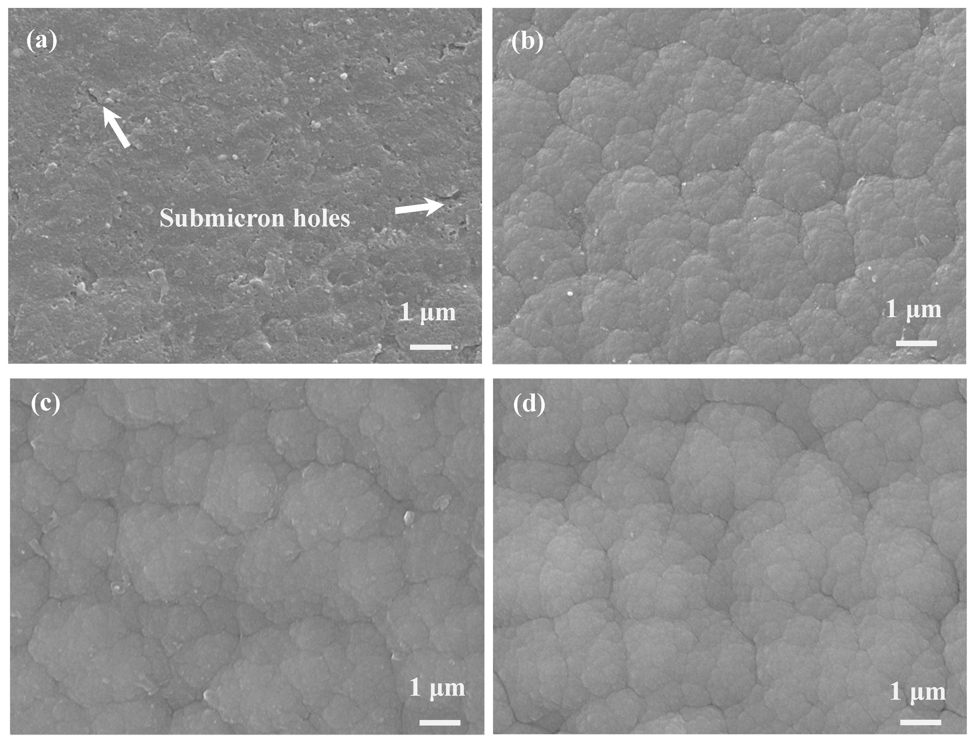
Figure 2 illustrates the surface morphology of Si-DLC single-layer and bias-modulated multilayer films. In Figure 2a–d, submicron holes are evident on the L0 sample’s surface (marked by arrows). While the L18, L30, and L90 Si-DLC modulated films display cellular protrusions, with increased modulation periods leading to smoother surfaces.
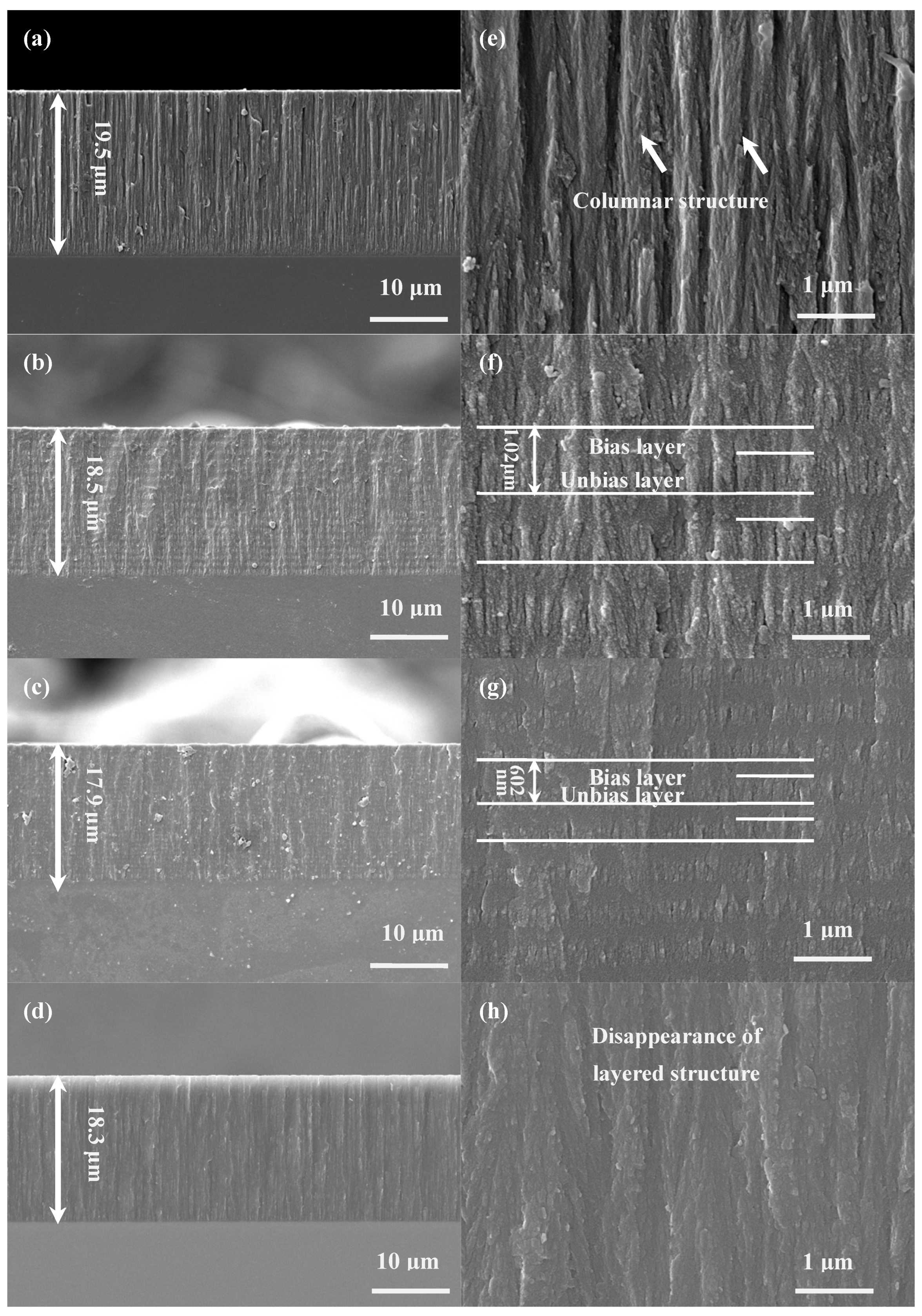
Figure 3 illustrates the cross-sectional morphology of the films. As observed in Figure 3a–d, the L0 film exhibits a columnar crystal structure. In contrast, the Si-DLC films with 18 and 30 modulation periods display a layered structure, whereas the film with a 90 modulation period transitions to a denser, glassy structure. The thickness of the Si-DLC monolayer film is approximately 19.5 µm, which is greater than that of the modulated films. This difference is primarily attributed to ion bombardment, which reduces deposition rates and enhances film densification [19].

3.2. Surface Roughness

Figure 4 presents the 2D AFM image of the Si-DLC modulation film surface, with a scanning area of 5 μm × 5 μm. As depicted in Figure 4a, the surface of the L0 film, which is not subjected to additional bias, exhibits considerable roughness. The surface morphology of the L0 film is characterized by hemispherical particles with top diameters ranging from 200 to 500 nm and a roughness average (Ra) value of 34.7 nm. Figure 4b–d illustrate that, under a 0 V/−200 V bias, the particles on the Si-DLC film surface become more densely packed, and the number of smaller hemispherical particles increases. The Ra values for the surface roughness of samples L18, L30, and L90 demonstrate a decreasing trend, with values of 31.0 nm, 28.5 nm, and 27.7 nm, respectively; however, these values remain higher than those reported for Si-DLC films in other studies [20]. The roughness of Si-DLC films is primarily influenced by the substrate surface roughness. As the thickness of Si-DLC films increases, their roughness values also tend to increase [21]. The application of a bias to the Si-DLC film enhances the lateral movement of surface-deposited particles, thereby increasing the smoothness of the film layer and reducing its roughness [22].

3.3. Raman Spectroscopy

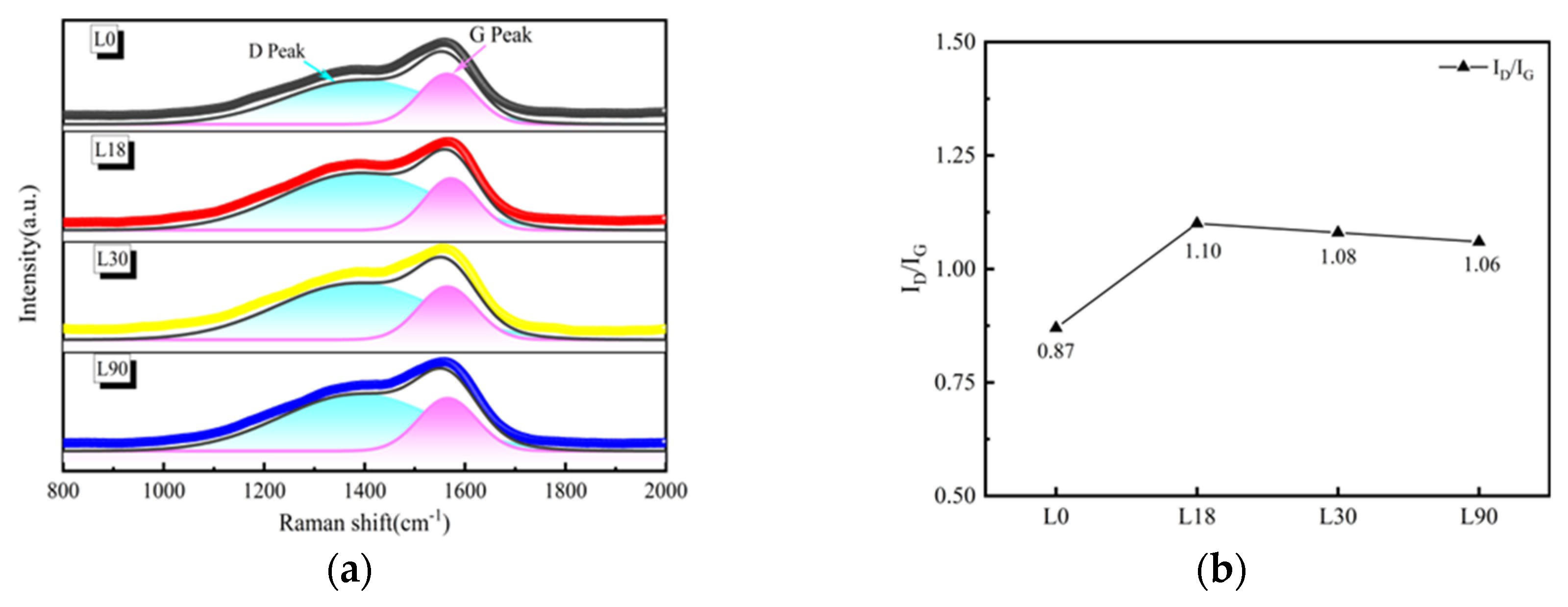
Figure 5 presents the Raman spectrum of the Si-DLC film. As illustrated in Figure 5a, all spectral lines fall within the range of 800 cm−1 to 2000 cm−1. The characteristic peak of asymmetric, hydrogen-containing amorphous DLC films is observed at approximately 1500 cm−1. Following the subtraction of the polymer baseline (PL), a double Gaussian fit was applied to analyze the structure of the Si-DLC film [23]. Two distinct peaks are identified at 1380 cm−1 and 1560 cm−1, corresponding to the D peak and G peak, respectively.
As depicted in Figure 5b, an increase in the number of Si-DLC modulated layers initially results in an increase in the ID/IG ratio, followed by a gradual decrease. This analysis suggests that, in comparison to single-layer Si-DLC films, the multi-layer modulated sublayer structure introduces more defects at the cross-section, leading to higher ID/IG values. As the modulation period increases, the unbiased layer within a single period becomes thinner, enhancing the uniformity of high-energy carbon particle bombardment and reducing the interface defect density, which in turn causes a gradual decrease in ID/IG values. For a detailed analysis, please refer to Section 3.5.

3.4. XPS

The ID/IG ratio obtained from Raman spectroscopy offers only qualitative insights into the structural characteristics of Si-DLC films, rendering it inadequate for determining the sp3/sp2 ratio within these films. Consequently, to further elucidate the structural composition of the Si-DLC film, X-Ray photoelectron spectroscopy (XPS) was employed to analyze the chemical bonding structure of each constituent element. As depicted in Figure 6a, the XPS survey spectrum of the Si-DLC film predominantly reveals the presence of C, Si, and O. The weak oxygen peak may be attributed to the TMS precursor serving as the silicon source or to water vapor adsorbed on the vacuum chamber walls, as suggested by previous studies [24].
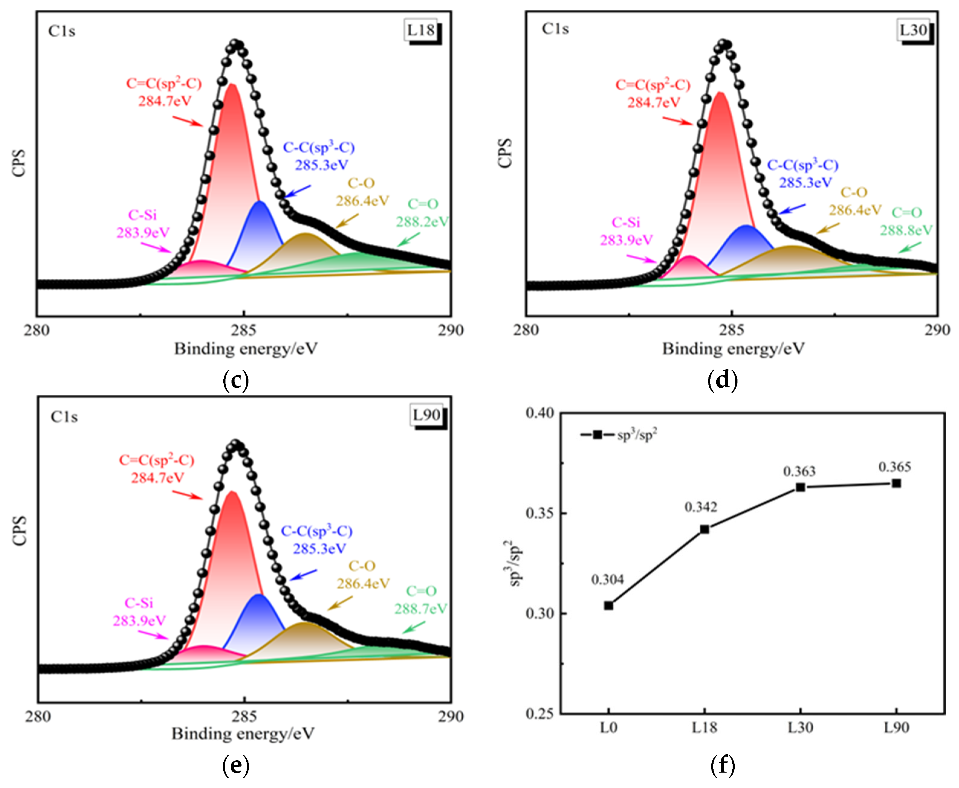
Figure 6b–d presents the Gaussian-Lorentzian fitting of the C1s fine spectrum following the deconvolution of the Si-DLC film, as referenced in [25]. The C1s spectrum is centered at 284.8 eV, with distinct peaks observed at 284.7 eV, 285.3 eV, 283.9 eV, 286.4 eV, and approximately 288.2 eV, which correspond to C=C (sp2) bonds, C–C (sp3) bonds, C–Si bonds, C–O bonds, and C=O bonds, respectively. The proportion of sp3 bonds within Si-DLC films plays a crucial role in determining the film’s performance. The ratio of sp3 to sp2 bonds is quantified by the relative areas of the sp3 and sp2 hybridization bond peaks, as noted in [26]. As illustrated in Figure 6f, the sp3/sp2 ratio in the modulated Si-DLC film exceeds that of the single-layer Si-DLC film, which is 0.304, suggesting a higher concentration of sp3 bonds in the modulated film. Furthermore, as the number of layers in the modulated film increases, the sp3/sp2 ratio rises to 0.342, 0.363, and 0.365, respectively.

3.5. Structural Evolution Mechanism

According to the subplantation model theory [27], the conversion of sp2 bonds to sp3 bonds in DLC films occurs as follows: the initially deposited carbon film predominantly comprises sp2-bonded graphite structures. Subsequently, high-energy carbon atoms collide with the deposited carbon film, resulting in the transformation of sp2 bonds to sp3 bonds within its sublayer, which extends from tens to hundreds of nanometers. When the impact energy of an individual carbon particle is approximately 100 eV, the rate of transformation is notably elevated. Figure 7 illustrates a schematic representation of the carbon particle bombardment region during the deposition process of Si-DLC modulation films. In scenarios where the modulation period is minimal, the thickness of the unbiased Si-DLC layer within a single period is considerable, leading to bombardment primarily affecting its surface layer, as depicted in Figure 7. Conversely, as the modulation period increases, the thickness of the unbiased Si-DLC layer progressively diminishes, approaching the penetration depth of carbon particles, thereby facilitating uniform reinforcement throughout the entire thickness for each modulation period. The findings indicate that with an increase in the number of modulation layers, (i) the surface roughness of the Si-DLC film progressively diminishes, resulting in enhanced smoothness. (ii) At a modulation period of 90, the layered structure of the Si-DLC film is entirely eliminated, accompanied by an increase in film density. Concurrently, (iii) there is a further augmentation in the proportion of sp3 bonds within the Si-DLC film.

3.6. Mechanical Properties

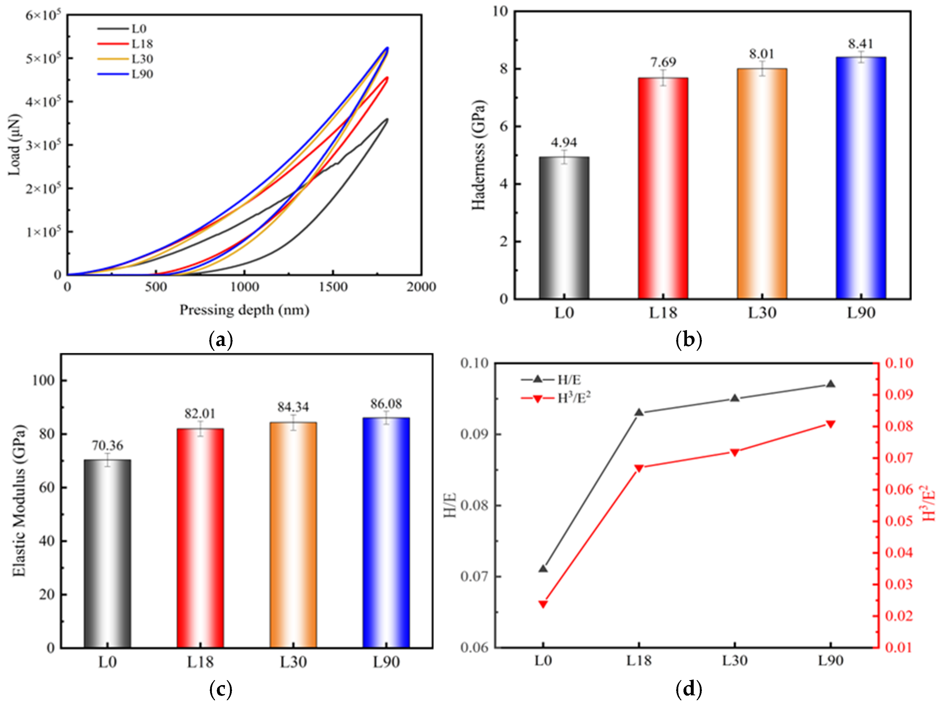
Figure 8 illustrates the nano-hardness and elastic modulus of the Si-DLC film. The maximum indentation depth, measured at 1.8 μm, constitutes approximately one-tenth of the film’s total thickness. The hardness of the single-layer Si-DLC film is recorded at 4.94 Gpa, whereas the hardness values for the L18, L30, and L90 Si-DLC modulated films are 7.69 Gpa, 8.01 Gpa, and 8.41 Gpa, respectively. In the L90 sample, ion bombardment of the biased layer results in the unbiased layer reaching the ion penetration depth, facilitating the conversion of sp2 to sp3 bonds, as corroborated by Raman and XPS analyses. The content of sp3 bonds exhibits a positive correlation with both hardness and elastic modulus, with the L90 modulated films displaying the highest sp3 bond content. Furthermore, the increase in the number of modulation layer interfaces, the densification of the microstructure, and the reduction in columnar structures collectively enhance the hardness and elastic modulus of Si-DLC films [28]. The H/E and H3/E2 ratios of Si-DLC modulated films significantly exceed those of Si-DLC monolayer films, with the L90 Si-DLC modulated films exhibiting the highest values, as depicted in Figure 8d.
Figure 9 illustrates the scratch morphology of the Si-DLC film. Here, we denote Lc1 as the initial fracture point (corresponding to the first crack appearance), Lc2 as the flake fracture point (corresponding to the first large-area spalling), and Lc3 as the final failure point (corresponding to the complete detachment of the film from the substrate). As depicted in Figure 9, the Lc3 value for the single-layer Si-DLC film is 34 N. In contrast, the Si-DLC modulated film exhibits superior adhesion compared to the single-layer Si-DLC film. With an increase in the number of modulation layers, the Lc3 values for L18, L30, and L90 are observed to be 35 N, 44 N, and 46 N, respectively. The analysis indicates that this enhanced adhesion can be attributed to several factors: (i) the high hardness and elastic modulus of the Si-DLC modulated film, which augment its load-bearing capacity; (ii) the alternating soft and hard multilayer structure of the Si-DLC modulated film, which facilitates crack deflection at the layer interfaces, thereby dissipating crack propagation energy and enhancing resistance to crack propagation; and (iii) the denser structure of the L90 sample, which further increases resistance to crack propagation.
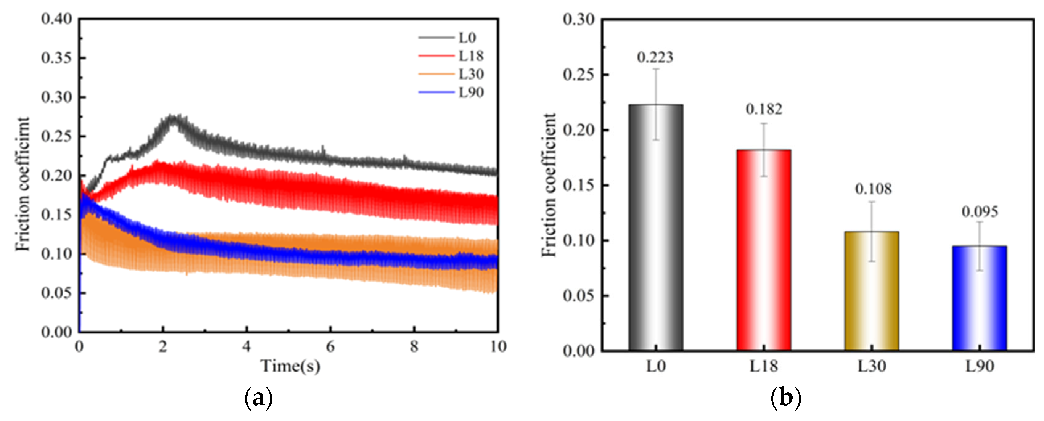
Figure 10 presents the results of friction and wear tests conducted on the Si-DLC film. In Figure 10a, it is observed that during the initial phase of friction, an oxidation reaction occurs on the surface of the Si-DLC film. This reaction increases the friction coefficient by transforming C–C and C–H bonds into C–O bonds and C=C double bonds, as noted by [29]. Subsequently, as depicted in Figure 10b, the coefficient of friction begins to decrease due to the formation of a transfer layer with very low shear strength between the two contact surfaces. As the friction process progresses, this transfer layer reaches a critical thickness, leading to the stabilization of the friction coefficient, as indicated by [30].
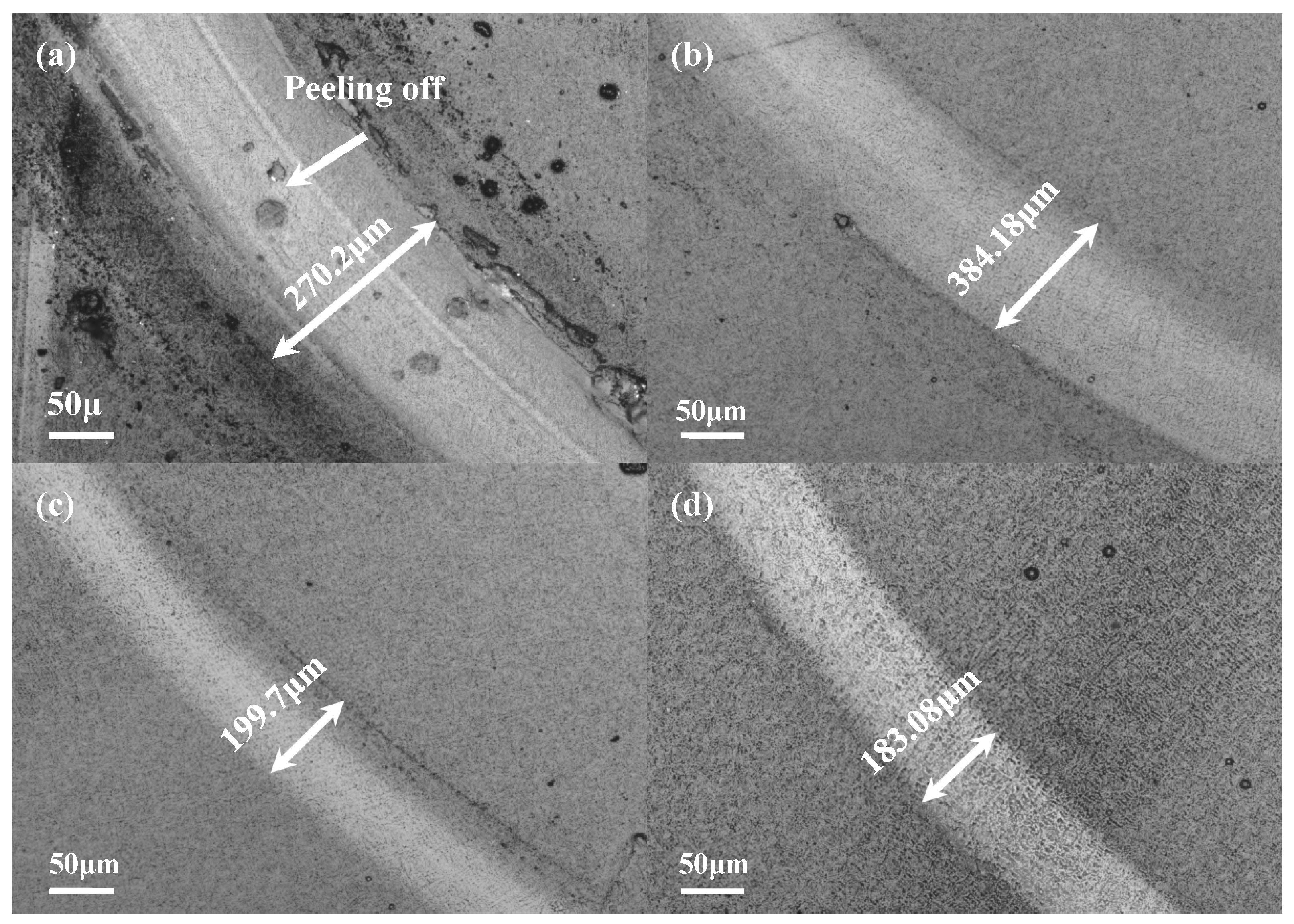
Figure 11 illustrates the microstructure of scratches on Si-DLC films. In Figure 11a, the L0 sample demonstrates peeling, with abrasion marks measuring approximately 384.18 μm in width. Conversely, Figure 11b–d reveal that the modulated films, specifically the L18, L30, and L90 samples, do not exhibit cracking or peeling, and the scratch width progressively decreases to approximately 270.2 μm, 199.7 μm, and 183.08 μm, respectively. The Si-DLC modulated films demonstrate exceptional wear resistance. This can be attributed to their dense structure and high sp3 hybridization bond content, which enhance wear resistance. The H/E and H3/E2 values are employed to assess the elastic recovery capacity and plastic deformation resistance of materials, respectively [31]. According to Leyland’s theory, a higher H3/E2 value correlates with improved wear resistance of the film [32]. As discussed, the H3/E2 value of Si-DLC modulated films is substantially greater than that of Si-DLC single-layer films, indicating their superior mechanical and tribological properties.

3.7. Corrosion Behavior

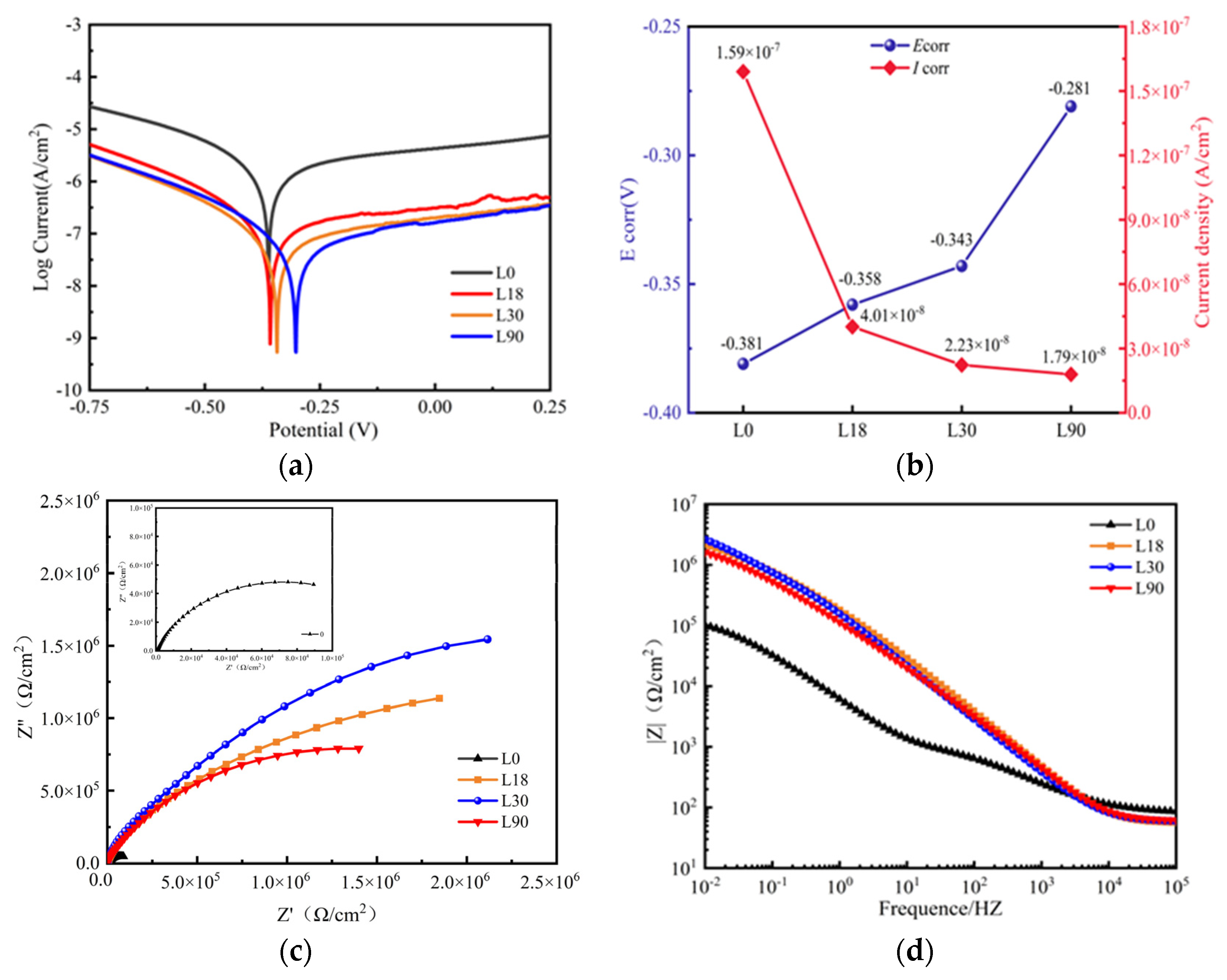
Figure 12a illustrates the dynamic potential polarization curve of the Si-DLC film, while Figure 12b presents the self-corrosion potential (Ecorr) and self-corrosion current density (icorr) as determined by the Tafel extrapolation method [33]. The Ecorr values for the bias-modulated films were −0.358 V, −0.343 V, and −0.281 V, respectively, which are all higher than that of the single-layer film at −0.381 V. Correspondingly, the icorr values for the bias-modulated films were 4.01 × 10⁻⁸ A/cm2, 2.23 × 10⁻⁸ A/cm2, and 1.79 × 10⁻⁸ A/cm2, respectively, all of which are lower than the single-layer film value of 1.59 × 10⁻⁷ A/cm2. Notably, the icorr value was reduced by an order of magnitude, indicating enhanced corrosion resistance in the modulated films. The low corrosion resistance observed in L0 samples is attributed to Cl penetration resulting from their porous structure. In contrast, for L18 and L30 samples, bias bombardment promotes film layer densification and mitigates columnar structural characteristics, leading to films with a more uniform structure. For the L90 sample, ion bombardment of the biased layer also impacts the unbiased layer due to ion penetration, resulting in a further reduction in columnar structural features and the complete elimination of layered structures. This process leads to a more uniform film structure and reduced surface porosity, effectively blocking the channels for Cl ions to penetrate the interior, thereby playing a crucial role in preventing Cl diffusion into the base material.
Figure 12c presents the Electrochemical Impedance Spectroscopy (EIS) results for the Si-DLC film. It is well established that a larger radius of the Nyquist curve semicircle indicates enhanced corrosion resistance of the samples [34]. Compared to single-layer Si-DLC films, the modulated films exhibit a larger semicircular radius and significantly improved corrosion resistance. The impedance modulus |Z| serves as an indicator of the film’s density in the high-frequency range, while in the low-frequency range, |Z| is associated with corrosion resistance. Figure 12d presents the Bode plot, which demonstrates a consistent downward trend across all samples. Notably, the |Z| value at low frequencies (|Z|f→0.01) increases with the number of modulation layers. Specifically, the |Z|f→0.01 values for L0, L18, L30, and L90 are 1.01 × 10⁵ Ω/cm2, 1.61 × 10⁶ Ω/cm2, 2.17 × 10⁶ Ω/cm2, and 2.62 × 10⁶ Ω/cm2, respectively. The |Z|f→0.01 of the modulated film is an order of magnitude greater than that of the single-layer film. A higher |Z|f→0.01 signifies enhanced stability of the passive film and improved corrosion resistance [35]. It is evident that by increasing the number of modulation layers, the impedance value is significantly enhanced, thereby corroborating the superior corrosion protection afforded by the L90 sample.

4. Conclusions

The biased modulation of Si-DLC multilayer film structures, through biased bombardment, enhances film density while reducing film thickness as the modulation period increases. The action area of biased layer bombardment particles encompasses the entire unbiased layer. This process results in a microstructural transformation, where the growth characteristics of the columnar structure are diminished, the layered structure is completely eliminated, and there is a notable increase in film density, the ID/IG value, and the number of sp3 bonds. The multilayer film structures exhibit enhanced resistance to crack propagation, as demonstrated by increased hardness and elastic modulus of the film layers, with the adhesive strength between the film and substrate rising from 34 N to 46 N. Consequently, this reduces the peeling of Si-DLC films, enhances their resistance to friction and wear, and meets the requirements for reduced friction, wear resistance, and extended service life of the workpiece. The densified structure of the Si-DLC multilayer film significantly improves its resistance to corrosion in 3.5 wt% NaCl solution. Specifically, the corrosion current of the L90 Si-DLC multilayer film is reduced by an order of magnitude compared to that of the Si-DLC single-layer film.

Author Contributions

M.G.: conceptualization, methodology, investigation, data curation, writing—original draft. H.L.: investigation, writing—original draft. M.W.: supervision, conceptualization, funding acquisition, writing—review and editing. P.L.: formal analysis, validation, writing—review and editing. All authors have read and agreed to the published version of the manuscript.

Funding

The authors gratefully acknowledge the financial support from project of Heilongjiang Provincial Department of Education, China (2018-KYYWF-0921). This work was also supported by Liaoning Provincial Fundamental Research Funds for Higher Education Institutions (LJ-212510142015).

Data Availability Statement

Data will be provided upon reasonable request.

Acknowledgments

The authors would like to thank Tian (Harbin Institute of Technology) for providing the determination of Raman spectra and XPS analysis.

Conflicts of Interest

The authors declare no conflicts of interest .

References

  1. Li, H.; Liu, L.; Guo, P.; Sun, L.; Wei, J.; Liu, Y.; Li, S.; Wang, S.; Lee, K.-R.; Ke, P.; et al. Long-term tribocorrosion resistance and failure tolerance of multilayer carbon-based coatings. Friction 2022, 10, 1707–1721. [Google Scholar] [CrossRef]
  2. Wu, Y.; Li, K.; Shi, B.; Qi, J.; Zhou, X.; Wang, Y.; Zheng, K.; Liu, Y.; Yu, S. The effect of sputtering power on the structural and tribological behaviors at elevated temperature of Ta/Si co-doped DLC films. Surf. Coat. Technol. 2024, 482, 130688. [Google Scholar] [CrossRef]
  3. Wei, X.; Chen, L.; Zhang, M.; Lu, Z.; Zhang, G. Effect of dopants (F, Si) material on the structure and properties of hydrogenated DLC film by plane cathode PECVD. Diam. Relat. Mater. 2020, 110, 108102. [Google Scholar] [CrossRef]
  4. Wang, J.; Pu, J.; Zhang, G.; Wang, L. Tailoring the structure and property of silicon-doped diamond-like carbon films by controlling the silicon content. Surf. Coat. Technol. 2013, 235, 326–332. [Google Scholar] [CrossRef]
  5. Wu, Y.; Shi, B.; Liu, Y.; Wang, L.; Gao, J.; Shen, Y.; Wang, Y.; Ma, Y.; Yu, S. Design of Ta gradient layer to improve adhesion strength between Cu substrate and DLC film. Vacuum 2022, 203, 111221. [Google Scholar] [CrossRef]
  6. Flege, S.; Hatada, R.; Ensinger, W.; Baba, K. Improved adhesion of DLC films on copper substrates by preimplantation. Surf. Coat. Technol. 2014, 256, 37–40. [Google Scholar] [CrossRef]
  7. Arslan, A.; Masjuki, H.H.; Varman, M.; Kalam, M.A.; Quazi, M.M.; Al Mahmud, K.; Gulzar, M.; Habibullah, M. Effects of texture diameter and depth on the tribological performance of DLC coating under lubricated sliding condition. Appl. Surf. Sci. 2015, 356, 1135–1149. [Google Scholar] [CrossRef]
  8. Polaki, S.R.; Kumar, N.; Ganesan, K.; Madapu, K.; Bahuguna, A.; Kamruddin, M.; Dash, S.; Tyagi, A.K. Tribological behavior of hydrogenated DLC film: Chemical and physical transformations at nano-scale. Wear 2015, 338–339, 105–113. [Google Scholar] [CrossRef]
  9. Modabberasl, A.; Kameli, P.; Ranjbar, M.; Salamati, H.; Ashiri, R. Fabrication of DLC thin films with improved diamond-like carbon character by the application of external magnetic field. Carbon 2015, 94, 485–493. [Google Scholar] [CrossRef]
  10. Forsich, C.; Dipolt, C.; Heim, D.; Mueller, T.; Gebeshuber, A.; Holecek, R.; Lugmair, C. Potential of thick a-C:H:Si films as substitute for chromium plating. Surf. Coat. Technol. 2014, 241, 86–92. [Google Scholar] [CrossRef]
  11. He, D.; Feng, Z.; Liang, R.; Wang, Q.; Shang, L. Effect of Cr3C2 content on the tribo-corrosion behaviors of Cr3C2-NiCr/DLC duplex coatings. Surf. Coat. Technol. 2024, 489, 131134. [Google Scholar] [CrossRef]
  12. He, D.; Liang, R.; Wang, Q.; Shang, L. Impact damage behaviors of Cr3C2-NiCr/DLC duplex coatings. Tribol. Inter. 2024, 200, 110086. [Google Scholar] [CrossRef]
  13. Liang, S.; He, D.; Shang, L.; Li, W.; Zhang, C.; Shao, L.; Seniuts, U.; Viktor, Z. Effect of cermet interlayer on the electrochemical behavior of Cr3C2-NiCr/DLC duplex coating. Surf. Coat. Technol. 2023, 469, 129813. [Google Scholar] [CrossRef]
  14. Wei, R. Development of new technologies and practical applications of plasma immersion ion deposition (PIID). Surf. Coat. Technol. 2010, 204, 2869–2874. [Google Scholar] [CrossRef]
  15. Azzi, M.; Amirault, P.; Paquette, M.; Klemberg-Sapieha, J.E.; Martinu, L. Corrosion performance and mechanical stability of 316L/DLC coating system: Role of interlayers. Surf. Coat. Technol. 2010, 204, 3986–3994. [Google Scholar] [CrossRef]
  16. Chicot, D.; Puchi-Cabrera, E.S.; Decoopman, X.; Roudet, F.; Lesage, J.; Staia, M.H. Diamond-like carbon film deposited on nitrided 316L stainless steel substrate: A hardness depth-profile modeling. Diam. Relat. Mater. 2011, 20, 1344–1352. [Google Scholar] [CrossRef]
  17. Jellesen, M.S.; Christiansen, T.L.; Hilbert, L.R.; Møller, P. Erosion–corrosion and corrosion properties of DLC coated low temperature gas-nitrided austenitic stainless steel. Wear 2009, 267, 1709–1714. [Google Scholar] [CrossRef]
  18. Dalibón, E.L.; Heim, D.; Forsich, C.; Rosenkranz, A.; Guitar, M.A.; Brühl, S.P. Characterization of thick and soft DLC coatings deposited on plasma nitrided austenitic stainless steel. Diam. Relat. Mater. 2015, 59, 73–79. [Google Scholar] [CrossRef]
  19. Sun, W.; Li, M.; Wu, M.; Hu, J. Uniformity of Si-containing diamond-like carbon films deposited at different positions by mesh hollow cathode discharge. Results Phys. 2019, 14, 102480. [Google Scholar] [CrossRef]
  20. Li, F.; Zhang, S.; Kong, J.; Zhang, Y.; Zhang, W. Multilayer DLC coatings via alternating bias during magnetron sputtering. Thin Solid Films 2011, 519, 4910–4916. [Google Scholar] [CrossRef]
  21. Kardar, M.; Parisi, G.; Zhang, Y.C. Dynamic Scaling of Growing Interfaces. Phys. Rev. Lett. 1986, 56, 889–892. [Google Scholar] [CrossRef]
  22. Bendavid, A.; Martin, P.J.; Comte, C.; Preston, E.W.; Haq, A.; Ismail, F.M.; Singh, R. The mechanical and biocompatibility properties of DLC-Si films prepared by pulsed DC plasma activated chemical vapor deposition. Diam. Relat. Mater. 2007, 16, 1616–1622. [Google Scholar] [CrossRef]
  23. Cui, W.G.; Lai, Q.B.; Zhang, L.; Wang, F.M. Quantitative measurements of sp3 content in DLC films with Raman spectroscopy. Surf. Coat. Technol. 2010, 205, 1995–1999. [Google Scholar] [CrossRef]
  24. Catherine, Y.; Zamouche, A. Glow discharge deposition of tetramethylsilane films. Plasma Chem. Plasma Process. 1985, 5, 353–368. [Google Scholar] [CrossRef]
  25. Ahmed, M.H.; Byrne, J.A.; McLaughlin, J.A.D.; Elhissi, A.; Ahmed, W. Comparison between FTIR and XPS characterization of amino acid glycine adsorption onto diamond-like carbon (DLC) and silicon doped DLC. Appl. Surf. Sci. 2013, 273, 507–514. [Google Scholar] [CrossRef]
  26. Irmer, G.; Dorner-Reisel, A. Micro-Raman Studies on DLC coatings. Adv. Eng. Mater. 2005, 7, 694–705. [Google Scholar] [CrossRef]
  27. Lifshitz, Y.; Kasi, S.R.; Rabalais, J.W.; Eckstein, W. Subplantation model for film growth from hyperthermal species. Phys. Rev. B 1990, 41, 10468–10480. [Google Scholar] [CrossRef]
  28. Müller, I.C.; Sharp, J.; Rainforth, W.M.; Hovsepian, P.; Ehiasarian, A. Tribological response and characterization of Mo–W doped DLC coating. Wear 2017, 376–377, 1622–1629. [Google Scholar] [CrossRef]
  29. Li, H.; Xu, T.; Wang, C.; Chen, J.; Zhou, H.; Liu, H. Tribochemical effects on the friction and wear behaviors of diamond-like carbon film under high relative humidity condition. Tribol. Lett. 2005, 19, 231–238. [Google Scholar] [CrossRef]
  30. Liu, Y.; Erdemir, A.; Meletis, E.I. An investigation of the relationship between graphitization and frictional behavior of DLC coatings. Surf. Coat. Technol. 1996, 86–87, 564–568. [Google Scholar] [CrossRef]
  31. Wang, L.; Li, L.; Kuang, X. Effect of substrate bias on microstructure and mechanical properties of WC-DLC coatings deposited by HiPIMS. Surf. Coat. Technol. 2018, 352, 33–41. [Google Scholar] [CrossRef]
  32. Leyland, A.; Matthews, A. On the significance of the H/E ratio in wear control: A nanocomposite coating approach to optimised tribological behaviour. Wear 2000, 246, 1–11. [Google Scholar] [CrossRef]
  33. Zhang, X.; Xiao, G.; Jiang, C.; Liu, B. Influence of process parameters on microstructure and corrosion properties of hopeite coating on stainless steel. Corros. Sci. 2015, 94, 428–437. [Google Scholar] [CrossRef]
  34. Li, H.T.; Sun, P.F.; Cheng, D.H.; Liu, Z.M. Effects of deposition temperature on structure, residual stress and corrosion behavior of Cr/TiN/Ti/TiN films. Ceram. Int. 2021, 47, 34909–34917. [Google Scholar] [CrossRef]
  35. Wang, Z.M.; Zhang, J.; Han, X.; Li, Q.F.; Wang, Z.L.; Wei, R. Corrosion and salt scale resistance of multilayered diamond-like carbon film in CO2 saturated solutions. Corros. Sci. 2014, 86, 261–267. [Google Scholar] [CrossRef]
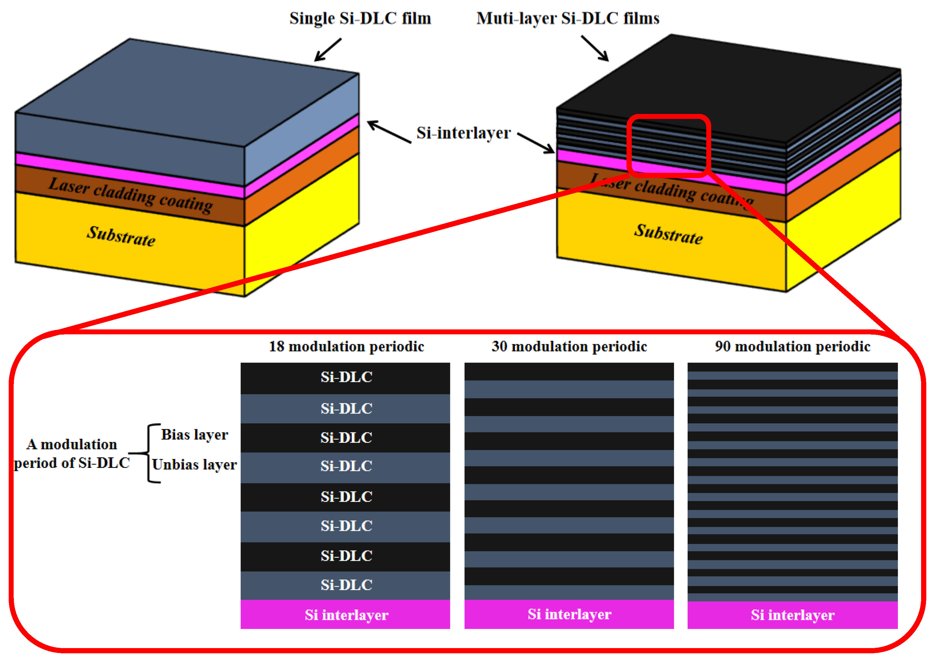
Figure 1. Schematic diagram of the muti-layer Si-DLC modulation film structure.
Coatings 15 00930 g001
Figure 2. Surface images of Si-DLC films. (a) L0, (b) L18, (c) L30, (d) L90.
Coatings 15 00930 g002
Figure 3. Cross-sectional images of Si-DLC films. (a,e) L0, (b,f) L18, (c,g) L30, (d,h) L90.
Coatings 15 00930 g003
Figure 4. The 2D AFM surface morphology of the films. (a) L0, (b) L18, (c) L30, (d) L90.
Coatings 15 00930 g004
Figure 5. Raman spectra and ID/IG ratio of Si-DLC films. (a) Raman spectra, (b) ID/IG ratio.
Coatings 15 00930 g005
Figure 6. XPS spectrum of the Si-DLC films. (ad) L0-L90 C1s spectra, (e) XPS survey, (f) sp3/sp2 ratio.
Coatings 15 00930 g006aCoatings 15 00930 g006b
Figure 7. Schematic diagram of ion bombardment area.
Coatings 15 00930 g007
Figure 8. Nanohardness and modulus as well as H/E and H3/E2 of Si-DLC films load-depth curves: (a) Depth-Load curve, (b) nanohardness, (c) elastic modulus, (d) H/E and H3/E2.
Coatings 15 00930 g008
Figure 9. Scratch images of the Si-DLC films. (a) L0, (b) L18, (c) L30, (d) L90.
Coatings 15 00930 g009
Figure 10. Friction and wear results of the Si-DLC films friction and wear curves; (a) friction coefficient curve, (b) friction coefficient.
Coatings 15 00930 g010
Figure 11. Features of wear tracks of Si-DLC films. (a) L0, (b) L18, (c) L30, (d) L90.
Coatings 15 00930 g011
Figure 12. Electrochemical corrosion results of Si-DLC films in 3.5% Nacl solution. (a) Tafel curves, (b) Ecorr and Icorr, (c) Nyquist plots, (d) Bode plots.
Coatings 15 00930 g012
Table 1. The chemical composition and content of commercial powders (wt%).
ElementCBSiCrNiMnMoWCFe
Content0.180.840.9018.374.250.544.340.54Bal
Table 2. The detailed parameters for depositing the multilayer Si-DLC modulation films.
FilmProcessArTMSC2H2VoltageCurrentBiasTimeModulation Period
SccmVAVMin
L0Clean200//140045−200300
Si-interlayer20020/140060010
Si-DLC70101301350800/−200180
L18Clean200//140045−2003018
Si-interlayer20020/140060010
Si-DLC70101301350800/−200180
L30Clean200//140045−2003030
Si-interlayer20020/140060010
Si-DLC70101301350800/−200180
L90Clean200//140045−2003090
Si-interlayer20020/140060010
Si-DLC70101301350800/−200180
Disclaimer/Publisher’s Note: The statements, opinions and data contained in all publications are solely those of the individual author(s) and contributor(s) and not of MDPI and/or the editor(s). MDPI and/or the editor(s) disclaim responsibility for any injury to people or property resulting from any ideas, methods, instructions or products referred to in the content.