Article

385 nm AlGaN Near-Ultraviolet Micro Light-Emitting Diode Arrays with WPE 30.18% Realized Using an AlN-Inserted Hole Spreading Enhancement S Electron Blocking Layer

1
Institute of Next Generation Semiconductor Materials, Southeast University, Suzhou 215123, China
2
Department of Electrical and Electronic Engineering, School of Advanced Technology, Xi’an Jiaotong-Liverpool University, Suzhou 215123, China
*
Author to whom correspondence should be addressed.
Coatings 2025, 15(8), 910; https://doi.org/10.3390/coatings15080910 (registering DOI)
Submission received: 30 June 2025 / Revised: 31 July 2025 / Accepted: 1 August 2025 / Published: 3 August 2025

Abstract

In this work, we demonstrate high-efficiency 385 nm AlGaN-based near-ultraviolet micro light emitting diode (NUV-Micro LED) arrays. The epi structure is prepared using a novel AlN-inserted superlattice electrical blocking layer which enhances hole spreading in the p-type region significantly. The NUV-Micro LED arrays in this work comprise 228 chips in parallel with wavelengths at 385 nm, and each single chip size is 15 × 30 μm2. Compared with conventional bulk AlGaN-based EBL structures, the NUV-Micro LED arrays that implemented the new hole spreading enhanced superlattice electrical blocking layer (HSESL-EBL) structure proposed in this work had a remarkable increase in light output power (LOP) at current density, increasing the range down from 0.02 A/cm2 to as high as 97 A/cm2. The array’s light output power is increased up to 1540% at the lowest current density 0.02 A/cm2, and up to 58% at the highest current density 97 A/cm2, measured under room temperature (RT); consequently, the WPE is increased from 13.4% to a maximum of 30.18%. This AlN-inserted HESEL-EBL design significantly enhances both the lateral expansion efficiency and the hole injection efficiency into the multi quantum well (MQW) in the arrays, improving the concentration distribution of the holes in MQW while maintaining good suppression of electron leakage. The array’s efficiency droop has also been greatly reduced.

1. Introduction

Ultraviolet light-emitting diodes (UV LEDs) are extensively researched for applications including water/air disinfection, medical esthetics, and non-line-of-sight communication. Their wavelength tunability, low power consumption, and environmental sustainability position them as a leading alternative to mercury lamps [1]. Notably, high-efficiency near-ultraviolet (NUV) LEDs (360–385 nm) show significant potential in niche markets such as UV curing, medical devices, 3D printing resin curing, and quantum dot excitation [2,3]. Unlike conventional high-power UV systems, these applications prioritize photoelectric conversion efficiency at micro-scale sizes and ultra-low current densities [4]. AlGaN-based semiconductors, with tunable bandgaps enabling precise UV wavelength control (220–405 nm), are pivotal for ensuring high-performance UV optoelectronics [5,6]. However, AlGaN-based NUV-Micro LEDs still face challenges in terms of light output power and efficiency compared to commercial InGaN-based visible LEDs, primarily due to low external quantum efficiency (EQE) [7,8]. Since EQE correlates directly with wall-plug efficiency (WPE), this study evaluates device performance using WPE as a proxy for EQE [9].
The low internal quantum efficiency (IQE) and light extraction efficiency (LEE) of ultraviolet light-emitting diodes (UV-LEDs) are key contributors to their poor external quantum efficiency (EQE) and wall-plug efficiency (WPE) [10]. While AlGaN/InAlGaN quantum wells (QWs) with emission wavelengths of 360–405 nm (near-ultraviolet, NUV) theoretically achieve IQE values of 70%–80% [11], practical NUV-LED devices exhibit WPE values below 15%, significantly lower than those of commercial InGaN blue LEDs [12]. This gap stems from the following:
  • Low carrier injection efficiency (CIE): Electron leakage from QWs, exacerbated by insufficient hole concentrations and poor lateral spreading in p-type AlGaN layers [13,14].
  • Material limitations: High Al composition in AlGaN barriers and electron-blocking layers (EBLs) improves CIE but introduces spontaneous/piezoelectric polarization effects in p-AlGaN. These effects increase Mg-H activation energy, hindering hole concentration enhancement compared to p-GaN [6,15,16,17].
  • Imbalanced carrier distribution: Reduced wavefunction overlap due to uneven electron–hole injection into the active region [18,19], coupled with severe electron leakage into the p-type region from low hole concentrations [20,21,22].
Collectively, these factors—electron overflow, inefficient hole transport, and AlGaN’s wide bandgap-induced high activation energy—restrict the NUV-LED WPE to sub-15% levels [23,24].
To enhance the WPE of near-ultraviolet light-emitting diodes (NUV-LEDs), researchers have proposed innovative electron-blocking layer (EBL) designs, band structure engineering, and quantum barrier (QB) configurations to improve carrier injection efficiency (CIE) [25,26,27]. Simulations demonstrate that these approaches—including graded superlattice (SL) structures, asymmetric step quantum barriers, and Si-doped quantum barriers—effectively suppress electron overflow from quantum wells to the p-type region [28,29,30,31]. For instance, advanced EBL architectures such as linear Al-gradient EBLs, step-graded superlattices, and inverted-V-shaped Al composition profiles enhance electron–hole wavefunction overlap and device performance [32,33,34,35,36,37,38,39,40]. However, existing studies predominantly focus on theoretical models, with limited experimental validation of fine-tuned EBL variations in NUV epitaxial wafers or micro-scale chips. Systematic experimental validation and in-depth mechanistic analysis of EBL structures remain critical for confirming their practical efficacy in NUV-LEDs. C.K. Wang’s simulation study demonstrated that introducing a high-Al-composition interlayer between the MQW region and the EBL can effectively mitigate efficiency degradation while enhancing optical output power and IQE [41]. However, incorporating such high-Al-content layers significantly increases the complexity of epitaxial growth and may compromise crystal quality due to lattice mismatch and growth challenges [42]. Zhiyuan Liu et al. proposed a polarization-modulated InAlN last quantum barrier (LQB) design with Indium compositions ranging from 0.14 to 0.16 for 320 nm UVB LEDs. By tailoring the polarization at the LQB/EBL interface using InAlN, their simulation achieved a 32% improvement in IQE and WPE of 7.52% [43]. Despite these promising results, the experimental realization of high-Al-composition AlGaN or AlN thin layers remains technically challenging due to the difficulties in growing high-quality films at relatively low temperatures (<1000 °C). Mohd Ann et al. developed a 388 nm NUV-LED using an InGaN/GaN/AlxGa1−xN/GaN MQW structure, achieving a WPE of up to 14% [44]. However, to accommodate for the low growth temperatures required by the quantum well, the Al content in the AlGaN layer was limited to less than 5%, which constrains the broader applicability of this approach. Chaozhi Xu et al. reported that inserting an undoped AlGaN layer of appropriate thickness between the LQB and EBL in a 398 nm device led to significant improvements in both light output power and quantum efficiency, with a remarkable WPE of 50% achieved while keeping the Al content below 15% [45]. Nonetheless, the performance impact of inserting a high-quality AlN layer within the EBL structure at elevated temperatures (e.g., ~950 °C), especially for shorter-wavelength NUV-LEDs, remains largely unexplored and warrants further investigation [46].
In this work, we propose a new AlN-inserted Hole Spreading Enhanced Superlattice Electron Blocking Layer structure design, using an AlN insertion transition layer combined with an A l x G a 1 x N / G a N superlattice structure. The photoelectric performance parameters under low and high current densities are compared with traditional SL-EBL structures and graded superlattice EBLs. By performing a detailed analysis of light output power and photoelectric conversion efficiency at micro sizes and extremely low current densities, the mechanisms of hole carrier lateral spreading efficiency and transport efficiency can be thoroughly investigated. The EBL structure designed in this work consists of a graded superlattice A l 0.15 0.12 G a N / G a N layer, with an AlN interval-inserted expansion layer, and two groups of nested heavy Mg-doping p-GaN. We also investigated the effects of using HSESL-EBL on the WPE/EQE values of the NUV-Micro LED arrays. The AlN-inserted HSESL-EBL creates an effective barrier height, significantly suppressing electron leakage and improving hole transport efficiency in NUV-Micro LED arrays, particularly at low current densities. The experimental results show that this AlN-inserted HSESL-EBL can provide the “effective barrier height” and thus significantly reduces electron leakage in NUV-Micro LED arrays, thereby enhancing hole transport efficiency, especially under low current density operation mode. NUV-Micro LED arrays of 385 nm using this structure successfully achieved record high WPE and light output power (LOP) and show a significant improvement in the efficiency droop effect.

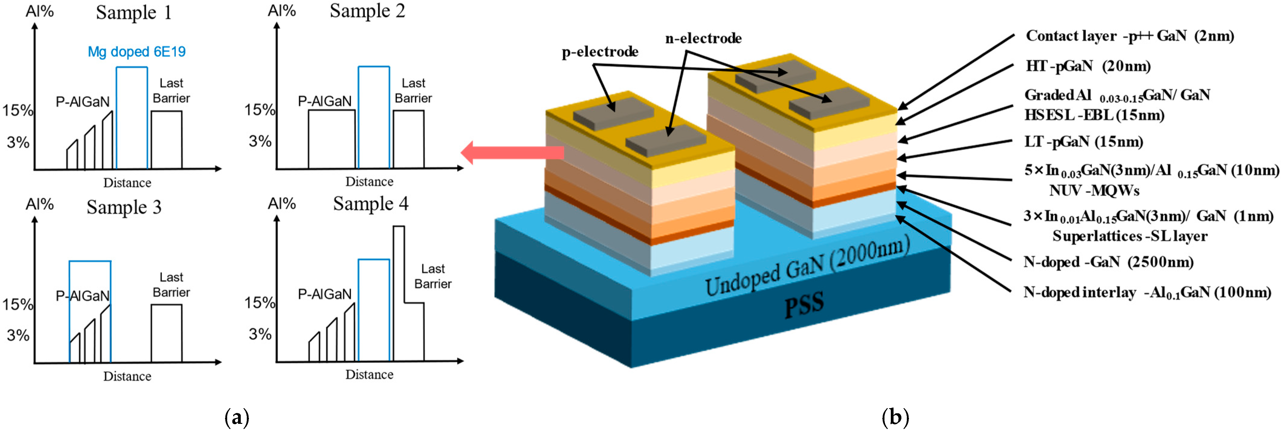
2. Device Structures and Parameters

In this study, four near-ultraviolet micro-light-emitting diode chip array samples with identical epitaxial layers (except EBL variations) were fabricated on 4-inch patterned sapphire substrates (PSSs) to isolate the EBL effects. The growth process was as follows: Initially, a 15 nm thick aluminum nitride (AlN) nucleation layer was deposited on a C-plane 4-inch PSS using physical vapor deposition (PVD). Subsequently, the following layers were sequentially grown on the AlN template via K465i Veeco metal–organic chemical vapor deposition (MOCVD): trimethyl–gallium (TMGa), trimethyl–aluminum (TMAl), trimethylindium (TMIn), bis-cyclopentadienyl magnesium (Cp2Mg), disilane (Si2H6), and ammonia (NH3), used as the Ga, Al, In, Mg, Si, and N sources, respectively.
  • The substrate was cleaned in H2 ambient at a temperature of 1080 °C for 8 min to remove any impurities and oxygen.
  • A 3 μm thick n-type GaN layer with a silicon doping concentration of 2 × 1019 cm−3; grown at 1070 °C with a V/III ratio of 4000.
  • There was a 9 Loops period active region, and each pair was composed of 3 nm In0.02GaN quantum wells (QWs) + 12 nm Al0.15GaN barrier layer (N-type doping 2 × 1017 cm−3) with Al composition equal to 15%, grown at 900 °C with an identical V/II ratio of 33,000 to prevent fluctuations of the temperature during the growth of active layers.
  • A 20 nm p-type Al0.15GaN EBL (Mg: 2 × 1018 cm−3) grown at 930 °C with a V/III ratio of 800 and four different EBL structures, namely sample 1, 2, 3, and 4, to investigate the effect of EBL on the structure of NUV-LEDs.
  • A 20 nm p-type GaN HSESL (Mg: 6 × 1019 cm−3) followed with a V/III ratio of 5000 at 950 °C.
  • A 2 nm p-type GaN contact layer (Mg: 2.5 × 1020 cm−3) with the same growth condition of the p-type GaN HSESL layer.
The four samples exhibited distinct Al composition profiles: conventional EBL structures or HSEL-EBL composite architectures embedded within AlN key design. The specific designs were as follows:
  • Sample 1: Graded Al EBL (3%→15%, linear) + dual Mg doping peaks.
  • Sample 2: Uniform Al EBL (15%) + dual Mg peaks.
  • Sample 3: Graded Al EBL + single Mg peak with polarization doping for enhanced hole concentration.
  • Sample 4: AlN-inserted HSESL-EBL composite (graded Al + dual Mg peaks).
The Al composition profiles and the whole structure of the samples are illustrated in Figure 1a,b.
Following epitaxy, flip-chip technology was employed to fabricate the NUV-Micro LED arrays as shown in Figure 2a,b [47]. Both p-type and n-type electrodes were fabricated using Ni/Au metallization. The arrays consisted of 228 individual NUV-Micro LED pixels connected in parallel, with each pixel measuring 15 × 30 μm2. The operational current densities range of the arrays spanned from 0.02 A/cm2 to 97 A/cm2, corresponding to a single current range of 0.1 μA to 438 μA for a single pixel. Finally, the optoelectronic performance of the samples was systematically characterized under bare-chip Chip on Board (COB) conditions, including measurements of the current density–voltage (I–V) characteristics and WPE, among other critical parameters.

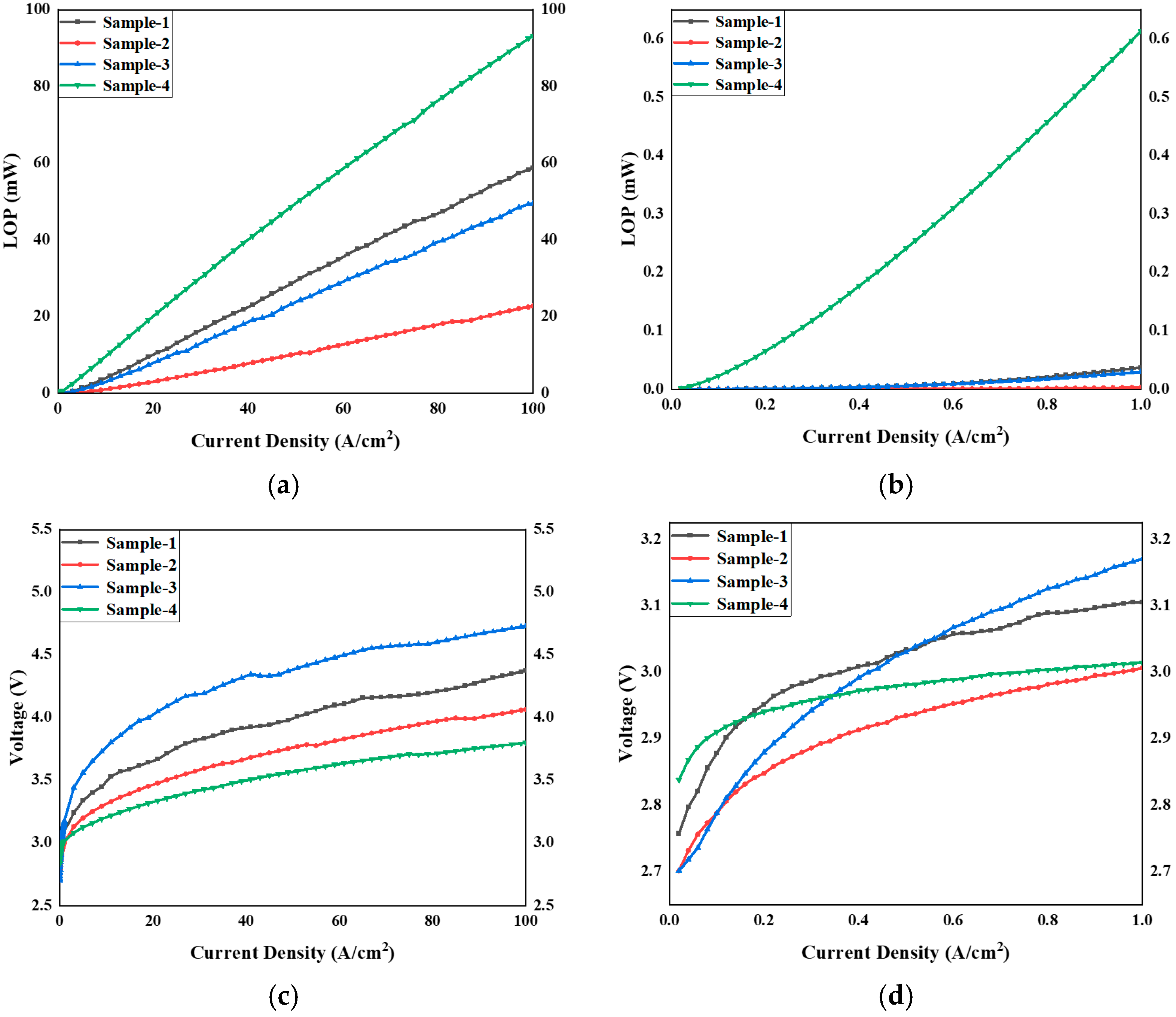
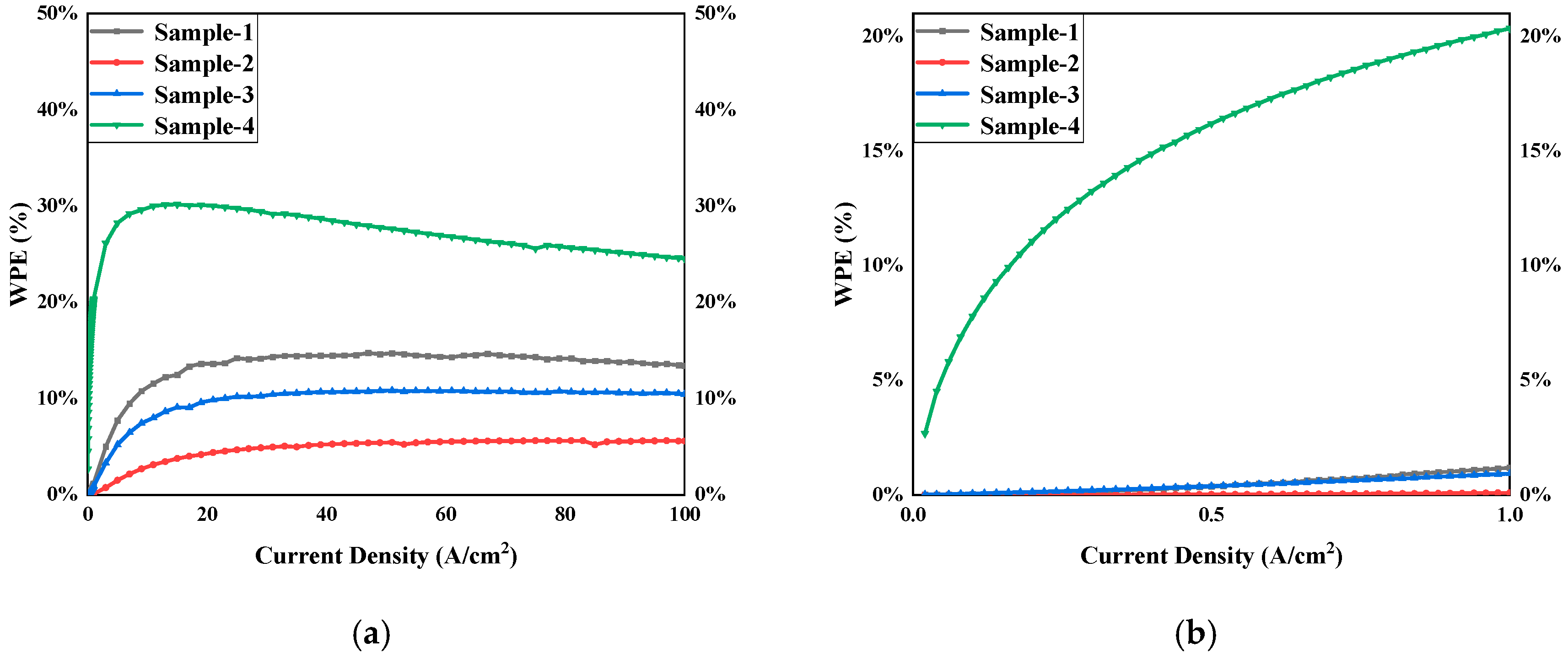
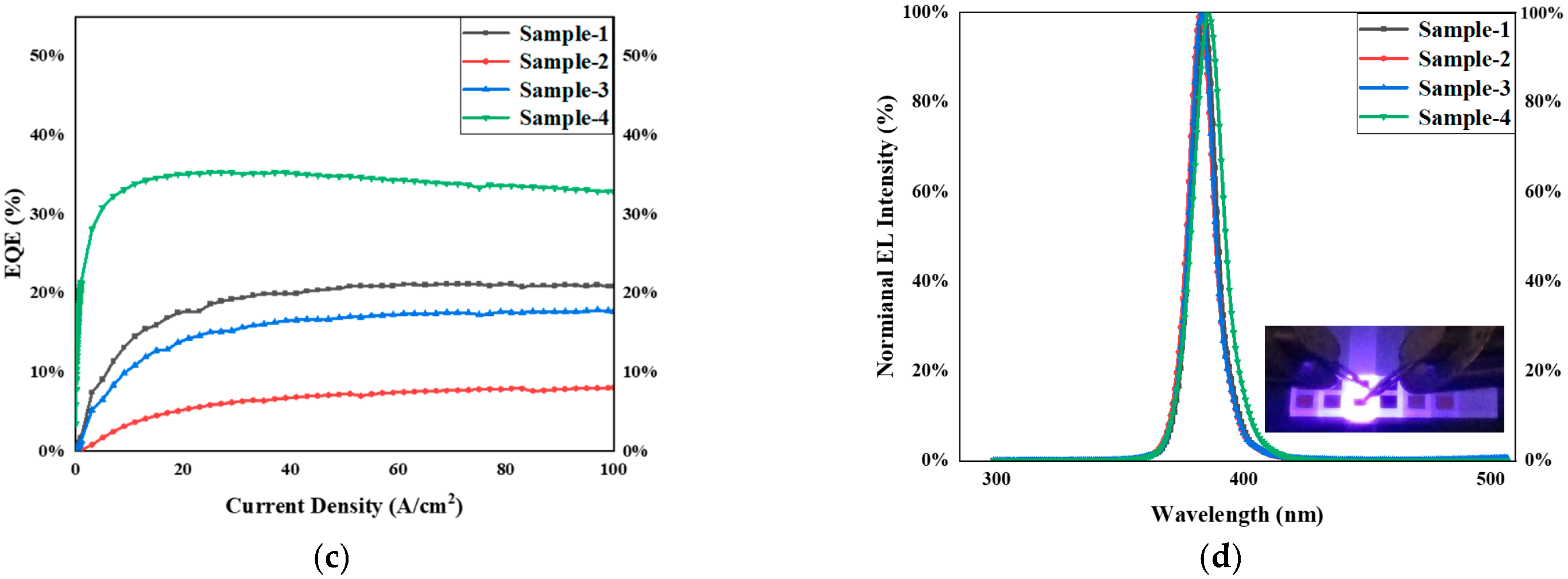
3. Results and Discussion

Figure 3 illustrates the light output power (a) (b) and current voltage (IV) characteristics (c) (d) of 385 nm AlGaN NUV-Micro LED array chips, designed with different composite EBL structures, under varying injection currents. All measurements were conducted under room temperature (RT cw) continuous-wave conditions. The relationship between the current density and light output power reveals that sample 4 exhibits a significant advantage in light output power at both low and high current densities. At low current densities, sample 4 maintains a relatively high light output power, which is an order of magnitude greater than that of the other three traditional EBL samples, as shown in Figure 3b.
Specifically, whether the EBL is composed of a graded Al composition (Graded-EBL), a constant Al composition (Constant-EBL), or a Mg-doped design with polarization doping, as the driving current density increases from 0.02 A/cm2 to 97 A/cm2, the total light output power of the device array significantly increases at low current densities, from 1.0 × 10⁻⁵ mW (at 3.08 V) for sample 1 to 1.5 × 10⁻³ mW (at 2.84 V) for sample 4. At high current densities, the total light output power increases from 58.76 mW (at 4.37 V) for sample 1 to 93.26 mW (at 3.8 V) for sample 4, as shown in Figure 3c.
The significant increase in the light output power of the device array is accompanied by a decrease in operating voltage, which directly leads to an increase in device WPE from 13.4% to a maximum of 30.18%, 180% higher than that of the other three samples, as shown in Figure 4a,b. The significant improvements in the photoelectric output power of the device array at both low and high current densities are attributed to the improvements in the NUV-Micro LED chip’s carrier concentration distribution in the UV quantum wells and the increased recombination probability of electron–hole pairs, leading to a more balanced carrier concentration distribution in the quantum well region of the device. This is particularly evident in the improvement in the hole concentration distribution and lateral spreading efficiency, while the changes in the electron concentration distribution are not significant.
The improved structure maintains the sufficient electron barrier height of the traditional EBL structure, effectively blocking excessive electron leakage into the quantum well layer and the p-type layer of the device at a micro size.
Based on the I–V characteristic curves in Figure 3, the NUV-Micro LED arrays exhibit typical diode-like behavior, with sample 4 demonstrating enhanced performance. Under identical injection current conditions, sample 4 exhibits a significantly lower voltage compared to the other samples, likely due to the gradient Al composition in the EBL. Specifically, the gradient Al’s composition induces a gradual tilt in the valence band from the high-Al end to the low-Al end within the EBL, forming a “slope” structure that facilitates hole transport and effectively reduces the hole injection barrier. This structural modification facilitates the activation of Mg acceptors, increases the hole concentration, and significantly reduces the p-type contact resistance. Furthermore, the gradient design increases the spatial distribution depth of the holes within the quantum well, thereby enhancing the radiative recombination efficiency and further reducing the overall resistance. As illustrated in the inset figure, sample 4 maintains exceptional electrical performance even at low injection currents. Moreover, at a current density of 1 A/cm2, the increase in resistance for sample 4 is notably slower compared to the other samples. These findings provide solid evidence that the proposed gradient EBL design significantly improves the electrical performance of the NUV-Micro LED arrays. This can be attributed to several factors, particularly the optimization of the carrier concentration distribution within the UV quantum wells and the increased electron–hole recombination probability, resulting in a more balanced carrier distribution within the quantum well region. Notably, the improvement in the hole concentration distribution and lateral spreading efficiency plays a critical role, leading to more uniform carrier injection into the quantum wells. While the improvement in the electron concentration distribution is relatively modest, it still contributes to the overall optimization of device performance. The modified EBL structure maintains an adequate electron potential barrier and effectively suppresses excessive electron leakage into the quantum well and p-type layers at the micron scale. This results in a significant increase in light output power, as well as a reduction in operating voltage, which together enhance the device’s optoelectronic performance.
It needs to be emphasized that for this study, the chip fabrication process and the main quantum well region’s structural design for all samples are identical, confirming that the IQE and LEE (light extraction efficiency) of the comparison group devices should remain unchanged. Therefore, the effective wall barrier of the optimized AlN-inserted HSESL-EBL structure design in this work is the primary reason for the great improvement in the light output power and WPE in the NUV-Micro LED array.

4. Conclusions

In summary, we proposed an AlN-inserted HSESL-EBL structure for use in NUV LEDs and successfully fabricated NUV-Micro LED arrays consisting of 228 NUV-Micro LED chips with a central wavelength of 385 nm, each with a size of 15 × 30 μm2, connected in parallel. The measured results show that the optimized composite EBL structure in this work results in lower voltage (by 0.2 V) and 150 times higher LOP as compared to NUV-Micro LEDs with conventional EBL structures under a low current density operation mode of 0.02 A/cm2, and 2 times higher LOP under 97 A/cm2 current density. Since the NUV-Micro LED arrays operate in this ultra-low injection current mode, the device’s photoelectric performance test results can effectively avoid the influence of electron leakage. With a consistent MQW main structure among the experimental group chips, the epi dislocation density and IQE performance of the active region are kept consistent. The significant improvement in photoelectric performance is attributed to the AlN-inserted HSESL-EBL structure design, which greatly enhances the hole lateral transport efficiency and carrier injection efficiency in the main quantum well region. This effectively proves that the optimization through the band engineering of electron and hole carriers through the EBL improves the hole injection efficiency, which optimizes the carrier concentration distribution in the main quantum well region. The optimized hole injection efficiency leads to a desired change in the carrier concentration distribution, resulting in much improved photoelectric efficiency. This enhancement of the band regulation results in a noticeable improvement in the results, whether under ultra-low current density drive or high current density drive. When the arrays operate at a current of 100 mA, the output ultraviolet power reaches 93 mW and WPE could reach 30.18%, respectively. This is currently the highest reported value in the 385 nm NUV-LED reports. However, practical constraints prevented the inclusion of band diagrams to explain the enhanced electron blocking efficiency, representing a limitation of this study. Future work will address this through band structure simulations for further theoretical validation.

Author Contributions

Conceptualization, Q.N., S.Z., J.Y., X.G.; methodology, Q.N., S.Z.; investigation, Q.N., J.Y., Y.Z.; resources, X.G., H.D., Q.F., X.N.; writing—original draft preparation, Q.N., S.Z.; writing—review and editing, X.G.; visualization, Q.N., S.Z., J.Y.; supervision, X.G.; project administration, X.G.; funding acquisition, X.G. All authors have read and agreed to the published version of the manuscript.

Funding

This research received no external funding.

Institutional Review Board Statement

Not applicable.

Informed Consent Statement

Informed consent was obtained from all subjects involved in this study.

Data Availability Statement

Data are contained within the article.

Conflicts of Interest

The authors declare no conflicts of interest.

References

  1. Pernot, C.; Fukahori, S.; Inazu, T.; Fujita, T.; Kim, M.; Nagasawa, Y.; Hirano, A.; Ippommatsu, M.; Iwaya, M.; Kamiyama, S.; et al. Development of high efficiency 255–355nm AlGaN-based light-emitting diodes. Phys. Status Solidi A-Appl. Mater. Sci. 2011, 208, 1594–1596. [Google Scholar] [CrossRef]
  2. Khan, A.; Balakrishman, K.; Katona, T. Ultraviolet light-emitting diodes based on group three nitrides. Nat. Photonics 2008, 2, 77–84. [Google Scholar] [CrossRef]
  3. Mori, M.; Hamamoto, A.; Takahashi, A.; Nakano, M.; Wakikawa, N.; Tachibana, S.; Ikehara, T.; Nakaya, Y.; Akutagawa, M.; Kinouchi, Y. Development of a new water sterilization device with a 365nm UV-LED. Med. Biol. Eng. Comput. 2007, 45, 1237–1241. [Google Scholar] [CrossRef]
  4. Hirayama, H.; Maeda, N.; Fujikawa, S.; Toyoda, S.; Kamata, N. Recent progress and future prospects of AlGaN-based high efficiency deep-ultraviolet light-emitting diodes. Jpn. J. Appl. Phys. 2014, 53, 100209. [Google Scholar] [CrossRef]
  5. Lin, W.Y.; Wang, T.Y.; Ou, S.L.; Liang, J.H.; Wuu, D.S. Improved performance of 365nm LEDs by inserting an un-doped electron blocking layer. IEEE Electron. Device Lett. 2014, 35, 467–469. [Google Scholar] [CrossRef]
  6. Won, W.S.; Tran, L.G.; Park, W.T.; Kim, K.K.; Shin, C.S.; Kim, N.; Kim, Y.J.; Yoon, Y.J. UV-LEDs for the disinfection and Bio-Sensing applications. Int. J. Precis. Eng. Manuf. 2018, 19, 1901–1915. [Google Scholar] [CrossRef]
  7. Hirayama, H.; Yatabe, T.; Noguchi, N.; Ohashi, T.; Kamata, N. 231–261nm AlGaN deep-ultraviolet light-emitting diodes fabricated on AlN multilayer buffers grown by ammonia pulse-flow method on sapphire. Appl. Phys. Lett. 2007, 91, 071901. [Google Scholar] [CrossRef]
  8. Hai, X.; Rashid, R.; Sadaf, S.; Mi, Z.; Zhao, S. Effect of low hole mobility on the efficiency droop of AlGaN nanowire deep ultraviolet light emitting diodes. Appl. Phys. Lett. 2019, 114, 101104. [Google Scholar] [CrossRef]
  9. Kneissl, M.; Kolbe, T.; Chua, C.; Kueller, V.; Lobo, N.; Stellmach, J.; Knauer, A.; Rodriguez, H.; Einfeldt, S.; Yang, Z.; et al. Advances in group III-nitride-based deep UV light-emitting diode technology. Semicond. Sci. Technol. 2011, 26, 014036. [Google Scholar] [CrossRef]
  10. Yao, Y.; Li, H.; Wang, M.; Li, P.; Lam, M.; Iza, M.; Speck, J.S.; Denbaars, S.P.; Nakamura, S. High external quantum efficiency (6.8%) UV-A LEDs on AlN templates with quantum barrier optimization. Opt. Express 2023, 31, 28649. [Google Scholar] [CrossRef] [PubMed]
  11. Tamulaitis, G. Ultraviolet Light emitting diodes. Lith. J. Phys. 2011, 51, 177–193. [Google Scholar] [CrossRef]
  12. Delaney, K.T.; Rinke, P.; Van de Walle, C.G. Auger recombination rates in nitrides from first principles. Appl. Phys. Lett. 2009, 94, 141101. [Google Scholar] [CrossRef]
  13. Li, J.; Oder, T.N.; Nakarmi, M.L.; Lin, J.Y.; Jiang, H.X. Optical and electrical properties of Mg-doped p-type AlxGa1-xN. Appl. Phys. Lett. 2002, 80, 1210. [Google Scholar] [CrossRef]
  14. Hirayama, H.; Tsukada, Y.; Maeda, T.; Kamata, N. 227nm AlGaN Light-Emitting Diode with 0.15mW Output Power Realized using a Thin quantum Well and AlN Buffer with Reduced threading dislocation Density. Appl. Phys. Express 2008, 1, 051101. [Google Scholar] [CrossRef]
  15. Nam, K.B.; Li, J.; Nakarmi, M.L.; Lin, J.Y.; Jiang, H.X. Unique optical properties of AlGaN alloys and related ultraviolet emitters. Appl. Phys. Lett. 2004, 84, 25. [Google Scholar] [CrossRef]
  16. Zhou, S.; XU, H.; HU, H.; Gui, C.; Liu, S. High quality GaN buffer layer by isoelectric doping and its application to 365 nm InGaN/AlGaN ultraviolet light-emitting diodes. Appl. Surf. Sci. 2019, 471, 231–238. [Google Scholar] [CrossRef]
  17. Hirayama, H.; Fujikawa, S.; Noguchi, N.; Norimatsu, J.; Takano, T.; Tsubaki, K.; Kamata, N. 222–282nm AlGaN and InAlGaN-based deep-UV LEDs fabricated on high-quality AlN on sapphire. Phys. Status Solidi A 2009, 206, 1176. [Google Scholar] [CrossRef]
  18. Mondal, R.K.; Chatterjee, V.; Pal, S. Efficient Carrier Transport for AlGaN-Based Deep-UV LEDs with Graded Superlattice p-AlGaN. IEEE Trans. Electron. Devices 2020, 67, 1674–1679. [Google Scholar] [CrossRef]
  19. Fiorentini, V.; Bernardini, F.; Sala, F.D.; Carlo, A.D.; Lugli, P. Effects of macroscopic polarization in III-V nitride multi-quantum-wells. Physics 1999, 60, 8849. [Google Scholar] [CrossRef]
  20. Wang, L.; Li, G.; Song, W.; Wang, H.; Luo, X.; Sun, Y.; Zhang, B.; Jiang, J.; Li, S. Improved performance of AlGaN-based near ultraviolet light-emitting diodes with convex quantum barrier. Superlattices Microstruct. 2018, 122, 608–613. [Google Scholar] [CrossRef]
  21. Lu, L.; Wan, Z.; Xu, F.; Wang, X.; Lv, C.; Shen, B.; Jiang, M.; Chen, Q. Performance improvement of AlGaN-based deep-ultraviolet light-emitting diodes via asymmetric step-like AlGaN quantum wells. Superlattices Microstruct. 2017, 104, 240–246. [Google Scholar] [CrossRef]
  22. Kuo, Y.K.; Chen, Y.H.; Chang, J.Y.; Tsai, M.C. Numerical analysis on the effects of bandgap energy and polarization of electron blocking layer in near-ultraviolet light-emitting diodes. Appl. Phys. Lett. 2012, 100, 043513. [Google Scholar] [CrossRef]
  23. Rasheed, S.; Usman, M.; Ali, S.; Mustafa, L.; Ali, H. Designing p-region of AlGaN ultraviolet light-emitting diodes for the improved performance. Phys. B 2023, 659, 414865. [Google Scholar] [CrossRef]
  24. Tian, W.; Feng, Z.H.; Liu, B.; Xiong, H.; Zhang, J.B.; Dai, J.N.; Cai, S.J.; Chen, C.Q. Numerical study of the advantages of ultraviolet light-emitting diodes with a single step quantum well as the electron blocking layer. Opt. Quantum Electron. 2013, 45, 381–387. [Google Scholar] [CrossRef]
  25. Chen, Y.; Song, H.; Li, D.; Sun, X.; Jiang, H.; Li, Z.; Miao, G.; Zhang, Z.; Zhou, Y. Influence of the growth temperature of AlN nucleation layer on AlN template grown by high-temperature MOCVD. Mater. Lett. 2014, 114, 26–28. [Google Scholar] [CrossRef]
  26. Hirayama, H.; Tsukada, Y.; Maeda, T.; Kamata, N. Marked enhancement in the efficiency of Deep-Ultraviolet AlGaN Light-Emitting Diodes by Using a Multiquantum-Barrier Electron Blocking layer. Appl. Phys. Express 2010, 3, 031002. [Google Scholar] [CrossRef]
  27. He, C.; Zhao, W.; Zhang, K.; He, L.; Wu, H.; Liu, N.G.; Zhang, S.; Liu, X.; Chen, Z. High-Quality GaN Epilayers Achieved by Facet-Controlled Epitaxial Lateral Overgrowth on Sputtered AlN/PSS Templates. ACS Appl. Mater. Interfaces 2017, 9, 43386–43392. [Google Scholar] [CrossRef]
  28. Jiang, Z.; Zhu, Y.; Xia, C.; Sheng, Y.; Li, Y. Enhanced characteristics in AlGaN-based deep ultraviolet light-emitting diodes with interval-graded barrier superlattice electron blocking layers. Micro Nanostruct. 2024, 191, 207869. [Google Scholar] [CrossRef]
  29. Khan, M.A.; Maeda, N.; Rangaraju, H.; Jo, M.; Iimura, K.; Hirayama, H. Efficiency droop in AlGaN crystal-based UVB LEDs in the context of electron blocking mechanism. J. Cryst. Growth 2023, 604, 127032. [Google Scholar] [CrossRef]
  30. Shi, L.; Du, P.; Tao, G.; Liu, Z.; Luo, W.; Liu, S.; Zhou, S. High efficiency electron-blocking-layer-free ultraviolet LEDs with graded Al-content AlGaN insertion layer. Superlattices Microstruct. 2021, 158, 107020. [Google Scholar] [CrossRef]
  31. Wang, W.; Chu, C.; Che, J.; Hang, S.; Shao, H.; Tian, K.; Zhang, Y.; Zhang, Z. Is a thin p-GaN layer possible for making high-efficiency AlGaN-based deep-ultraviolet light-emitting diodes? Opt. Express 2021, 29, 29651. [Google Scholar] [CrossRef] [PubMed]
  32. Li, G.; Song, W.; Wang, H.; Luo, X.; Li, S. Performance improvement of UV light-emitting diodes with triangular quantum barriers. IEEE Photonics Technol. Lett. 2018, 30, 1071–1074. [Google Scholar] [CrossRef]
  33. Wang, X.; Sun, H.Q.; Yang, X.; Yi, X.Y.; Sun, J.; Zhang, X.; Liu, T.Y.; Guo, Z.Y.; Zhao, L.Z. Performance enhancement of AlGaN-based UV-LEDs inserted with a pin-doped AlGaN layer between the active region and electron-blocking layer. Mater. Sci. Semicond. Process. 2018, 83, 133–138. [Google Scholar] [CrossRef]
  34. Liu, N.; Gu, H.; Wei, Y.; Zheng, S. Performance enhancement of AlGaN-based Deep Ultraviolet Light-Emitting Diodes by using stepped and super lattice N-type confinement layer. Superlattices Microstruct. 2020, 141, 106492. [Google Scholar] [CrossRef]
  35. Mondal, R.K.; Chatterjee, V.; Pal, S. Effect of step-graded superlattice electron blocking layer on performance of AlGaN based deep-UV light emitting diodes. Phys. E Low-Dimens. Syst. Nanostruct. 2019, 108, 233–237. [Google Scholar] [CrossRef]
  36. Bao, X.; Sun, P.; Liu, S.; Ye, C.; Li, S.; Kan, J.Y. Performance improvements for AlGaN-based deep ultraviolet light-emitting diodes with the P-type and thickened last quantum barrier. IEEE Photonics J. 2015, 7, 1–10. [Google Scholar] [CrossRef]
  37. Liu, S.; Ye, C.; Cai, X.; Li, S.; Lin, W.; Kang, J. Performance enhancement of AlGaN deep-ultraviolet light-emitting diodes with varied superlattice barrier electron blocking layer. Appl. Phys. A 2016, 122, 527. [Google Scholar] [CrossRef]
  38. Fan, X.; Sun, H.; Li, X.; Sun, H.; Zhang, C.; Zhang, Z. Efficiency improvements in AlGaN-based deep ultraviolet light-emitting diodes using inverted-V-shaped graded Al composition electron blocking layer. Superlattices Microstruct. 2015, 88, 467–473. [Google Scholar] [CrossRef]
  39. Tsai, M.C.; Yen, S.H.; Kuo, Y.K. Deep-ultraviolet light-emitting diodes with gradually increased barrier thickness from n-layers to p-layers. Appl. Phys. Lett. 2011, 98, 111114. [Google Scholar] [CrossRef]
  40. Yin, Y.A.; Wang, N.; Fan, G.; Zhang, Y. Investigation of AlGaN-based deep-ultraviolet light-emitting diodes with composition-varying AlGaN multilayer barriers. Superlattices Microstruct. 2014, 76, 149–155. [Google Scholar] [CrossRef]
  41. Wang, C.K.; Wang, Y.W.; Chiou, Y.Z.; Chang, S.H.; Jheng, J.S.; Chang, S.P.; Chang, S.J. Suppression of electron overflow in 370-nm InGaN/AlGaN ultraviolet light emitting diodes with different insertion layer thickness. J. Cryst. Growth 2017, 468, 585–589. [Google Scholar] [CrossRef]
  42. Toure, A.; Halidou, I.; Benzarti, Z.; Fouzri, A.; Bchetnia, A.; El Jani, B. Characterization of low Al content AlxGa1−xN epitaxial films grown by atmospheric-pressure MOVPE. Phys. Status Solidi A 2012, 209, 977–983. [Google Scholar] [CrossRef]
  43. Liu, Z.; Lu, Y.; Wang, Y.; Lin, R.; Xiong, C.; Li, X. Polarization modulation at last quantum barrier for high efficiency AlGaN-Based UV LED. IEEE Photonics J. 2022, 14, 1–8. [Google Scholar] [CrossRef]
  44. Sahar, M.A.A.Z.M.; Hassan, Z.; Ng, S.S.; Hamzah, N.A. Highly efficient near ultraviolet LEDs using InGaN/GaN/AlxGa1-xN/GaN multiple quantum wells at high temperature on sapphire substrate. Mater. Sci. Semicond. Process. 2023, 156, 107298. [Google Scholar] [CrossRef]
  45. Xu, C.I.; Cai, L.; Zheng, J.; Line, H.; Chen, Z.; Niu, K.; Cheng, Z.; Xiong, F. The effect of different AlGaN insertion layer thickness on the photoelectric properties of InGaN/AlGaN near UV light emitting diodes. Results Phys. 2023, 55, 107111. [Google Scholar] [CrossRef]
  46. Hirayama, H.; Yatabe, T.; Noguchi, N.; Kamata, N. Development of 230–270nm AlGaN-Based Deep-UV LEDs. Electron. Commun. Jpn. 2010, 93, 24–33. [Google Scholar] [CrossRef]
  47. Liao, Z.; Lv, Z.; Sun, K.; Zhou, S. Improved efficiency of AlGaN-based flip-chip deep-ultraviolet LEDs using a Ni/Rh/Ni/Au p-type electrode. Opt. Lett. 2023, 48, 4229–4232. [Google Scholar] [CrossRef]
Figure 1. (a) Schematic of four different EBL structure designs for NUV-Micro LEDs, from sample 1 to sample 4, where the blue lines of each sample show the different Mg doping positions in the structure with the same doping concentration. (b) The Al composition design profiles of the 4 samples in this experiment are illustrated.
Coatings 15 00910 g001
Figure 2. The SEM picture of NUV-Micro LED arrays. (a) The whole structure of the arrays connected in parallel; (b) the specific dimension size of each chip pixel.
Coatings 15 00910 g002
Figure 3. I–Lop and I–V characteristics of four samples with different EBL structures. (a) Light output power of samples 1 to 4 as a function of current density from 0.02 A/cm2 to 97 A/cm2. (b) Sample 4 exhibits up to a 1540% enhancement in light output power compared to the other three samples in the low-current-density range of 0.02–1 A/cm2. (c) Forward voltage characteristics of samples 1 to 4 under the same current density range. (d) Sample 4 demonstrates the lowest forward voltage in the low-current-density region of 0.02–1 A/cm2, indicating superior electrical performance.
Coatings 15 00910 g003
Figure 4. WPE, EQE, and emission wavelength characteristics of four samples with different EBL structures. (a) WPE of samples 1 to 4 as a function of current density from 0.02 A/cm2 to 97 A/cm2. (b) Sample 4 shows a remarkable enhancement in WPE at low current densities (0.02–1 A/cm2), significantly outperforming the other three samples. (c) EQE curves of the four samples under the same current density range. (d) Emission wavelength variation with increasing current density for each sample.
Coatings 15 00910 g004aCoatings 15 00910 g004b
Disclaimer/Publisher’s Note: The statements, opinions and data contained in all publications are solely those of the individual author(s) and contributor(s) and not of MDPI and/or the editor(s). MDPI and/or the editor(s) disclaim responsibility for any injury to people or property resulting from any ideas, methods, instructions or products referred to in the content.

