Review

Review on Metal (-Oxide, -Nitride, -Oxy-Nitride) Thin Films: Fabrication Methods, Applications, and Future Characterization Methods

1
Institute of Electronics, Bulgarian Academy of Sciences, 72 Tsarigradsko Chaussee, 1784 Sofia, Bulgaria
2
Faculty of Mathematics, Informatics, and Natural Sciences, Technical University of Gabrovo, 4 H Dimitar Str., 5300 Gabrovo, Bulgaria
3
Faculty of Electrical Engineering, Technical University of Sofia, 8 Kliment Ohridski Blvd., 1000 Sofia, Bulgaria
4
Institute of Robotics, Bulgarian Academy of Sciences, Acad. Georgi Bonchev Str., 1113 Sofia, Bulgaria
*
Author to whom correspondence should be addressed.
Coatings 2025, 15(8), 869; https://doi.org/10.3390/coatings15080869
Submission received: 30 June 2025 / Revised: 21 July 2025 / Accepted: 23 July 2025 / Published: 24 July 2025
(This article belongs to the Section Thin Films)

Abstract

During the last few years, the requirements for highly efficient, sustainable, and versatile materials in modern biomedicine, aircraft and aerospace industries, automotive production, and electronic and electrical engineering applications have increased. This has led to the development of new and innovative methods for material modification and optimization. This can be achieved in many different ways, but one such approach is the application of surface thin films. They can be conductive (metallic), semi-conductive (metal-ceramic), or isolating (polymeric). Special emphasis is placed on applying semi-conductive thin films due to their unique properties, be it electrical, chemical, mechanical, or other. The particular thin films of interest are composite ones of the type of transition metal oxide (TMO) and transition metal nitride (TMN), due to their widespread configurations and applications. Regardless of the countless number of studies regarding the application of such films in the aforementioned industrial fields, some further possible investigations are necessary to find optimal solutions for modern problems in this topic. One such problem is the possibility of characterization of the applied thin films, not via textbook approaches, but through a simple, modern solution using their electrical properties. This can be achieved on the basis of measuring the films’ electrical impedance, since all different semi-conductive materials have different impedance values. However, this is a huge practical work that necessitates the collection of a large pool of data and needs to be based on well-established methods for both characterization and formation of the films. A thorough review on the topic of applying thin films using physical vapor deposition techniques (PVD) in the field of different modern applications, and the current results of such investigations are presented. Furthermore, current research regarding the possible methods for applying such films, and the specifics behind them, need to be summarized. Due to this, in the present work, the specifics of applying thin films using PVD methods and their expected structure and properties were evaluated. Special emphasis was paid to the electrical impedance spectroscopy (EIS) method, which is typically used for the investigation and characterization of electrical systems. This method has increased in popularity over the last few years, and its applicability in the characterization of electrical systems that include thin films formed using PVD methods was proven many times over. However, a still lingering question is the applicability of this method for backwards engineering of thin films. Currently, the EIS method is used in combination with traditional techniques such as X-ray diffraction (XRD), X-ray photoelectron spectroscopy (XPS), energy-dispersive X-ray spectroscopy (EDX), and others. There is, however, a potential to predict the structure and properties of thin films using purely a combination of EIS measurements and complex theoretical models. The current progress in the development of the EIS measurement method was described in the present work, and the trend is such that new theoretical models and new practical testing knowledge was obtained that help implement the method in the field of thin films characterization. Regardless of this progress, much more future work was found to be necessary, in particular, practical measurements (real data) of a large variety of films, in order to build the composition–structure–properties relationship.

1. Introduction

In the era of depletion of natural resources and the continuous drive to improve the quality of life and protect the environment, obtaining and applying new materials with unique properties is of increasing interest to the modern industry. Modern technologies in nanoelectronics, energy, medicine, and others place high demands on the surface properties of engineering materials and the functional thin films applied to them [1]. For this reason, modern materials science is concentrated on obtaining and improving the functional properties of thin films in regard to the methods of preparation and material configurations [2]. It is a known fact that the most intense mechanical wear occurs at the surface of materials [3]. Furthermore, chemical corrosion occurs, particularly if the materials are exposed to a highly corrosive environment [4]. Hence, the efforts of researchers are directed precisely toward improving the surface properties and characteristics of materials through appropriate surface modification techniques.
Research in recent years has focused on the formation and characterization of innovative nanostructured thin films deposited on the surface of a vast range of materials that find applications in modern automotive, aircraft, shipbuilding, biomedicine, electronics, energetics, and many others. Electrical machines, electrical apparatus, and electric equipment used for these applications, in many cases, operate in unfavorable conditions like under high currents, elevated temperatures, high gas pressure, accelerated wear due to excessive mechanical forces, and more [5,6,7]. This can cause significant material losses and can lead to significant failures of electrical devices with exposed unprotected surfaces. Various metal and ceramic protective thin films are typically applied to improve the durability of electrical devices. These films not only protect against corrosion, but also improve the electrical and mechanical properties of electrical devices such as hardness, durability, electrical conductivity, insulation, elasticity, plasticity, capacity, and many more [8]. The electrical contact system is an essential element of electrical circuits and devices. It predominantly consists of electrically conductive materials, like copper, silver alloys, gold, etc. [9]. Recently, physical vapor deposition (PVD) techniques have been used to develop thin films with applications in electrical engineering [10]. PVD is a cost-effective, reliable, and green method for applying thin films. Different methods exist that ensure the deposition of thin films of high purity, low internal thermal stresses, excellent adhesion, and others [11,12].
The efforts of some of the researchers worldwide have been focused on the formation and characterization of oxide-based and nitride-based nanostructured thin films. The last ones are categorized as multifunctional, finding applications in a number of the above-mentioned industrial sectors or are being further developed for their introduction into new promising industries. In the case of transition metal-nitride thin films, their tribological properties are most commonly studied, which determine their applications where resistance to mechanical impacts (defined by high hardness values), especially friction (defined by surface smoothness and low coefficient of friction) is required. Also, these types of films are characterized by high corrosion resistance. This combined with their excellent mechanical properties, which are retained up to relatively high temperatures, makes them very suitable for the manufacturing of components operating in high-friction environments and in cutting and metal-forming tools [13,14]. On the other hand, transition metal-oxide films have already been imposed in the biomedical industry, mainly due to their biocompatibility and corrosion resistance [15]. The application of TMN and TMO thin films in the electrical engineering field has already been proven; however, further development is required, particularly when it comes to methods used for the investigation of their structure and properties [16]. In the last few decades, electrical impedance spectroscopy (EIS) has been developed to suit the needs of most electrochemical and purely electrical purposes of characterizing systems of this kind [17]. However, this method, due to the abundant amount of information that can be obtained with it, is also promising for further development and potential in-depth characterization of thin films based on numerical and experimental data. Not only could this method be used as a powerful analytical tool, but it also has proven its usability in real-time data acquisition, which makes it ideal for integration in most industrial fields [18].
A major problem, which concerns electrical impedance spectroscopy, however, is the fact that the method is highly quantitative and the interpretation and qualifying of the obtained data is completely left in the hands of the expert analyst, who needs to determine the properties of the studied samples [19]. In the past, this has proven to be a complicated task that requires deep knowledge of chemical and physical phenomena and their relationship with microstructure and technological conditions of sample preparation. In addition, a substantial amount of theoretical knowledge is required for the correct interpretation of the obtained data, particularly since it itself is not very representative and does not hold a special meaning by itself, unless it is combined with specially designed theoretical models and theories [19]. Since the focus in this instance falls upon the operator and their qualifications, apart from in-depth theoretical understanding of electrical engineering, a high number of experiments need to be performed in order to obtain a working knowledge of the EIS method and its application in the investigation of thin films, particularly ones used in modern electrical and electronic devices. Currently a vast number of investigations exist which employ the application of the EIS method for sample characterization. Even so the number of studies is not enough in order to fully understand, on a global scale, the relationship between the technological conditions, microstructure, mechanical, electrical, thermal, and chemical properties of different sample configurations. Unless the operator/analyst is highly familiar with the studied samples, no clear correlation between the raw data and the properties of the samples exists. An increase in the data pool on a global scale is highly necessary in order to improve the accuracy of the EIS method and the capability of the operator to rapidly and confidently predict the structure and configuration of the studied samples based on just the raw data. It is important to note that this effort is most concerned about the characterization of solid materials, instead of chemically infused ones, where the properties are not a constant, but a mere function of the state of the chemical–physical interactions between the solids and the electrolytes.
Since the properties of the formed thin films are also in direct correlation with the technological conditions, in this review some of the most common preparation techniques were summarized. The advantages and disadvantages of these techniques were described. The relationship between the data obtained using EIS experiments and the physical characteristics of the thin films were summarized.
It is important to note that the structure and applications of different TMO and TMN thin films as a function of the PVD technological conditions, as well as their advantages and disadvantages in the potential application in very different fields of the modern industry, are still very little evaluated and such a discussion needs to be significantly extended. Most of the review articles are based mostly on the evaluation in the basics and principles of the PVD methods [13,20,21]. Moreover, the advantages and disadvantages of the PVD methods for the deposition of oxide- and nitride-based thin films concerning different practical applications are not yet discussed in detail in the scientific literature. Currently, the relation between the EIS properties and important structural parameters of the deposited thin films is not completely explained and needs extensive effort, such as new useful methodological outcomes. Therefore, the aim of this work is to outline the current progress of thin-film deposition via PVD techniques. Some important functional properties of TMO and TMN films, such as mechanical performance, wear and corrosion resistance, biological response, electrical, and other applications, as a function of the applied technological conditions, as well as possibilities of their potential applications in different industrial branches, are extensively discussed. Moreover, EIS investigation of the discussed thin films can inspire the future research needed to advance the electrical impedance spectroscopy method. Some topics which are less well-researched are also discussed and potential ideas for future investigations are summarized. The summary of the aforementioned results is very important for the research community and some industrial branches, since it could open a number of novel practical applications and extend the variety of topics of investigations in this field. Moreover, most of the summarized results for the formation and functional properties of novel TMO, TMN, as well as transition metal-oxy-nitride thin films were published within the last 5 years, which is further expected to emphasize and extend the understanding of the importance of thin films development and application.

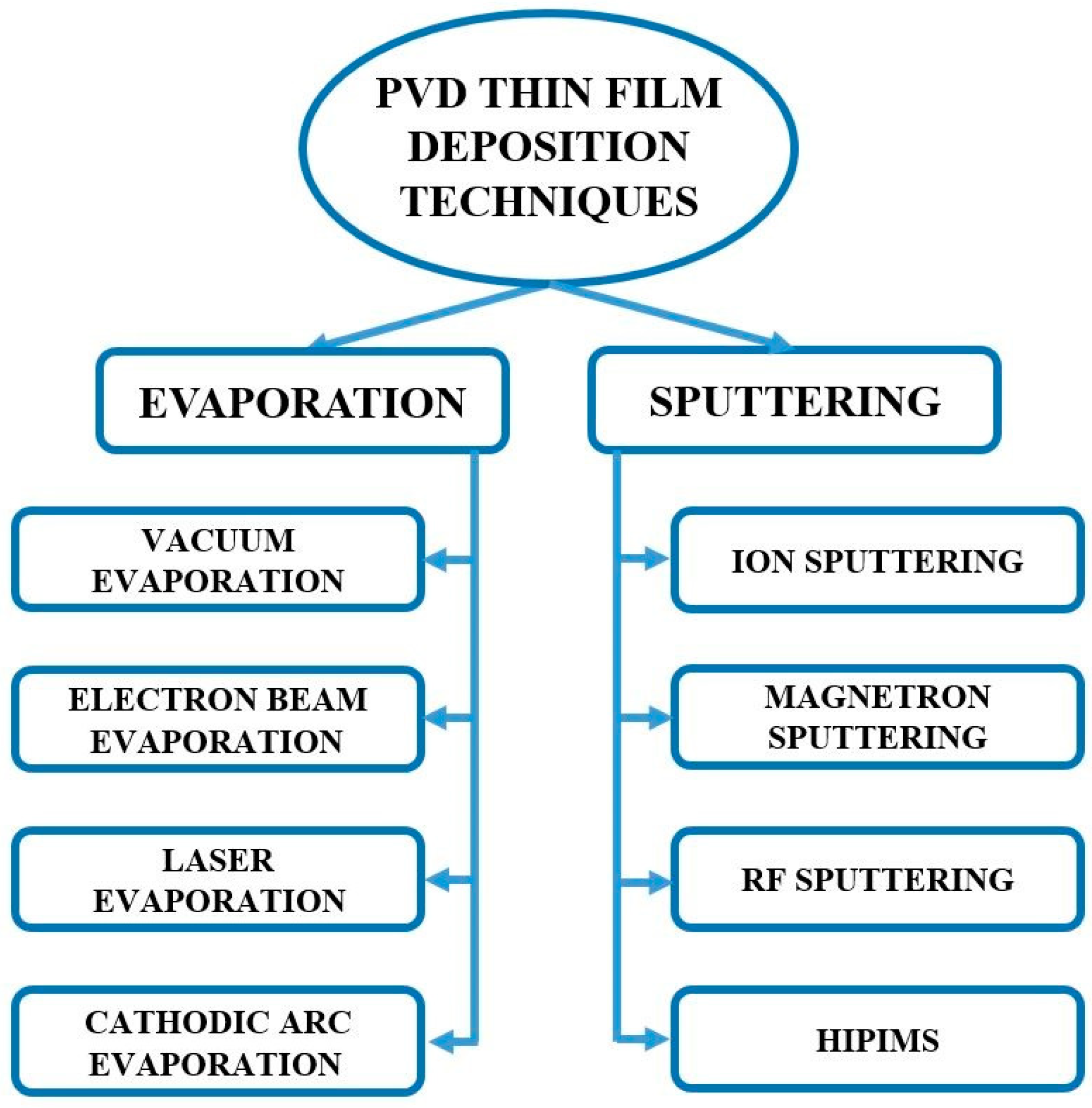
2. PVD Techniques for Thin-Film Deposition

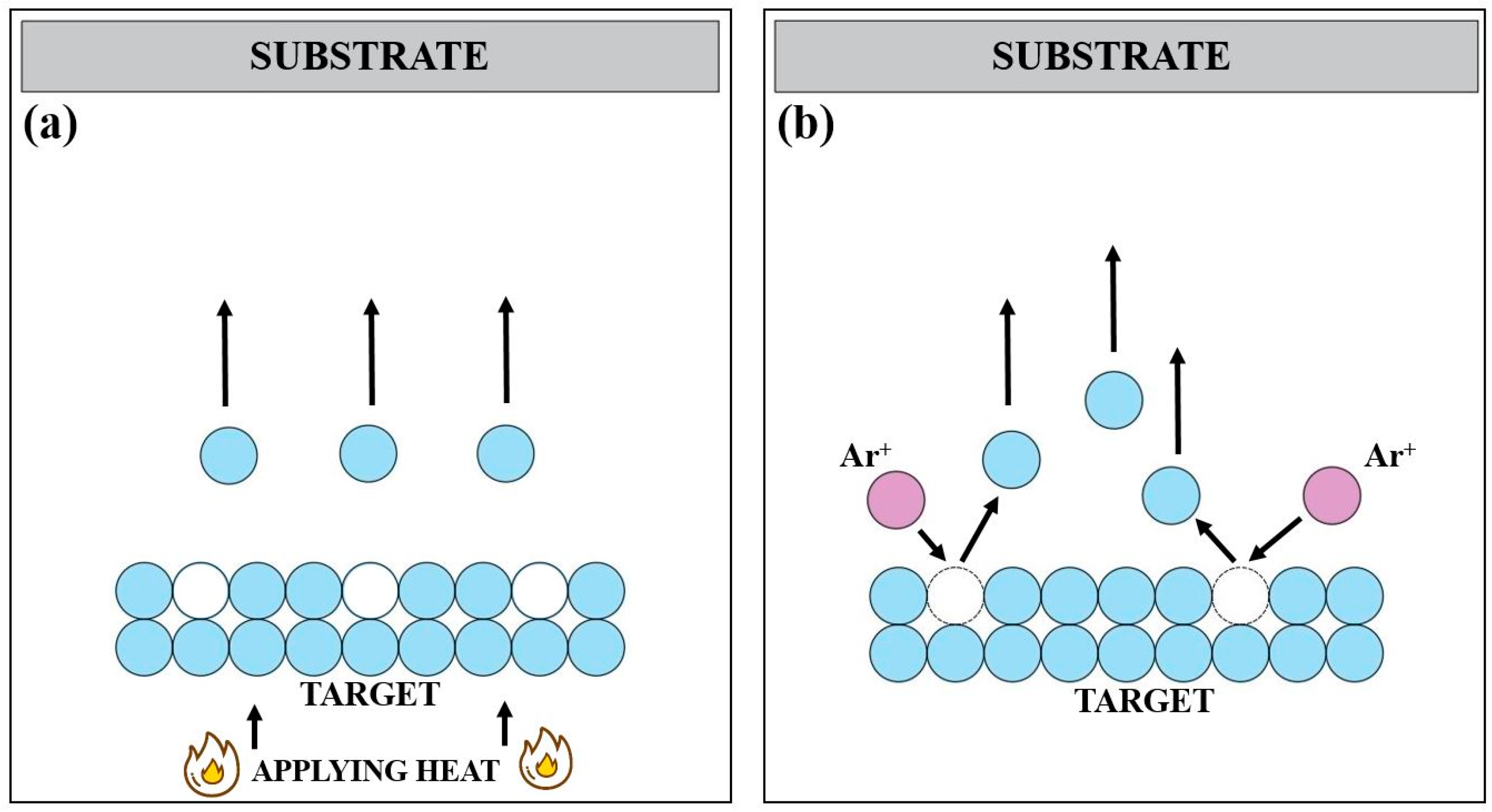
2.1. Fundamentals of Forming Thin Films Using PVD Techniques

The application of thin films atop the surface of substrates can be essentially divided into two categories based on the deposition approach—physical vapor deposition [22] and chemical vapor deposition (CVD) [23]. Physical vapor deposition requires the vaporizing of a solid target, which is followed by the condensation of this material on the surface of the substrate [22]. In contrast a thin film is formed using CVD by vaporizing the target. The formed vapor chemically reacts with the substrate forming a thin layer [23]. In that sense, the deposited material, formed atop the substrates can be categorized either as a thin film or as a coating. Thin films are usually complex and thin (typically form a nanometer to a few micrometers), and are typically used in more complex configurations. Coatings on the other hand are generally thicker (from a micrometer to several micrometers), have a simpler structure, and are mostly used as protective “shells” for the substrates [24]. Due to recent demands for miniaturization of electrical circuits and devices the surface films that will be the focus of the current review are specifically thin films.
The formation of the physical vapor can be performed using different methods with the most common ones being the so-called evaporation (Figure 1a) and sputtering (Figure 1b). The two processes are seemingly highly similar; however, investigating them in detail emphasizes their differences quite well. The vapor in the case of the evaporation processes is typically formed by heating the target until its temperature reaches the temperature of boiling of the material. Heating the material can be performed using resistive or inductive heating, by employing an electron or a laser beams, or even by an electric arc. Natural evaporation processes occur when the target material begins to boil, during which stage particles of the target begin to detach form its surface. The clusters of particles form a vapor mist (or a vapor cloud), which is unidirectional and leading to the substrate. The energized particles condense on the surface of the substrate and form the desired film. Unlike the evaporation process, sputtering relies on generating and utilization of plasma. This is performed by applying a voltage potential between the target (used as a cathode) and the anode (the substrate). An inert gas is introduced in the vacuum chamber. Typically, an inert, low-ionization-energy gas like argon (Ar) is used. The detached electrodes from the cathode collide with the Ar particles and remove an electron from its outer shell. The result of this process is the generation of an Ar+ ion and two free electrons. The process can be formulated as the following reaction: e + Ar → 2e + Ar+. In this case, the application of the correct voltage is crucial for two reasons. Firstly, enough voltage should be applied in order to successfully ionize the gaseous particles and form the plasma. Secondly, if the voltage is too low the plasma will become unstable and can be extinguished, and if the voltage is too high rapid cascade over-ionization could occur, which could lead to transition of the glow discharge into an arc discharge, which could cause damage to the target, substrate, and the overall equipment. The ionized heavy gas particles are naturally attracted to the cathode and collide with its surface, which results in the detachment of particles from the target and the formation of the vapor phase.
The most commonly used evaporation techniques for the formation of thin films, as presented in Figure 2, are as follows: vacuum evaporation, electron and laser beam evaporation, and cathodic arc evaporation. From the sputtering techniques the most commonly applied ones are ion sputtering, magnetron sputtering, RF magnetron sputtering, and high-power impulse magnetron sputtering (HiPIMS).

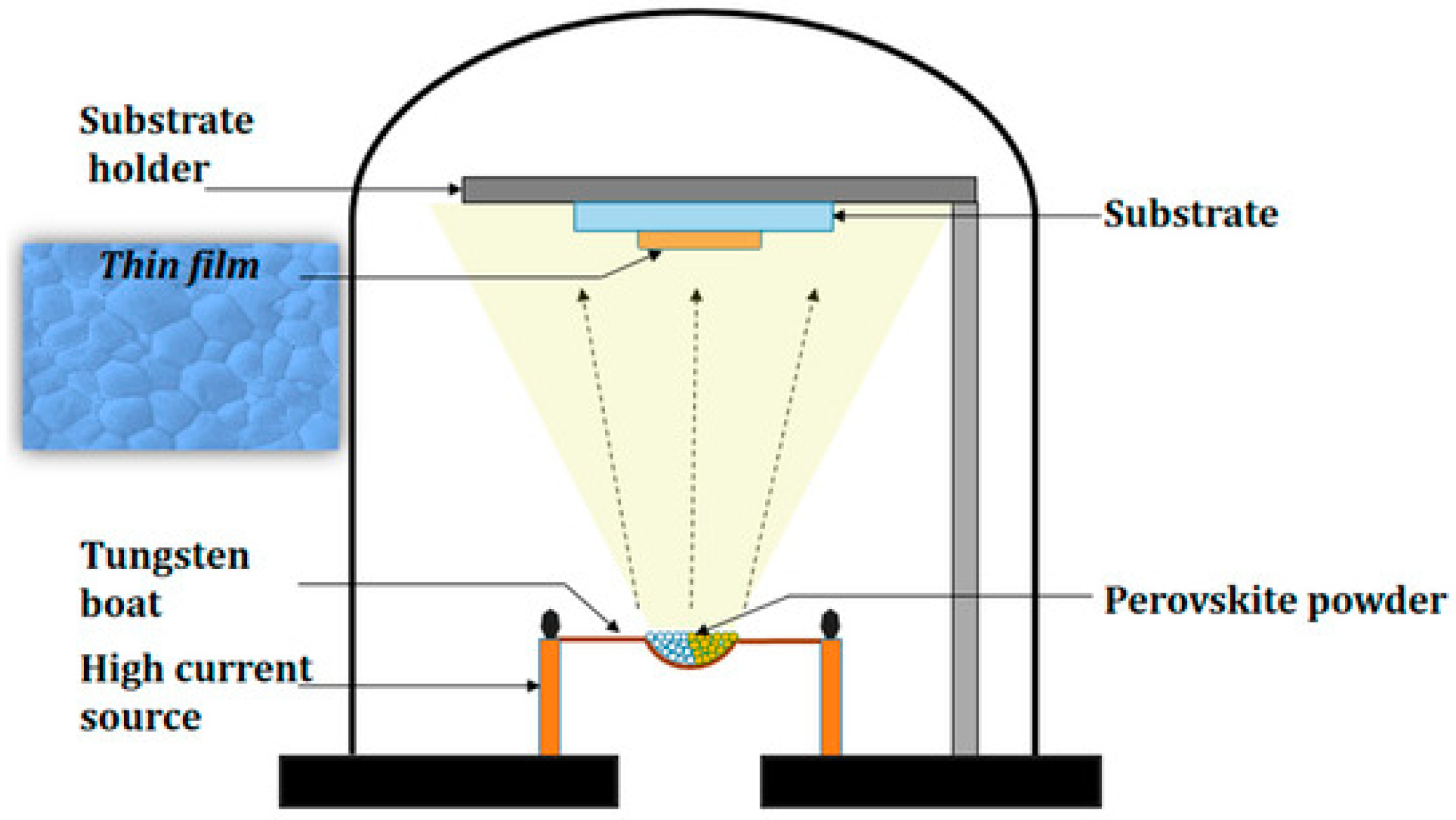
2.2. Vacuum Evaporation

Vacuum evaporation is one of the most basic methods for forming PVD thin films due to its simplicity [26]. Most commonly, a current is passed through a resistive heating source. Due to the heat losses of the material the heat in the heating element increases until it reaches sufficient enough levels to melt the target material. Subsequent to this a detachment of particles occurs. Due to the natural diffusion process, the superheated particles form a vapor mist, the direction of travel of which is directed towards the top of the vacuum chamber. The target particles condense on the surface of the substrate to form the desired film. Typically, tungsten, molybdenum, tantalum, or graphite are used as heating elements due to their high temperature of melting and low reactivity. The target material is often placed directly into the heating element. The disadvantage of this method is the low maximum temperature of the heating element. Due to this only low-melting-temperature materials can be used such as Al, Ag, Au, Cu, Ge, In, Pb, etc. Of course it is possible to evaporate composite materials, as proven by the authors of [26] who formed CsPb (Br0.5Cl0.5)3 perovskite thin films atop glass substrates (Figure 3). An advantage of this method is the possibility of creating high-purity thin films atop polymeric and textile substrates that can be used as conductive medium in modern flexible sensors [27]. For example, the authors of [28] have investigated the applicability of depositing aluminum films atop flexible textile and polymeric materials and have found that doing so ensures excellent electrical properties, even when the substrates are subjected to a high degree of deformation during normal operation.

2.3. Electron Beam-Physical Vapor Deposition (EBPVD)

The second most common physical evaporation technique is electron beam-physical vapor deposition (Figure 4). The authors of [29] have investigated the possibility of using EBPVD to form surface films atop metallic components. The electron beam-physical vapor deposition technique is based on irradiating the target material using an electron beam. The electron beam has to be highly defocused. This way the penetration depth of the electrons is low enough to not form deep craters on the surface of the target. The last is very rapidly heated due to the transfer of the kinetic energy of the electrons into heat. The molten material begins to boil and, similarly to the vacuum evaporation process, particles of it begin to be released in order to form a flow of metallic vapor. The metallic particles condense atop the substrate forming a layer. This method has a number of advantages compared to others such as the high deposition rate, which is higher than the vacuum evaporation one, and significantly higher than that of the sputtering techniques. Another advantage of the EBPVD method is the high thermal input of the electron beam, which allows for the melting and deposition of materials with incredibly high melting temperatures such as carbon, tungsten, molybdenum, and others. Previous research exists, which was focused on the formation of conductive W films atop copper substrates using EBPVD [30]. A drawback of this technique is the low energy of the particles that comprise the vapor, which leads to reduced penetration in the surface of the substrates, and thus lower adhesion. One such way this problem can be improved is by heating the substrate by means of external heating element integrated in the base of the substrate holder [31].

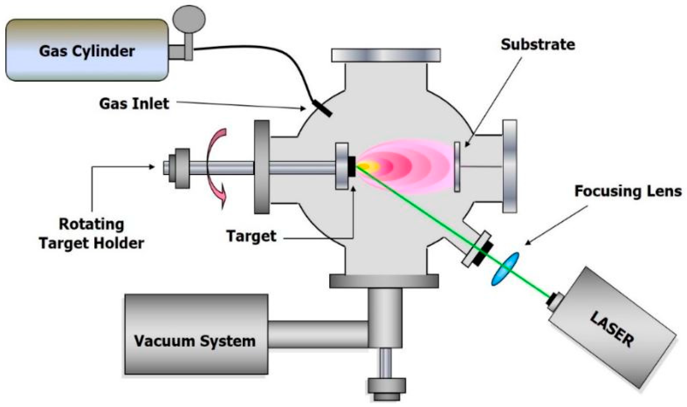
2.4. Pulsed Laser Deposition (PLD)

A similar process to the EBPVD is the laser beam evaporation, more commonly known as pulsed laser deposition—PLD [32]. The process, as shown in Figure 5, is carried out in a vacuum environment as in the previous cases, which guarantees the purity of the films, at least when the influence of outside particles is concerned. In this case the substrate is irradiated with a laser beam, as a result of which a plasma flow consisting of target material particles is formed. The thin film forms by condensing on the surface of the substrates. The laser beam also has a very high thermal input, along with extremely high precision, which makes it ideal for the deposition of non-refractory metals and also the formation of nano-structured thin films [33,34,35]. A new and innovative approach to PLD is the so-called Matrix-Assisted Pulsed Laser Evaporation (MAPLE), which can be used to form surface films atop metallic, polymeric, and even highly sensitive organic materials. This method is highly regarded also due to the formation of films with better properties such as specific crystallinity, high purity, and preserved chemical structure, which significantly improves bio-compatibility, and more [36].

2.5. Cathodic Arc Evaporation

Cathodic arc evaporation is another evaporation technique commonly used for the deposition of thin films. An exemplary schematic of the process is shown in Figure 6 [38]. An electric arc is ignited either mechanically with an additional ignition electrode or electrically by a high-voltage impulse. The electric arc forms a self-sustainable arc plasma channel, which continuously burns and evaporates the cathode material. The arc discharge is characterized by low voltage and high current. The current densities reached by the electric arc, depending on the applied setup, are in the range of 105 A/m2 to 1011 A/m2 [39]. The formed particle vapor is directed using magnetic coils to the substrate. One of the most important technological conditions for the successful deposition of thin films using cathodic arc evaporation are the temperature of the substrate and the applied negative bias voltage [39]. This technique allows for the deposition of both pure metals such as Ti, Al, Cr, Zr, and others, as well as alloys and ceramics such as TiAl, CrAl, ZrN, TiN, MoN, CrN, and more [39,40,41,42,43].
Based on the obtained data Table 1 was formed, that includes a total summary of the advantages and disadvantages of the different evaporation techniques, namely vacuum evaporation, electron beam-physical vapor deposition, pulsed laser disposition, and cathodic arc evaporation.

2.6. Ion Sputtering

Figure 7 depicts a simplified scheme of the ion sputtering process. This is the most basic and fundamental sputtering process due to its simplicity. The process of applying a thin film using this method was already described above. A DC voltage potential is applied between the cathode and the anode placed in a vacuum chamber in a high-vacuum environment. This is crucial for the realization of the process. An inert gas, commonly Ar, is introduced in the vacuum chamber and ionized. The heavy gas ions bombard the target and detach particles from it. The last then condense on the substrate and form a layer atop its surface. The particles have a much higher energy compared to the ones formed using the evaporation methods, which means higher penetration in the surface of the substrate. This not only improves adhesion significantly, increases the density of the films, but also results in the formation of a smoother surface of the formed layer. The integration of the vaporized particles in the surface of the substrate can be further improved by heating the working table [44]. The advantages of the ion sputtering method are good control of the ion generation process, good uniformity of the films, and low target heating. The main disadvantages are related to a number of factors. The plasma efficiency of this method is low, resulting in lower deposition rates. Additionally, very precise control of the ionization process is needed, since in this case the energy of the ions is so high it is borderline at the edge of an arc discharge. Even small inconsistencies of the plasma flow could lead to an arc discharge.

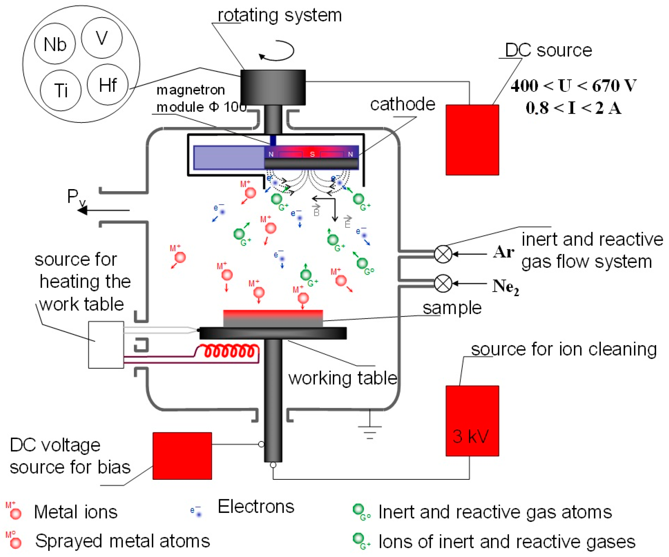
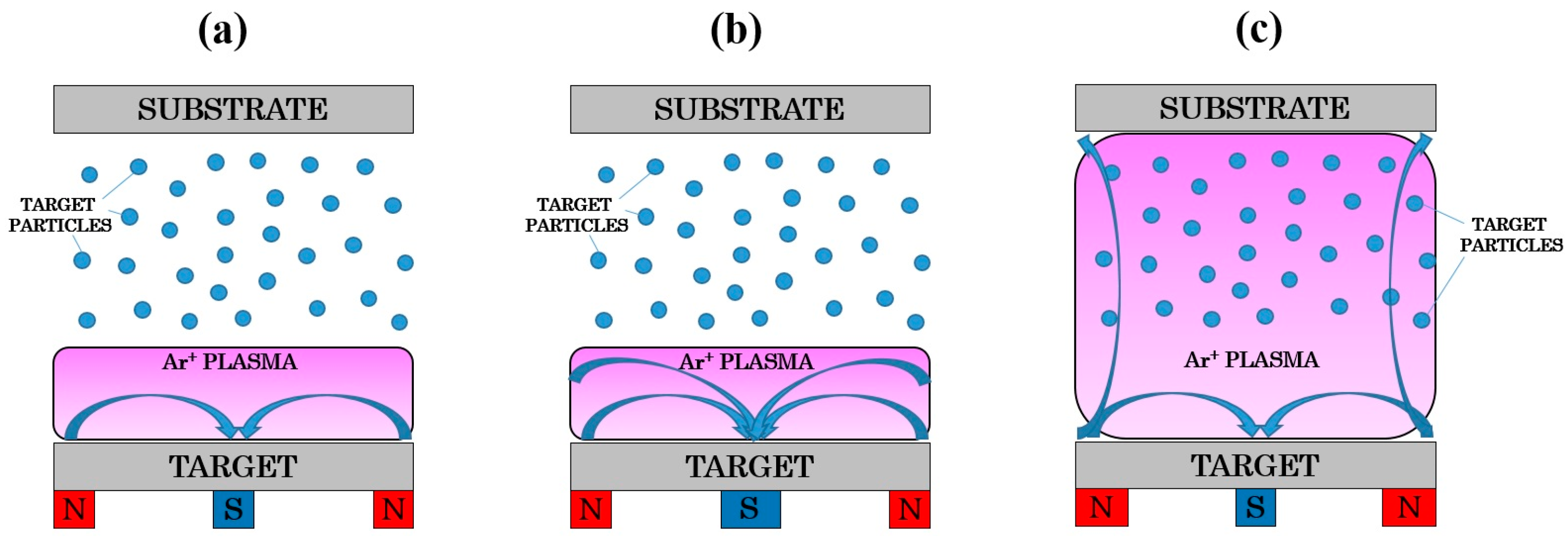
2.7. Magnetron Sputtering

Magnetron sputtering is one of the most common and widely used methods for the deposition of thin films. It is based on the operational principle of the ion sputtering process. In this case, however, magnets are positioned immediately under the target. An exemplary schematic of a DC magnetron sputtering unit with a balanced magnetron is shown in Figure 8. The magnetron is considered balanced due to the closed magnetic field. The generated magnetic field results in a major improvement of the plasma efficiency. The magnetic flux not only traps the electrons close to the target, but changes their direction of movement. Instead of quickly passing over the target, they begin to spiral, which also improves the ionization efficiency of the electrons. Due to this the ionization process can take place by applying a lower voltage of the power source. The main advantages of the magnetron sputtering technique are the higher deposition rates compared to ion sputtering, which is a process with higher efficiency, and then since the ions have less energy the possibility of damaging the substrate is lower. The higher rate of ionization (sputtering) can lead to increased heat at the target, which imposes the necessity of active cooling of the magnetron. Another disadvantage is that although compared to the ion sputtering process, the plasma efficiency is substantially improved, it is still quite low for the purposes of thin-film deposition, since the plasma flow preferentially remains in a closed field next to the target. A low amount of ions and electrons reach the substrate. As a result of this, the deposition rate is low, and the structure of the final film could be affected as well, considering factors such as thickness, adhesion, crystal properties, internal stresses, etc.
In order to overcome this issue, typically, an unbalanced magnetron configuration is applied. The “unbalancing” of the magnetron is carried out by either increasing the strength of the outer magnets of the electron compared to the center magnets, or by increasing the strength of the central magnets. The resultant plasma flow is different depending on the preferred method, as shown in Figure 9 [13]; however, in all cases this configuration allows for more ions and electrons to flow to the substrate. As a result, the obtained thin films have better uniformity, higher adhesion, lower surface roughness, improved crystals structures, and more, over ones deposited using a balanced magnetron sputtering configuration. The disadvantages of the unbalanced magnetron sputtering, however, are of a higher substrate temperature due to the increased interaction of the ions with it, faster wear of the target, and higher interaction of the ions with the walls of the vacuum chamber, leading to increased contamination.
Reactive DC magnetron sputtering can be performed with either configuration of the magnetron (Figure 10). It is achieved by introducing a reactive gas into the vacuum chamber during the deposition process (typically oxygen or nitrogen) in order to achieve TMO or TMN, respectively. The active gas molecules react with the metal particles and form metal-nitride or metal-oxide compounds. It is possible that the reaction occurs at the surface of the substrate. Contamination of the target is also possible. Due to this, special precautions are required when using this method. One of the most important factors when considering this deposition technique is the careful selection of the proportion of inert gas/active gas. This not only directly affects the stoichiometry of the obtained films, but increasing the inert gas flow could disrupt the reaction between the active gas and the vaporized particles. On the other hand, increasing the active gas flow beyond certain levels could lead to the mentioned contamination of the target. The careful selection of the technological conditions during magnetron sputtering is of upmost importance for the formation of thin films with optimal structure and applications. The ratio of the inert gas/active gas flow can also result in the formation of different crystal phases, some of which may be undesirable in the particular case. The deposition temperature is also highly important for a successful deposition process, since it not only is necessary, particularly when materials with significantly different thermophysical properties are used, but it also can be used for modulating the resultant structure of the layers such as the microstructure [46,47], phase composition [48], crystallographic orientation of the particles [49], internal stresses [50], etc. The last, of course, influences their potential applications as well.

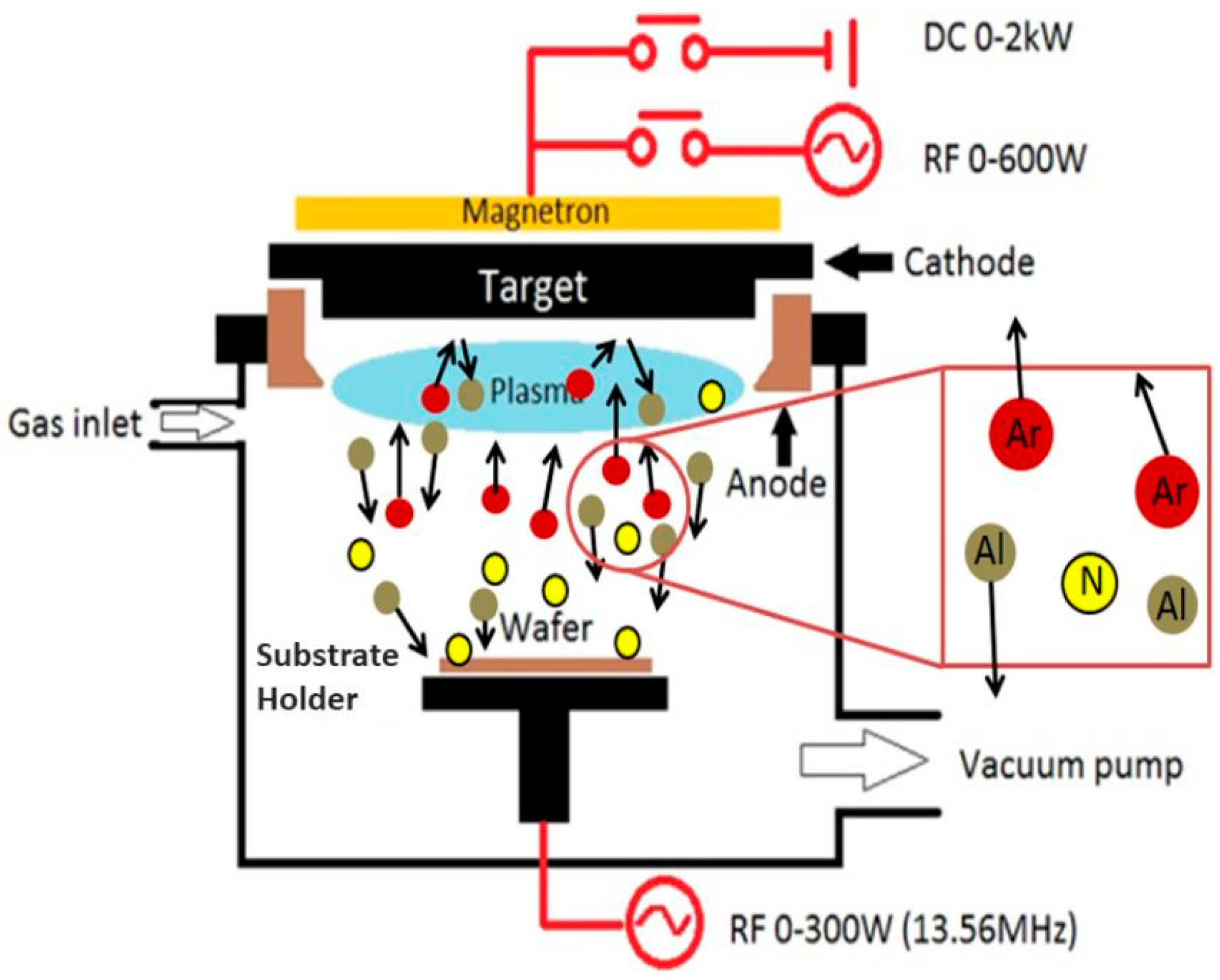
2.8. Radio-Frequency (RF) Magnetron Sputtering

One of the biggest disadvantages of the DC magnetron sputtering technique is the limitation in the deposition of polymeric materials. Furthermore, in some instances adhesion of the layer is problematic, so another method was developed for further improving the quality of the formed thin films, employing the application of an AC radio frequency input power source, typically with a frequency of 13.56 MHz [51], as shown in Figure 10. The application of an AC power supply results in a repetitive reversing of the polarity of the electrodes, which negatively influences the plasma flow. However, it is precisely due to the variable polarity that it is possible to deposit polymers, since it prevents the build-up of charges atop the surface of the both the target and the substrate. The main advantages of the RF magnetron sputtering are the formation of denser films with smoother surfaces [52], lower internal stresses [53], improved adhesion [54], and better controllability [55]. Of course the main advantage is the possibility to deposit polymeric films [56]. The main disadvantage of such a system is the reduced deposition rate due to the reduced efficiency of the plasma [57].

2.9. High-Power Impulse Magnetron Sputtering (HiPIMS)

High-power impulse magnetron sputtering (HiPIMS) is a variation in the magnetron sputtering technique introduced by Kouznetsov et al. [58]. Conventional DC magnetron sputtering, as mentioned above, has one major disadvantage, and that is the low ionization of the sputtered particles and the low efficiency of the plasma. To overcome this issue HiPIMS introduces the application of high-powered impulses with high power densities in the range of 1–10 kW/cm2 [59]. High frequency of the pulses is usually employed in order to avoid excessive heating and damage to the target. Due to the high power of the impulses, more of the sputtered particles are ionized, which results in the formation of a denser plasma [60]. The charged particles more successfully reach the substrate in this regime, which results in the formation of films with higher density, adhesion, purity, and more. Due to the high level of ionization of the particles, a high degree of controllability of the deposition process is possible, which allows for the formation of highly specific layers with unique structures and properties [61]. Another advantage of this method is that a standard magnetron could be used to deposit the films by retrofitting it with a new power supply that enables this work mode. The only disadvantage of this method compared to other sputtering deposition techniques is the low deposition rate, due to the high degree of ionization of the particles. Using this technique, it is possible to deposit a number of materials including metals [62], alloys [63], ceramics [64], and polymers [65].
Based on the obtained data, Table 2 was formed, which includes a total summary of the advantages and disadvantages of the different sputtering techniques, namely ion sputtering, direct current (DC) magnetron sputtering, radio-frequency (RF) magnetron sputtering, and high-power impulse magnetron sputtering (HiPIMS).

2.10. Summary of Sputtering Techniques

In this section different PVD techniques were presented and their advantages and disadvantages were described. It is important to mention that some of the studied methods were of the most basic kind and new and improved methods arise constantly. However, these methods are still highly valuable, well established, and used in practice. Due to this it was mandatory to include them in the presented expose. Based on them thin films of simplistic (single layer) and complex (multi-layer) structures alike can be formed. Highly popular films are based on the transition metal-oxide (TMO) and transition metal-nitride (TMN) compounds. They can be used in a vast array of applications both scientific and industrial. Due to the particular interest of the last towards TMO and TMN thin films their properties and applications will be investigated in Section 3 and Section 4 of this article.

3. Formation of Metal-Oxide Thin Films and Their Applications

The formation of metal-oxide thin films is usually based on the introduction of some amount of oxygen along with the argon gas, where the Ar/O2 ratio is very important. The formation of metal-oxide thin films is a critical process in a wide range of industrial and technological applications. These films, formed on the surfaces of metals, serve many functions, such as, enhancing surface properties from a biomedical point of view, or enabling advanced functionalities like conductivity, catalysis, photocatalytic properties, etc. As already mentioned, the formation of oxide films is based on the introduction of oxygen gas in the vacuum chamber (or most commonly, a mixture of argon and oxygen), which allows the formation of the O-based structure.
Metal-oxide thin films can be deposited through various techniques where the physical vapor deposition (PVD) is the most commonly used [66,67,68]. These methods allow for precise control over the film’s thickness, composition, and structure. The properties of metal-oxide thin films can be easily tuned by modifying parameters [69]. This flexibility allows for the optimization of properties for specific applications. Thin films can be created at relatively low temperatures, making them compatible with flexible substrates and facilitating their use in flexible electronics [70,71].
Nowadays, metal-oxide thin films are interesting because of their unique properties and wide range of applications [67,72]. Many metal oxides are semiconductors, making them useful in devices like sensors [72,73,74,75], solar cells [76,77], and photodetectors [78]. Their electrical properties can be tuned by adjusting factors like film thickness, and doping. Metal-oxide films are used in electronics, such as transistors, sensors, capacitors, and thin-film transistors (TFTs) [79,80,81].
The authors of [82] manufactured porous nanocrystalline WO3 thin films using ion beam sputtering. They discovered that this technique enables the production of porous WO3 layers with distinctive optical and electrical properties, making them highly suitable for applications in photoelectric devices and thermistors. The same authors concluded that these attractive functional properties of the WO3 films are attributed to their porosity. Similarly, in study [83] fluorine-doped tin oxide (SnO2/F) thin films were successfully deposited on glass substrates via pulsed DC magnetron sputtering. Among the various doping levels investigated, a fluorine concentration of 5.3 at.% yielded the most favorable electrical properties. This enhancement is primarily attributed to improved film crystallinity induced by optimal fluorine incorporation. Electrical characterization revealed that at this doping level, the film exhibited a minimum resistivity of 6.71 × 10⁻³ Ω·cm.
Metal-oxide thin films are employed in optical devices like mirrors, lenses, and as antireflective surfaces due to their ability to reflect or absorb light of different wavelengths [84,85,86]. The authors of [86] have studied the influence of deposition time of HfO2 films applied on glass substrates on the surface roughness and optical properties. The results obtained by the authors of [86] showed that the roughness of the surface and refractive index remain almost independent from the time of deposition. However, the extinction coefficient is higher in the case of higher deposition time. Also, the same authors mentioned that the films are smooth, uniform, and dense, which make them very suitable for optical elements.
On the other hand, metal oxides are often used as catalysts or in catalytic converters, which play a significant role in environmental protection by breaking down pollutants [87,88]. Some metal oxides, such as titanium dioxide (TiO2), exhibit photocatalytic properties, meaning they can use light energy to drive chemical reactions. This is useful for environmental cleanup and energy applications [87]. The authors of [89] deposited patterned TiO2 films on glass substrates using different pattern masks, as well as non-patterned films. The photocatalytic activity of the thin films was evaluated under UV irradiation using three model degradation assays: methylene blue, stearic acid, and oleic acid. All micro-patterned films exhibited enhanced photocatalytic performance compared to non-patterned TiO2, with the improvement being particularly significant in the stearic and oleic acid degradation tests. This pronounced effect is likely attributed to the direct contact between the photocatalyst surface and the organic pollutants in these solid-phase assays, which facilitates more efficient degradation.
Metal-oxide films can provide excellent protection against corrosion, making them ideal for use in harsh environments (e.g., marine or industrial applications) [90,91]. Some metal oxides are biocompatible, making them suitable for medical devices and implants [92,93,94]. Ilievska et al. [95] studied the influence of thickness of Cu-O-based thin films on the antibacterial response deposited by reactive magnetron sputtering. The results obtained by the authors showed that with an increase in the thickness, the antibacterial and corrosion activities were greatly improved. Similarly, the investigations carried out by M. Nikolova et al. [92] studied the effect of co-sputtered copper and titanium oxide thin films on bacterial resistance and cytocompatibility of osteoblast cells. The films were deposited at different negative bias voltages applied to the substrate. The voltage was in the range from 0 to 100 V, namely 0 V, 50 V, and 100 V. The results indicated that the −50 V biased Cu-doped TiO2 thin films exhibited favorable biocompatibility, supporting cell spreading while maintaining effective antibacterial activity. In contrast, the non-biased films, characterized by higher ion release and greater surface hydrophilicity, induced altered osteoblastic cell morphology and demonstrated superior antibacterial performance. These results highlight the capability of reactive co-sputtering to finely tune the copper content and phase composition within the TiO2 matrix, enabling controlled biological behavior in vitro. Overall, the Cu-doped TiO2 thin films proved to be biocompatible, non-cytotoxic, and exhibited enhanced antimicrobial activity—demonstrating strong potential as safe and efficient surface films for biomedical applications, particularly in addressing infection-related challenges.
Meanwhile, some metal oxides are also used in green energy technologies where their properties contribute to improving energy efficiency [96,97]. Table 3 presents data of some oxide-based films formed via different PVD methods, as well as their functional properties and potential applications.
Overall, metal-oxide thin films combine high functionality, versatility, and unique material properties, making them indispensable across a variety of industries. Their ability to be engineered for specific applications and their potential for innovation in emerging fields contribute to their continued importance. However, most of these works are based on the deposition of advanced oxide-based films by other deposition techniques. The articles of the deposition and characterization of oxide surface structures for the purposes of the modern electrical engineering formed by the methods of PVD are still very limited within the worldwide scientific literature. Therefore, from the point of view of the authors, more attention should be paid to the structure formation and its influence on the important electrical properties of oxide-based films deposited by PVD methods.

4. Formation of Nitride Thin Films and Their Applications

The deposition of nitride-based ones is usually based on the introduction of some amount of nitrogen along with the argon gas, where the Ar/N2 ratio is very important. Nitrides are compounds that consist of nitrogen combined with a metal or metalloid. Nitride thin films are typically formed by methods that allow nitrogen to react with metal surfaces or vaporize metal precursors to form a thin layer of nitride material. These films are commonly used for improving surface properties like hardness, wear resistance, and corrosion resistance. Like the oxide-based thin films, the formation of nitride films is based on the introduction of nitrogen gas in the vacuum chamber (or most commonly mixture of argon and nitrogen), which allows the formation of the N-based structure.
Similarly to oxide-based films, the nitride-based thin films are most commonly deposited by PVD methods [99,100,101]. The functional properties of nitride thin films can be easily modified by variable parameters like time of deposition, different deposition method, and post-deposition treatments [67]. This allows for the optimization of properties for specific applications.
Metal-nitride films are widely used in various industrial applications due to their enhanced hardness, wear resistance, corrosion resistance, electrical conductivity, and thermal stability [102,103,104]. These films are crucial in numerous industries, from mechanical tools to electronics, where their unique characteristics can significantly improve device performance and durability [105,106]. As mentioned previously, the TMO films are used mostly for biomedical, optical, and photocatalytic purposes, which makes them applicable in different practical and industrial fields. The most attractive TMN properties are described below in order to highlight the most relevant practical applications of these films.
TiN and CrN are commonly used as hard films for cutting tools, drill bits, and molds [107]. These films increase wear resistance and enhance cutting performance by reducing friction and heat during machining processes. Also they can enhance the hardness and durability of materials, which is beneficial for improving the lifetime of tools and components [108]. At the same time, TiN and other metal-nitride films exhibit low friction coefficient, which make them ideal for reducing wear in sliding or contact applications, such as in mechanical components and cutting tools [109]. On the other hand, metal-nitride thin films, such as AlN and TiN, exhibit excellent thermal stability. These films can withstand high temperatures without degrading, making them ideal for aerospace, automotive, and high-temperature industrial applications [110,111].
Nitride thin films, particularly TiN and ZrN, are used in medical devices like prosthetics, and surgical tools because of their resistance to corrosion, and enhanced mechanical properties [112,113]. Considering TMN, it was demonstrated that, in addition to oxide-based structures (described in Section 3), the TMN films can be used for antibacterial purposes. The authors of [114] have studied the antibacterial properties of composite CrN/Ag, ZrN/Ag, TiN/Ag, and TiN/Cu films deposited by pulsed magnetron sputtering. and their results showed that the copper-doped titanium nitride films exhibited the most active antibacterial properties where this effect is more pronounced with an increase in the copper content. Therefore, it could be concluded that both nitride and oxide films have antibacterial properties when some amount of elements with antibacterial properties were added. These statements point out that independent to the nature of the film (e.g., nitride or oxide), the antibacterial characteristics can be successfully controlled. Following these results, some similarities between TMN and TMO in terms of antibacterial properties could be mentioned.
Many nitrides like TiN, CrN, and AlN are resistant to oxidation and corrosion, extending the lifespan of components exposed to harsh environments, such as high temperatures or corrosive elements [115,116]. At the same time, they maintain their properties at elevated temperatures, making them suitable for high-temperature electrical applications. Most metal-nitride thin films (TiN, CrN, AlN, etc.) form a stable and dense oxide layer when exposed to air at elevated temperatures, protecting the underlying material from further oxidation [117]. This oxide layer acts as a barrier, preventing the metal from deteriorating due to environmental exposure. Nitride films generally have low oxygen diffusion rates, meaning oxygen has difficulty penetrating them and reacting with the base material underneath [118]. As mentioned in the previous chapter, similar properties were attributed also to the oxide-based films, meaning that they can be successfully applied in the fields where high corrosion-resistance is needed.
In the global scientific literature, data is present regarding the utilization of transition metal-nitride thin films in the process of photocatalysis for water splitting, organic dye degradation, and CO2 reduction [119,120]. For example, nitride-based films (Ta3N5, InGaN, etc.) were used as semiconductor photocatalysts for water splitting due to their simple chemical composition, tunable narrow band gap, and stability [121,122,123].
Some nitrides, like titanium nitride, can be conductive, while others, such as silicon nitride (Si3N4), can act as electrical insulators, depending on the specific material and structure. Another typical representative of nitride thin films is AlN, which is widely used in high-power electronics for heat dissipation [124,125]. Its exceptional thermal conductivity (about 200–280 W/m·K) makes it an ideal material for heat sinks and substrates for power devices, such as power transistors, diodes, and LEDs, which generate a lot of heat during operation [126]. AlN is used in microwave and RF (radio frequency) components, where its low dielectric loss and high thermal conductivity are beneficial. It is often used in the creation of substrates for RF and microwave devices like amplifiers and filters [127,128].
Some metal-nitride films can be used for electromagnetic interference (EMI) shielding to protect sensitive electrical components from external electromagnetic interference [129]. The researchers in [130] successfully deposited titanium-nitride (TiN) films using reactive magnetron sputtering, varying the sputtering power from 30 to 250 W. The study highlights the significant impact of this parameter on the structure and properties of the TiN thin films. It was observed that as the sputtering power increased, the roughness of the titanium-nitride films also increased, resulting in enhanced super-hydrophobicity. Furthermore, the electromagnetic shielding effectiveness of the TiN films was significantly improved at 250 W, reaching approximately 40 dB. This enhancement was attributed to a combination of factors: reduced electrical resistivity, greater film thickness, and a unique topography of the thin films. These findings suggest that TiN films deposited at higher sputtering powers are promising candidates for industrial applications requiring electromagnetic shielding [130].
TiN and CrN are often applied to electrical conductors to improve their conductivity and reduce the formation of contact resistance over time [131].
Most transition metal nitrides (e.g., TiN, ZrN, VN, WN, TaN) are considered stable electrode materials for supercapacitors due to their affordability, exceptional electrical conductivity, high thermal stability, and strong resistance to chemical degradation [132,133,134]. Some nitride-based films exhibit excellent characteristics, such as high specific capacitance, exceptional chemical and thermal stability, and excellent electrical conductivity, making them suitable for applications in lithium-ion batteries and capacitors. Notable metal nitrides, including TiN, VN, FeN, and CrN, are emerging as promising electrode materials for energy storage devices [135,136]. In the production of thin-film solar cells, certain metal nitrides can be used to enhance performance and energy conversion efficiency [137].
In Refs. [138,139], the authors investigated the electrochemical behavior of vanadium-nitride (VN) thin films prepared by direct-current reactive magnetron sputtering. They studied the influence of film thickness on electrochemical performance, particularly focusing on the specific capacitance. VN films with a thickness of 25 nm exhibited the highest specific capacitance of 422 F·g−1. Also, the active volume of the films remained consistent across different thicknesses, indicating that film thickness did not significantly impact the active volume involved in electrochemical reactions. Furthermore, VN films with a thickness below 100 nm achieved a volumetric power density of 125 W·cm−3—comparable to that of electrolytic capacitors—while offering a significantly higher volumetric energy density of 0.01 Wh.cm−3. This demonstrates the potential of combining high capacitance with excellent electronic conductivity, making VN films promising candidates for advanced energy storage applications such as supercapacitors.
The authors in Ref. [140] demonstrate the possibility of the formation of a highly efficient supercapacitor electrode, including a tungsten-nitride (W2N) thin film deposited on a stainless steel substrate using reactive magnetron sputtering. The study shows that the W2N thin film exhibits a high specific capacitance of 163 F·g−1 at 0.5 mA·cm−2, coupled with excellent cycling stability. The symmetric supercapacitor device achieves a high specific capacitance of 80 F·g−1, with remarkable longevity, maintaining 90.46% of its capacitance after 10,000 cycles. Additionally, it delivers a high energy density of 12.92 Wh·kg−1 and power density of approximately 674 kW·kg−1 at 9.36 Wh·kg−1. These outstanding electrochemical performances suggest that the W2N thin film-based supercapacitor is a promising candidate for energy storage applications.
Reference [141] explores the preparation of nanostructured porous CrN thin films using oblique angle magnetron sputtering and their application in supercapacitors. The resulting thin film electrode exhibits a high specific capacitance of 17.7 mF·cm−2 at a current density of 1.0 mA·cm−2. Additionally, the symmetric supercapacitor device based on the CrN film achieves maximum energy and power densities of 7.4 mWh·cm−3 and 18.2 W·cm−3, respectively. It also demonstrates excellent cycling stability, retaining 92.2% of its capacitance after 20,000 cycles at a current density of 2.0 mA·cm−2. The oblique angle magnetron sputtering technique proves to be a modern method for manufactured nanostructured porous nitride-based films, offering promising potential for electrochemical energy storage and conversion applications.
The researchers in ref. [142] investigated the impact of working pressure of the electrochemical properties on porous TiN electrode films deposited via reactive magnetron sputtering. The results demonstrate that increasing the working pressure leads to an increase in their porosity and a greater presence TiOxNy fractions, which in turn enhances the real capacitance (ranging from 0.3 to 4.7 mFcm−2). Furthermore, the fabricated solid-state supercapacitors achieved excellent energy and power densities of 23 mWh cm−3 and 7.4 W cm−3, respectively. After 10,000 cycles of continuous charge/discharge, the device showed outstanding durability with negligible capacitance decay. The superior energy storage, power densities, and long-term stability make these electrodes ideal candidates for high performance on-chip supercapacitors.
Following the data presented above, it is clear that the TMN films can be successfully incorporated into a number of practical needs where improved electrical properties are required. The same can be said about the TMO surface formations. However, a detailed comparison of the aforementioned properties between both types of films is still missing, or this topic is not very well investigated. Therefore, further research can be conducted for the evaluation of these characteristics, which are very important for the industry, of the discussed films which are expected to clarify the important questions related to the specific electric and electromagnetic applications of the films. Table 4 presents data of some nitride-based films formed via different PVD methods, as well as their functional properties and potential applications.
The formation of nitride thin films involves sophisticated techniques that allow for the customization of materials with enhanced mechanical, electrical, and thermal properties. Their applications across industries like manufacturing, electronics, aerospace, and healthcare continue to grow due to their ability to improve the performance and longevity of products. It is very important to note that the aforementioned superior properties of nitride-based films are strongly related to their structure. Due to that, there exist some articles based on the detailed investigation of the crystallographic structure as a function of the applied technological conditions during the film’s deposition. Iordanova et al. [151] studied the effects of thickness on the important crystallographic parameters and surface topography of TiN films deposited by DC and pulsed reactive magnetron sputtering. Their results showed that the increase in the thickness of the films leads to a change in the preferred crystallographic orientation, where in the case of pulsed mode, this effect is much more pronounced. It was found that at a thickness of 50 nm, the films are oriented towards the {111} family of crystallographic planes with a contribution of 100% in both considered cases. The increase in the thickness to 500 nm tends to result in the transformation in the preferred crystallographic orientation where the contribution of the {111} family of crystallographic planes becomes weaker. This effect is more pronounced in the case of the deposition of TiN films in pulsed mode. These findings are very important from a practical applications point-of-view, since the orientation of the micro-volumes strongly influences the functional properties of the films. According to the authors of [151,152], these structural characteristics can be controlled very precisely by controlling the process parameters of the film’s deposition.

5. Comparison Between the Properties and Applications of TMO and TMN

The literature review in Section 3 and Section 4 evaluates the functional properties and potential practical applications of different transition metal-oxide and transition metal-nitride films deposited by PVD techniques. These data are summarized in Table 3 and Table 4. It is clear that both kinds of thin films and layers have a wide range of potential practical applications, and therefore, they deserve to be distinguished as multifunctional materials, since they can be applied in the fields of modern automotive, aircraft industries, implant manufacturing, and other modern fields of application. However, following the data presented in the aforementioned tables, it is obvious that both types of films can be applied in different fields of application. For example, oxide-based films can be potentially applied in the fields of optical instruments, photovoltaic devices, films for the needs of the modern biomedicine, self-cleaning surfaces, and photoelectrochemical devices. On the other hand, nitrides can be used mostly for protective purposes, where high hardness, wear, and corrosion resistance are required. This means that the TMO and TMN films can be used in different industrial branches, which limits the range of their applications. However, there exist some particular cases where the combination of both types of functional characteristics is required. For example, some materials which are developed for the needs of modern biomedicine could serve in aggressive environments, and in addition to enhanced biocompatibility, improved wear and corrosion resistance is required. A typical example of this kind of requirement is the fabrication of implants and implant manufacturing. Also, materials for modern dental medicine should also be considered as an example. Also, the formation of self-cleaning and photocatalytic surfaces has to possess these requirements. The same can be said about the films developed for lenses and other optical elements. All these examples demonstrate the requirements for the combination of both types of films (i.e., TMO and TMN). Therefore, solutions related to the combination of the properties and practical performance of oxide- and nitride-based films should be pointed out. In this sense, the following chapter is concentrated on the evaluation of the possibilities of the formation of oxy-nitride thin films.

6. Formation of Oxy-Nitride Thin Films and Their Applications

The combination of oxides and nitrides in the form of thin films (i.e., formation of oxy-nitride-based films) is currently not very well studied. Nevertheless, there exist some investigations concerning the formation of such thin films by the deposition of multilayer TiN/TiO2 structures. The authors of [153] studied the possibility of formation of multilayer TiN/TiO2 films on Ti5Al4V alloy via DC reactive magnetron sputtering, where the substrate was preliminarily subjected to a modification by a scanning electron beam. Their results showed that this dual modification of the titanium alloy led to reduced coefficient of friction and wear resistance, reduced Young’s modulus, and, at the same time, small increase in the surface roughness, corresponding to higher surface area. The authors claimed that this modification is of major importance for the application of the alloy for biomedical applications since the extended surface area supports the cell adhesion. Moreover, the decreased modulus of elasticity is much closer to that of human bones which is very important for the implant materials. These changes in the functional characteristics are attributed to the observed structural transformations of the deposited films. Similar investigations were conducted by the authors of [49], where the Co-Cr-based alloy was covered by a bilayer TiN/TiO2 film, where the influence of the preliminary treatment of the substrate was studied. The results again reveal that the treatment procedure led to a small increase in the surface roughness, and therefore, surface area, and a decrease in the friction coefficient. The change in the functional characteristics is attributed mostly to the transformation into the preferred crystallographic orientation. This again is expected to have some practical applications in the field of the modern biomedicine.
However, studies based on the formation of another type of oxy-nitrides (except titanium-based structures) are still less well studied. Therefore, additional investigations should be performed on another type of oxy-nitrides. Moreover, in addition to the modern biomedicine, other potential applications should be discovered, and the use of the discussed oxy-nitride structures should be significantly extended. This is expected to extend the research directions in the field of thin-film deposition.

7. Electrical Impedance Spectroscopy and Its Application in Thin-Film Characterization

Transition metal-oxide and transition metal-nitride thin films were covered in Section 3 and Section 4. As mentioned their electrical properties are of high value to a number of applications that will further be discussed in the present section [154].
A very commonly used method for characterization of the films in regard to their electrical properties and chemical stability is electrical impedance spectroscopy (EIS), which in case of metal-to-electrolyte contact surface is applied as electrochemical impedance spectroscopy. This is attributed to the abundant amount of data that EIS provides, considering the equipment necessary for performing tests is somewhat simple, inexpensive, versatile, and the measurement process itself is quick and easy. This is especially important due to the rapid changes in everyday requirement and the demand for smart, ecologically friendly, miniaturized, and efficient devices. The miniaturization of modern devices has employed maximum utilization of nanocomposite materials and structures for various applications such as the following: electrocatalysis, drug delivery, biosensors, biomedical materials, batteries, supercapacitors, fuel cells, photovoltaic devices, sensors, and more [155,156,157,158,159]. According to previous research [160] in the last few decades, the interest towards new compact devices has increased and the applications of methods for characterization such as EIS has significantly increased with the trend suggesting that a further increase is expected. This solidifies this method for investigation of electrical and electrochemical systems as a validated solution to newly found scientific and industrial problems.
Electrical impedance spectroscopy is based on measuring the electric impedance |Z| [Ω] as a function of an applied frequency sweep of a circuit-containing coating structure with interlayer transitions, typically in the range of 1 mHz to 1 MHz or above, if necessary [161]. The raw data obtained during an EIS experiment is the impedance amplitude and the angle shift as a frequency spectrogram. Many studies exist that describe in excellent detail the method of operation [162,163,164,165]. In order to successfully analyze the electrical impedance of electrochemical system EIS data, it is necessary to develop an equivalent electrical circuit (EC) that fits with the measured spectrogram. Preparing such an EC model is a complex task that requires excellent practical understanding of the studied system, and processing the obtained data requires great understanding of the physical and chemical processes. Fitting measured spectrograms, however, requires the preparation of a complex EC that best describes the layered coating system with surface properties. Most commonly, such EC models for metals and metal coatings without electrolytes comprise an active component R [Ω] and a combination of a reactive R-C; R-L; R-L-C, etc. The response of different basic types of electrical circuits has been extensively studied and summarized by the authors of [163,165,166].
New solid-state devices have been widely investigated in the last few years due to their excellent potential in new age electronics and electrical circuits. Metal-oxide and metal-nitride thin films have proven promising as a part of the development process of such devices. The authors of [167] have studied the characteristics of Pt/TiO2/Pt-type capacitors, where TiO2 is a 27 nm-thick reactively sputtered thin solid electrolyte. The possibility of forming solid-state microbatteries using metal-oxides has also been investigated by Larfaillou et al. [168], who formed a 200 µm Li/LiPON/LiCoO2 battery. They report good stability that can last up to 60 °C, beyond which temperature-accelerated aging was noticed. The authors of [169] have also studied this type of a configuration and have developed an improved EC model that can accurately describe the system. Erinmwingbovo et al. [170] have, on the other hand, investigated the possibility of using LiMn2O4 as a cathode material for solid-state batteries. They used pulsed laser deposition to apply the thin films and studied them with EIS. Great success was achieved in optimizing the technological conditions as a function of the characters of the films.
A very important characteristic when applying thin films as electrode materials is the level of defects that have are formed during the deposition process, and more specifically the level of porosity. This was shown by the authors of [171] who have applied oxide films atop Ti and Al substrates through anodization and studied the effect of the level of porosity on the performance of the films. Apparently the trend showed that the increase in the concentration of pores led to a reduction in the corrosion resistance. In terms of adhesion and mechanical properties, it is also known that porosity is highly undesirable. From an electrical engineering standpoint, a high level of porosity also leads to a change in the capacitance of the films as well as proven by [172] who have investigated LSC (La0.6Sr0.4CoO3) thin films using PLD using different bias voltages.
Metal-oxide thin films can find application in modern devices that can vary their optical properties as a function of the applied voltage potential. This is known as electrochromism. These types of devices can be used for smart windows for builds, cars, and others. Typically, they comprise five layers—a transparent conducting oxide (TCO), a cathodic electrochemical layer, a ion conducting layer, an anodic electrochemical layer, and a final TCO layer. Pehlivan et al. [173] have studied the application of DC magnetron sputtered NiO thin films in such systems and have determined the capacitive-resistive response as a function of the applied voltage potential using EIS. In another study Pehlivan et al. [174] have also investigated the potential of H2-doped WO3 films for electrochromic applications. They found that the last was approximately the same as that of traditional WO3 thin films; however, a higher voltage potential was required to fully bleach the HWO3 film.
The usability of metal-oxide thin films in the field of electrical sensing of analog signals was of course not left unnoticed. The authors of [175] have studied the potential of reactively RF magnetron sputtered ZnO and SnO2 metal-oxide films for H2O2 gas vapors detection. They found that the designed gas sensors have highly accurate readings that were improved after applying EIS and taking into account the reactive component of the resistive measurements as well. Electrochemical impedance spectroscopy has also been established for application in modern biomedicine in SARS-CoV-2 detection biosensors [176]. Considering diabetes cases have an increasing trend over the last years, the potential of investigating the application of metal-oxide thin films in the field of biosensors for glucose (Glu) level measurements was necessary. A number of such films can potentially be used for this type of application such as Ni-, Co-, Zn-, Mn-, Fe-, and Cu-based ones. The authors of [177] have studied the potential of ZnO and NiO thin films and have established great sensitivity and accuracy of the obtained data.
EIS can also be used to investigate the characteristics of multiferroic thin films as well. The authors of [178] have deposited BiFeO, (BFO) multiferroic thin films on Pt electrodes using PLD. The influence of the thickness of the films was investigated using EIS real time measurements and EC models. The results showed that the thinner 50 nm-thin film exhibited better performance compared to the others. They also conclude that when multiferroic materials are concerned, the frequency range has to be more towards the higher side for successful measurements.
In [179] the authors have investigated magnetron-sputtered TiO2 thin films atop Cu electrodes. They have found that using standard characterization methods such as X-ray diffraction was insufficient to determine the presence of ultra-thin films in the form of a phase composition diagram. Using electrical impedance spectroscopy, the presence of the thin film was confirmed by comparing the impedance values to ones characteristic of TiO2 thin films with a higher thickness, the presence of which was confirmed by other characterization methods. This means that EIS measurements can also find potential applications for surface film detection and characterization. Additionally, using EIS, the characteristic of the formed multicomponent matrix in the form of an equivalent circuit can be determined, which in turn would determine the electrical and chemical response of the formed electrodes to external influences.

8. Summary

The deposition of thin films is one of the major methods for surface modification and improvement of the functional properties, where the technologies of physical vapor deposition (PVD) are considered very promising. The basics and principles of the PVD methods for the fabrication of thin films are presented in detail in this article. These technologies were discussed in terms of two main directions of the PVD technologies, namely evaporation and sputtering. The techniques belonging to the field of evaporation are thermal evaporation, electron beam evaporation, laser beam evaporation, and cathodic arc evaporation. The ion sputtering, magnetron sputtering, radio-frequency magnetron sputtering, and high-power impulse magnetron sputtering are considered as sputtering methods for PVD of thin films. The most important benefits of the PVD methods are the possibility to control the technological conditions very precisely, the very high rate of repeatability of the technological conditions, which characterizes these methods as very reproducible, and others. The scientific data available in the literature demonstrated that the deposition of thin films can be used in a number of industrial branches where the improvement of the surface properties of the materials is needed. A comprehensive review of the current results related to the deposition of thin films and their applications was performed. The potential application of EIS as a surface characterization method for electrical electrodes was also investigated. The results on this topic available within the scientific literature clearly show that the application of transition metal-nitride and -oxide thin films can significantly improve the functional properties of the materials.

9. Future Prospective

In the present work, the possibility of the formation of thin films using different physical vapor deposition techniques was presented. The advantages and disadvantages of these techniques were described. The applications of the nitride-based and oxide-based films in different fields of practical applications were also investigated, and the potential of characterization of those films using EIS was discussed. The article presents an important relationship between structure and functional characteristics. The influence of the technological conditions of the PVD process on the structure and properties is presented in this article. It was clearly shown that both oxide- and nitride-based films can be characterized with a multifunctional nature and can be applied in a number of modern industrial branches. However, more research on the formation and characterization of the functional properties of composite oxy-nitride thin films are still needed. Other potential applications should be discovered, and their range of applications should be significantly extended. This is expected to extend the research directions in the field of thin-film deposition. Additionally, although electrical impedance spectroscopy (EIS) is a somewhat modern method, gaining further popularity for thin film characterization, a clear correlation between the raw data and the characteristics of the films without using complicated theoretical models is not present. Global experiments need to be performed in order to form a database, which can be used to identify, at least, basic films and structures based on raw data. Due to the large number of different types of thin films and a variety of thin-film deposition techniques, this poses a complex task that requires a major research effort and a large quantity of future experiments.

Author Contributions

Conceptualization, G.K., D.S., D.D., N.I., M.O., S.V., V.M. and I.M.; methodology, G.K., D.S., D.D., N.I., M.O., S.V., V.M. and I.M.; formal analysis, G.K., D.S., D.D., N.I., M.O., S.V., V.M. and I.M.; investigation, G.K., D.S., D.D., N.I., M.O., S.V., V.M. and I.M.; writing—original draft preparation, G.K., D.S., M.O., S.V., V.M. and I.M.; writing—review and editing, G.K., D.S., M.O., S.V., V.M. and I.M.; visualization, G.K. and M.O.; project administration, S.V., V.M. and I.M. All authors have read and agreed to the published version of the manuscript.

Funding

This work was funded by the National Science Fund of the Bulgarian Ministry of Education and Science, project #KP-06-N67/10 (2022).

Institutional Review Board Statement

Not applicable.

Informed Consent Statement

Not applicable.

Data Availability Statement

Data are contained within the article.

Conflicts of Interest

The authors declare no conflicts of interest.

References

  1. Zhou, Q.; Chua, M.; Ong, P.; Lee, J.; Chin, K.; Wang, S.; Kai, D.; Ji, R.; Kong, J.; Dong, Z.; et al. Recent advances in nanotechnology-based functional coatings for the build environment. Mater. Today Adv. 2022, 15, 100270. [Google Scholar] [CrossRef]
  2. Ramsden, J. Applied Nanotechnology: The Conversion of Research Results to Products; William Andrew: Oxford, UK, 2018. [Google Scholar]
  3. Saini, A.; Singh, G.; Mehta, S.; Singh, H.; Dixit, S. A review on mechanical behavior of electrodeposited Ni-composite coatings. Int. J. Interact. Des. Manuf. 2023, 17, 2247–2258. [Google Scholar] [CrossRef]
  4. Hamdiah, I.; Solehudin, A.; Hamdani, A.; Hasanah, L.; Khairurrijal, K.; Kurniawan, T.; Mamat, R.; Maryanti, R.; Nandiyanto, A.; Hammouti, B. Corrosion of copper alloys in KOH, NaOH, NaCl, and HCL electrolyte solutions and its impact to the mechanical properties. Alex. Eng. J. 2021, 60, 2235–2243. [Google Scholar] [CrossRef]
  5. Zhang, B.; Ghassemi, M.; Zhang, Y. Insulation materials and systems for power electronics modules: A review identifying challenges and future research needs. IEEE Trans. Dielectr. Electr. Insul. 2021, 28, 290–302. [Google Scholar] [CrossRef]
  6. Borghei, M.; Ghassemi, M. Insulation materials and systems for more- and all-electric aircraft: A review identifying challenges and future research needs. IEEE Trans. Transp. Electrif. 2021, 7, 1930–1953. [Google Scholar] [CrossRef]
  7. Habib, A.; Hasan, M.; Issa, G.; Singh, D.; Islam, S.; Ghazal, T. Lithium-ion battery management for electric vehicles: Constraints, challenges, and recommendations. Batteries 2023, 9, 152. [Google Scholar] [CrossRef]
  8. Islam, M.; Wolff, M.; Yassine, M.; Schonweger, G.; Christian, B.; Kohlstedt, H.; Ambacher, O.; Lofink, F.; Kienle, L.; Fichtner, S. On the exceptional temperature stability of ferroelectric Al1-xScxN thin films. App. Phys. Lett. 2021, 118, 232905. [Google Scholar] [CrossRef]
  9. Guller, O.; Varol, T.; Alver, U.; Biyik, S. The wear and arc erosion behavior of novel copper based functionally graded electrical contact materials fabricated by hot pressing assisted electroless plating. Adv. Powder Technol. 2021, 32, 2873–2890. [Google Scholar] [CrossRef]
  10. Dongquoc, V.; Seo, D.; Anh, C.; Lee, J.; Park, J.; Kim, E. Controlled surface morphology and electrical properties of sputtered titanium nitride thin film for metal-insulator-metal structures. Appl. Sci. 2022, 12, 10415. [Google Scholar] [CrossRef]
  11. Grigoriev, S.; Dosko, S.; Vereschaka, A.; Zelenkov, V.; Sotova, C. Diagnostic techniques for electrical discharge plasma used in PVD coating processes. Coatings 2023, 13, 147. [Google Scholar] [CrossRef]
  12. Grechanyuk, I.; Konoval, P.; Grechanyuk, G.; Badliuk, G.; Myroniuk, D. Properties of Cu-Mo materials produced by physical vapor deposition for electrical contacts. Powder Metall. Metal Ceram. 2021, 60, 183–190. [Google Scholar] [CrossRef]
  13. Kelly, P.; Arnell, R. Magnetron sputtering: A review of recent developments and applications. Vacuum 2000, 56, 159–172. [Google Scholar] [CrossRef]
  14. Efeoglu, I.; Arnell, R.; Teer, D. The mechanical and tribological properties of titanium aluminium nitride coatings formed in a four magnetron closed-field sputtering system. Surf. Coat. Technol. 1993, 57, 117–121. [Google Scholar] [CrossRef]
  15. Peron, M.; Cogo, S.; Bjelland, M.; Afif, A.; Dadlani, A.; Greggio, E.; Berto, F.; Torgersen, J. On the evaluation of ALD TiO2, ZrO2 and HfO2 coatings on corrosion and cytotoxicity performances. J. Magnes. Alloys 2021, 9, 1806–1819. [Google Scholar] [CrossRef]
  16. Randhawa, S. A state-of-the-art review on advanced ceramic materials: Fabrication, characteristics, applications, and wettability. Pigment Resin Technol. 2024, 53, 768–785. [Google Scholar] [CrossRef]
  17. Manohar, A.; Bretschger, O.; Nealson, K.; Mansfeld, F. The use of electrochemical impedance spectroscopy (EIS) in the evaluation of the electrochemical properties of a microbial fuel cell. Bioelectrochemistry 2008, 72, 149–154. [Google Scholar] [CrossRef] [PubMed]
  18. Pejcic, B.; Marco, R. Impedance spectroscopy: Over 35 years of electrochemical sensor optimization. Electrochim. Acta 2006, 51, 6217–6229. [Google Scholar] [CrossRef]
  19. Chang, B.; Park, S. Electrochemical Impedance Spectroscopy. Annu. Rev. Anal. Chem. 2010, 3, 207–229. [Google Scholar] [CrossRef] [PubMed]
  20. Arnell, R.; Kelly, P. Recent advances in magnetron sputtering. Surf. Coat. Technol. 1999, 112, 170–176. [Google Scholar] [CrossRef]
  21. Awan, T.; Afsheen, S.; Kausar, S. Physical vapor deposition techniques. In Thin Film Deposition Techniques; Springer: Singapore, 2025. [Google Scholar]
  22. Rossnagel, S. Thin filim deposition with physical vapor deposition and related technologies. J. Vac. Sci. Technol. A 2003, 21, S74–S87. [Google Scholar] [CrossRef]
  23. Gates, S. Surface chemistry in the chemical vapor deposition of electronic materials. Chem. Rev. 1996, 4, 1519–1532. [Google Scholar] [CrossRef] [PubMed]
  24. Liang, X.; King, D.; Weimer, A. Ceramic ultra-thin coatings using atomic layer deposition. In Ceramic Nanocomposites; Woodhead Publishing: Sawston, UK, 2013. [Google Scholar]
  25. Vorobyova, M.; Biffoli, F.; Giurlani, W.; Martinuzzi, M.; Linser, M.; Caneschi, A.; Innocenti, M. PVD for Decorative Applications: A Review. Materials 2023, 16, 4919. [Google Scholar] [CrossRef] [PubMed]
  26. Qaid, S.; Ghaithan, H.; Al-Asbahi, B.; Aldwayyan, A. Single-source thermal evaporation growth and the tuning surface passivation layer thickness effect in enhanced amplified spontaneous emission properties of CsPb(Br0.5Cl0.5)3 Perovskite Films. Polymers 2020, 12, 2953. [Google Scholar] [CrossRef] [PubMed]
  27. Elanjeitsenni, V.; Vadivu, K.; Prasanth, B. A review on thin films, conducting polymers as sensor devices. Mater. Res. Express 2022, 9, 022001. [Google Scholar] [CrossRef]
  28. Silva, N.; Goncalves, L.; Carvalho, H. Deposition of conductive materials on textile and polymeric flexible substrates. J. Mater. Sci. Mater. Electron. 2013, 24, 635–643. [Google Scholar]
  29. Fotovvati, B.; Namdari, N.; Dehghanghadikolaei, A. On coating techniques for surface protection: A review. J. Manuf. Mater. Process. 2019, 3, 28. [Google Scholar] [CrossRef]
  30. Kotlarski, G.; Valkov, S.; Andreeva, A.; Mateev, V.; Marinova, I.; Petrov, P. Electrical contact resistance of tungsten coatings deposited on Cu and Al conductors. J. Phys. Conf. Ser. 2021, 1859, 012063. [Google Scholar] [CrossRef]
  31. Kuanr, S.; Vinothkumar, G.; Babu, K. Substrate temperature dependent structural orientation of EBPVD deposited NiO films and its influence on optical, electrical property. Mater. Sci. Semicond. Process. 2018, 75, 26–30. [Google Scholar] [CrossRef]
  32. Ogugua, S.; Ntwaeaborwa, O.; Swart, H. Latest development on pulsed laser deposited thin films for advanced luminescence applications. Coatings 2020, 10, 1078. [Google Scholar] [CrossRef]
  33. Karnati, P.; Haque, A.; Taufique, N.; Ghosh, K. A Systematic study on the structural and optical properties of vertically aligned zinc oxide nanorods grown by high pressure assisted pulsed laser deposition technique. Nanomaterials 2018, 8, 62. [Google Scholar] [CrossRef] [PubMed]
  34. Osiac, M.; Cioatera, N.; Jigau, M. Structural, morphological, and optical properties of iron doped WO3 thin film prepared by pulsed laser deposition. Coatings 2020, 10, 412. [Google Scholar] [CrossRef]
  35. Zhang, Y.; Russo, E.; Mao, S. Femtosecond laser assisted growth of ZnO nanowires. Appl. Phys. Lett. 2005, 87, 133115. [Google Scholar] [CrossRef]
  36. Duta, L.; Ristoscu, C.; Stan, C.; Husanu, M.; Besleaga, C.; Chifiriuc, M.; Lazar, V.; Bleotu, C.; Miculescu, F.; Mihailescu, N.; et al. New bio-active, antimicrobial and adherent coatings of nanostructured carbon double-reinforced with silver and silicon by Matrix-Assited Pulsed Laser Evaporation for medical applications. Appl. Surf. Sci. 2018, 441, 871–883. [Google Scholar] [CrossRef]
  37. Bonis, A.; Teghil, R. Ultra-short pulsed laser deposition of oxides, borides and carbides of transition elements. Coatings 2020, 10, 501. [Google Scholar] [CrossRef]
  38. Lux, H.; Edling, M.; Lucci, M.; Kitzmann, J.; Villringer, C.; Siemroth, P.; De Matteis, F.; Schrader, S. The role of substrate temperature and magnetic filtering for DLC by cathodic arc evaporation. Coatings 2019, 9, 345. [Google Scholar] [CrossRef]
  39. Vyskocil, J.; Musil, J. Cathodic arc evaporation in thin film technology. J. Vac. Sci. Technol. A 1992, 10, 1740–1748. [Google Scholar] [CrossRef]
  40. Kuprin, A.; Gilewicz, A.; Kuznetsova, T.; Lapitskaya, V.; Tolmachova, G.; Warcholinski, B.; Aizikovich, S.; Sadyrin, E. Structure and properties of ZrON coatings synthesized by cathodic arc evaporation. Materials 2021, 14, 1483. [Google Scholar] [CrossRef] [PubMed]
  41. Harris, S.; Doyle, E.; Wong, Y.; Munroe, P.; Cairney, J.; Long, J. Reducing the macroparticle content of cathode arc evaporation TiN coatings. Surf. Coat. Technol. 2004, 183, 283–294. [Google Scholar] [CrossRef]
  42. Gilewicz, T.; Warcholinski, B.; Murzynski, D. The properties of molybdenum nitride coatings obtained by cathodic arc evaporation. Surf. Coat. Technol. 2013, 236, 149–158. [Google Scholar] [CrossRef]
  43. Olbrich, W.; Fessmann, J.; Kampschulte, G.; Ebberink, J. Improved control of TiN coating properties using cathodic arc evaporation with a pulsed bias. Surf. Coat. Technol. 1991, 49, 258–262. [Google Scholar] [CrossRef]
  44. Mwema, F.; Akinlabi, E.; Oladijo, O.; Majumdar, J. Effect of varying low substrate temperature on sputtered aluminum films. Mater. Res. Express 2019, 6, 056404. [Google Scholar] [CrossRef]
  45. Rabadzhiyska, S.; Dechev, D.; Ivanov, N.; Ivanova, T.; Strijkova, V.; Katrova, V.; Rupetsov, V.; Dimcheva, N.; Valkov, S. Wear and Corrosion Resistance of ZrN Coatings Deposited on Ti6Al4V Alloy for Biomedical Applications. Coatings 2024, 14, 1434. [Google Scholar] [CrossRef]
  46. Qin, X.; Sui, C.; Di, L. Influence of substrate temperature on the morphology and structure of bismuth thin films deposited by magnetron sputtering. Vacuum 2019, 166, 316–322. [Google Scholar] [CrossRef]
  47. Dorri, M.; Thornberg, J.; Hellgren, N.; Palisaitis, J.; Petruhins, A.; Klimashin, F.; Hultman, L.; Petrov, I.; Persson, P.; Rosen, J. Synthesis and characterization of CrB2 thin films grown by DC magnetron sputtering. Scr. Mater. 2021, 200, 113915. [Google Scholar] [CrossRef]
  48. Koshy, A.; Sudha, A.; Yadav, S.; Swaminathan, P. Effect of substrate temperature on the optical properties of DC magnetron sputtered copper oxide thin films. Phys. B Condens. Matter 2023, 650, 414452. [Google Scholar] [CrossRef]
  49. Valkov, S.; Parshorov, S.; Andreeva, A.; Bezdushnyi, R.; Nikolova, M.; Dechev, D.; Ivanov, N.; Petrov, P. Influence of electron beam treatment of Co-Cr alloy on the growing mechanism, surface topography, and mechanical properties of deposited TiN/TiO2 coatings. Coatings 2019, 9, 513. [Google Scholar] [CrossRef]
  50. Vega-Moron, R.; Castro, G.; Melo-Maximo, D.; Mendez-Mendez, J.; Melo-Maximo, L.; Oseguera-Pena, J.; Meneses-Amador, A. Adhesion and mechanical properties of Ti films deposited by DC magnetron sputtering. Surf. Coat. Technol. 2018, 349, 1137–1147. [Google Scholar] [CrossRef]
  51. Iqbal, A.; Mohd-Yasin, F. Reactive sputtering of Aluminium nitride (002) thin films for piezoelectric applications: A review. Sensors 2018, 18, 1797. [Google Scholar] [CrossRef] [PubMed]
  52. Ren, B.; Yan, S.; Zhao, R.; Liu, Z. Structure and properties of (AlCrMoNiTi)Nx and (AlCrMoZrTi)Nx films by reactive RF sputtering. Surf. Coat. Technol. 2013, 235, 764–772. [Google Scholar] [CrossRef]
  53. Baba, S.; Kinbara, A.; Kajiwara, T.; Watanabe, K. Internal stress and adhesion of r.f. sputtered MgO films on glass substrates. Thin Solid Films 1988, 164, 169–174. [Google Scholar] [CrossRef]
  54. Yizhe, W.; Zha-ma, T.; Zhenming, Y.; Hui, S.; Jianhong, G.; Jun, G. Research on adhesion strength and optical properties of SiC films obtained via RF magnetron sputtering. Chin. J. Phys. 2020, 64, 79–86. [Google Scholar] [CrossRef]
  55. Vossen, J. Control of film properties by rf-sputtering techniques. J. Vac. Sci. Technol. 1971, 8, S12–S30. [Google Scholar] [CrossRef]
  56. Maurya, D.; Sardarinejad, A.; Alameh, K. Recent developments in R.F. magnetron sputtered thin films for pH sensing applications—An overview. Coatings 2014, 4, 756–771. [Google Scholar] [CrossRef]
  57. Gudmundsson, J. Physics and technology of magnetron sputtering discharges. Plasma Sources Sci. Technol. 2020, 29, 113001. [Google Scholar] [CrossRef]
  58. Kouznetsov, V.; Macak, K.; Schneider, J.; Helmersson, U.; Petrov, I. A novel pulsed magnetron sputter technique utilizing very high target power densities. Surf. Coat. Technol. 1999, 122, 290. [Google Scholar] [CrossRef]
  59. Gudmundsson, J.; Brenning, N.; Lundin, D.; Helmersson, U. High power impulse magnetron sputtering discharge. J. Vac. Sci. Technol. A 2012, 30, 030801. [Google Scholar] [CrossRef]
  60. Lundin, D.; Sarakinos, K. An introduction to thin film processing using high-power impulse magnetron sputtering. J. Mater. Res. 2012, 27, 780–792. [Google Scholar] [CrossRef]
  61. Anders, A. Tutorial: Reactive high power impulse magnetron sputtering (R-HiPIMS). J. Appl. Phys. 2017, 121, 171101. [Google Scholar] [CrossRef]
  62. Breilmann, W.; Maxzl, C.; Benedikt, J.; Keudell, A. Dynamic of the growth flux at the substrate during high-power pulsed magnetron sputtering (HiPIMS) of titanium. J. Phys. D Appl. Phys. 2013, 46, 485204. [Google Scholar] [CrossRef]
  63. Greczynski, G.; Lu, J.; Jensen, J.; Bolz, S.; Kolker, W.; Schiffers, C.; Lemmer, O.; Greene, J.; Hultman, L. A review of metal-ion-flux-controlled growth of metastable TiAlN by HIPIMS/DCMS co-sputtering. Surf. Coat. Technol. 2014, 257, 15–25. [Google Scholar] [CrossRef]
  64. Sittinger, V.; Lenck, O.; Vergohl, M.; Szyszka, B.; Brauer, G. Applications of HIPIMS metal oxides. Thin Solid Films 2013, 548, 18–26. [Google Scholar] [CrossRef]
  65. Losquai, S.; Baloukas, B.; Zabeida, O.; Klemberg-Sapieha, J.; Martinu, L. HiPIMS-deposited thermochromic VO2 filims on polymeric substrates. Sol. Energy Mat. Sol. Cells 2016, 155, 60–69. [Google Scholar] [CrossRef]
  66. Devan, R.; Patil, R.; Lin, J.; Ma, Y. One-dimensional metal-oxide nanostructures: Recent developments in synthesis, characterization, and applications. Adv. Funct. Mater. 2012, 22, 3326–3370. [Google Scholar] [CrossRef]
  67. Ashik, U.P.M.; Kudo, S.; Hayashi, J. An overview of metal oxide nanostructures. In Micro and Nano Technologies, Synthesis of Inorganic Nanomaterials, 1st ed.; Bhagyaraj, S., Olumafemi, O., Kalarikkal, N., Thomas, S., Eds.; Woodhead Publishing: Sawston, UK, 2018; pp. 19–57. [Google Scholar]
  68. Baptista, A.; Silva, F.; Porteiro, J.; Miguesz, J.; Pinto, G.; Fernandes, L. One the physical vapour deposition (PVD): Evolution of magnetron sputtering processes for industrial applications. Procedia Manuf. 2018, 17, 746–757. [Google Scholar] [CrossRef]
  69. Ramezani, M.; Mohd Ripin, Z.; Pasang, T.; Jiang, C.-P. Surface engineering of metals: Techniques, characterizations and applications. Metals 2023, 13, 1299. [Google Scholar] [CrossRef]
  70. Petti, L.; Munzenrieder, N.; Vogt, C.; Faber, H.; Buthe, L.; Cantarella, G.; Bottacchi, F.; Anthopoulos, T.; Troster, G. Metal oxide semiconductor thin-film transistors for flexible electronics. Appl. Phys. Rev. 2016, 3, 021303. [Google Scholar] [CrossRef]
  71. Al-harbi, L.; Alsulami, Q.; Farea, M.; Rajesh, A. Tuning optical, dielectric, and electrical properties of Polyethylene oxide/Carboxymethyl cellulose doped with mixed metal oxide nanoparticles for flexible electronic devices. J. Mol. Struct. 2023, 1272, 134244. [Google Scholar] [CrossRef]
  72. Cao, Y.; He, Y.; Gang, H.; Wu, B.; Yan, L.; Wei, D.; Wang, H. Stability study of transition metal oxide electrode materials. J. Power Sources 2023, 560, 232710. [Google Scholar] [CrossRef]
  73. Dey, A. Semiconductor metal oxide gas sensors: A review. Mater. Sci. Eng. B 2018, 229, 206–217. [Google Scholar] [CrossRef]
  74. Fazio, E.; Spadaro, S.; Corsaro, C.; Neri, G.; Leonardi, S.; Neri, F.; Lavanya, N.; Sekar, C.; Donato, N.; Neri, G. Metal-oxide based nanomaterials: Synthesis, characterization and their applications in electrical and electrochemical sensors. Sensors 2021, 21, 2494. [Google Scholar] [CrossRef] [PubMed]
  75. Saruhan, B.; Fomekong, R.; Nahirniak, S. Review: Influences of semiconductor metal oxide properties on gas sensing characteristics. Frontiers 2021, 2, 657931. [Google Scholar] [CrossRef]
  76. Kumar, K.; Atchuta, S.; Prasad, M.; Barshilia, H. Review on selective absorber coatings: A catalyst for enhanced solar energy conversion efficiency. Sol. Energy Mater. Sol. Cells 2024, 277, 113080. [Google Scholar] [CrossRef]
  77. Agravat, D.; Patel, S.; Alsalman, O. Nanostructured metal-oxide materials for solar energy absorption and conversion for industrial heater applications. Int. J. Therm. Sci. 2024, 200, 108951. [Google Scholar] [CrossRef]
  78. Jain, N.; Kumar, D.; Bhardwaj, K.; Sharma, R.; Holovsky, J.; Mishra, M.; Mishra, Y.; Sharma, S. Heterostructured core-shell metal oxide-based nanobrushes for ultrafast UV photodetectors. Mater. Sci. Eng. R Rep. 2024, 160, 100826. [Google Scholar] [CrossRef]
  79. Nunes, D.; Pimentel, A.; Goncalves, A.; Pereira, S.; Branquinho, R.; Barquinha, P.; Fortunato, E.; Martins, R. Metal oxide nanostructures for sensor applications. Semicond. Sci. Technol. 2019, 34, 043001. [Google Scholar] [CrossRef]
  80. Zhao, C.; Yao, S.; Li, C.; Zhao, S.; Sun, X.; Wang, K.; Zhang, X.; Ma, Y. Recent advances in transition metal oxides as anode materials for high-performance lithium-ion capacitors. Chem. Eng. J. 2024, 497, 154535. [Google Scholar] [CrossRef]
  81. Park, B.; Nam, S.; Kang, Y.; Jeon, S.; Jo, J.; Park, S.; Kim, Y. Cation doping strategy for improved carrier mobility and stability in metal-oxide Heterojunction thin-film transistors. Mater. Today Electron. 2024, 8, 100090. [Google Scholar] [CrossRef]
  82. Wang, Z.; Su, J.; Qi, H.; Pan, P.; Jiang, M. Porous nanocrystalline WO3 thin films: Fabrication, electrical and optical properties. Surf. Inn. 2020, 9, 214–221. [Google Scholar] [CrossRef]
  83. Banyamin, Z.; Kelly, P.; West, G.; Boardman, J. Electrical and Optical Properties of Fluorine Dopes Tin Oxide Thin Films Prepared by Magnetron Sputtering. Coatings 2014, 4, 732–746. [Google Scholar] [CrossRef]
  84. Yu, X.; Marks, T.; Facchetti, A. Metal oxides for optoelectronic applications. Nat. Mater. 2016, 15, 383–396. [Google Scholar] [CrossRef] [PubMed]
  85. Kumbhakar, P.; Gowda, C.; Mahapatra, P.; Mukherjee, M.; Malviya, K.; Chaker, M.; Chandra, A.; Lahiri, B.; Ajayan, P.; Jariwala, D.; et al. Emerging 2D metal oxides and their applications. Mater. Today 2021, 45, 142–168. [Google Scholar] [CrossRef]
  86. Rabadzhiyska, S.; Ormanova, M.; Valkov, S.; Dechev, D.; Terziyska, P.; Petrov, P. Study of the structure, roughness and optical properties of HfO2 coatings deposited on microscopic glass substrates. J. Phys. Conf. Ser. 2022, 2240, 012011. [Google Scholar] [CrossRef]
  87. Heard, C.; Cejka, J.; Opanasenko, M.; Nachtigall, P.; Centi, G.; Perathoner, S. 2D oxide nanomaterials to address the energy transition and catalysis. Adv. Mater. 2019, 31, 1801712. [Google Scholar] [CrossRef] [PubMed]
  88. Alhabradi, M.; Yang, X.; Alruwaili, M.; Chang, H.; Tahir, A.A. Enhanced photoelectrochemical performance using cobalt-catalyst-loaded PVD/RF-Engineered WO3 photoelectrodes. Nanomaterials 2024, 14, 259. [Google Scholar] [CrossRef] [PubMed]
  89. Ratova, M.; Sawtell, D.; Kelly, P. Micro-Patterning of Magnetron Sputtered Titanium Dioxide Coatings and Their Efficiency for Photocatalytic Applications. Coatings 2020, 10, 68. [Google Scholar] [CrossRef]
  90. Pourhashem, S.; Seif, A.; Saba, F.; Nezhad, E.; Ji, X.; Zhou, Z.; Zhai, X.; Mirzaee, M.; Duan, J.; Rashidi, A.; et al. Antifouling nanocomposite polymer coatings for marine applications: A review on experiments, mechanisms, and theoretical studies. J. Mater. Sci. Technol. 2022, 118, 73–113. [Google Scholar] [CrossRef]
  91. Desireddy, S.; Chacko, S. A review on metal oxide (FeOx/MnOx) mediated nitrogen removal processes and its application in wastewater treatment. Rev. Environ. Sci. Bio Technol. 2021, 20, 697–728. [Google Scholar] [CrossRef]
  92. Nikolova, M.P.; Tzvetkov, I.; Dimitrova, T.V.; Ivanova, V.L.; Handzhiyski, Y.; Andreeva, A.; Valkov, S.; Ormanova, M.; Apostolova, M.D. Effect of Co-sputtered copper and titanium oxide coatings on bacterial resistance and cytocompatibility of osteoblast cells. Nanomaterials 2024, 14, 1148. [Google Scholar] [CrossRef] [PubMed]
  93. Kannan, P.; Maduraiveeran, G. Metal oxides nanomaterials and nanocomposite-based electrochemical sensors for healthcare applications. Biosensors 2023, 13, 542. [Google Scholar] [CrossRef] [PubMed]
  94. Thirugnanasambandam, A.; Gupta, M.; Murugapandian, R. Biocompatibility and corrosion resistance of Si/ZrO2 bioceramic coating on AZ91D using electron beam physical vapor deposition (EB-PVD) for advanced biomedical applications. Metals 2024, 14, 607. [Google Scholar] [CrossRef]
  95. Ilievska, I.; Ivanova, V.; Dechev, D.; Ivanov, N.; Ormanova, M.; Nikolova, M.P.; Handzhiyski, Y.; Andreeva, A.; Valkov, S.; Apostolova, M.D. Influence of Thickness on the Structure and Biological Response of Cu-O Coatings Deposited on cpTi. Coatings 2024, 14, 455. [Google Scholar] [CrossRef]
  96. Danish, M.; Bhattacharya, A.; Stepanova, D.; Mikhaylov, A.; Grilli, M.; Khosravy, M.; Senjyu, T. A Ssystematic review of metal oxide applications for energy and environmental sustainability. Metals 2020, 10, 1604. [Google Scholar] [CrossRef]
  97. Don, C.; Shalvey, T.; Sindi, D.; Lewis, B.; Swallow, J.; Bowen, L.; Fernandes, D.; Kubart, T.; Biswas, D.; Thakur, P.; et al. Reactive DC sputtered TiO2 electron transport layers for cadmium-free Sb2Se3 solar cells. Adv. Energy Mater. 2024, 14, 2401077. [Google Scholar] [CrossRef]
  98. Wojcieszak, D.; Mazur, M.; Indyka, J.; Jurkowska, A.; Kalisz, M.; Domanawski, P.; Kaczmarek, D.; Domaraszki, J. Mechanical and structural properties of titanium dioxide deposited by innovative magnetron sputtering process. Mater. Sci. 2015, 33, 660–668. [Google Scholar] [CrossRef]
  99. Aissani, L.; Alhussein, A.; Zia, A.W.; Mamba, G.; Rtimi, S. Magnetron sputtering of transition metal nitride thin films for environmental remediation. Coatings 2022, 12, 1746. [Google Scholar] [CrossRef]
  100. Bobzin, K.; Brogelmann, T.; Kruppe, N.; Janowitz, J. Smart PVD hard coatings with temperature sensor function. Surf. Coat. Technol. 2021, 423, 127631. [Google Scholar] [CrossRef]
  101. Popov, A.A.; Tikhonowski, G.V.; Shakhov, P.V.; Popova-Kuznetsova, E.A.; Tselikov, G.I.; Romanov, R.I.; Markeev, A.M.; Klimentov, S.M.; Kabashin, A.V. Synthesis of Titanium Nitride Nanoparticles by Pulsed Laser Ablation in Different Aqueous and Organic Solutions. Nanomaterials 2022, 12, 1672. [Google Scholar] [CrossRef] [PubMed]
  102. Lu, X.; Zhang, C.; Wang, C.; Cao, X.; Ma, R.; Sui, X.; Hao, J.; Liu, W. Investigation of (CrAlTiNbV)Nx high-entropy nitride coatings via tailoring nitrogen flow rate for anti-wear applications in aviation lubricant. Appl. Surf. Sci. 2021, 557, 149813. [Google Scholar] [CrossRef]
  103. Yang, H.; Weng, C.; Wang, H.; Yuan, Z. Transition metal nitride-based materials as efficient electrocatalysts: Design strategies and prospective applications. Coord. Chem. Rev. 2023, 496, 215410. [Google Scholar] [CrossRef]
  104. Kadam, S.; Jose, L.; George, N.; Sreehari, S.; Nayana, D.; Pham, D.; Kadam, K.; Aravind, A.; Ma, Y. Recent progress in transition metal nitride electrodes for supercapacitor, water splitting, and battery applications. J. Alloys Compd. 2024, 976, 173083. [Google Scholar] [CrossRef]
  105. Dabees, S.; Mirzaei, S.; Kaspar, P.; Holcman, V.; Sobola, D. Characterization and evaluation of engineered coating techniques for different Ccutting tools—Review. Materials 2022, 15, 5633. [Google Scholar] [CrossRef] [PubMed]
  106. Qin, R.; Shan, G.; Hu, M.; Huang, W. Two-dimensional transition metal carbides and/or nitrides (MXenes) and their applications in sensors. Mater. Today Phys. 2021, 21, 100527. [Google Scholar] [CrossRef]
  107. Shirguppikar, S.; Patil, M. Experimental investigation on micro-electro discharge machining process using tungsten carbide and titanium nitride-coated micro-tool electrode for machining of Ti-6Al-4V. Adv. Mater. Process. Technol. 2020, 8, 187–204. [Google Scholar] [CrossRef]
  108. Yousefi, M.; Baghshahi, S.; Kerahroodi, M. Effect of titanium nitride, diamond-like carbon and chromium carbonitride coatings on the life time of an AISI M2 steel punch forming tool. J. Bio- Tribo-Corr. 2021, 7, 50. [Google Scholar] [CrossRef]
  109. Bakdemir, S.; Ozkan, D.; Turkuz, C.; Salman, S. Wear performance under dry and lubricated conditions of duplex treatment TiN/TiCrN coatings deposited with different numbers of CrN interlayers on steel substrates. Wear 2023, 526–527, 204931. [Google Scholar] [CrossRef]
  110. Indupuri, S.; Kumar, R.; Prasad, S.; Kumar, K.; Islam, A.; Masoom, S.; Pandey, S.; Keshri, A. Plasma sprayed aluminium nitride (AlN) coating: Microstructural, mechanical, tribological, and corrosion resistance performance. J. Eur. Ceram. Soc. 2024, 44, 1458–1469. [Google Scholar] [CrossRef]
  111. Krekeler, T.; Rout, S.; Krishnamurthy, G.; Stormer, M.; Arya, M.; Ganguly, A.; Sutherland, D.; Bozhevolnyi, S.; Ritter, M.; Pedersen, K.; et al. Unprecedented thermal stability of plasmonic titanium nitride films up to 1400 °C. Adv. Opt. Mater. 2021, 9, 2100323. [Google Scholar] [CrossRef]
  112. Wang, S.; Zhang, Y.; Qin, Y.; Lu, J.; Liu, W. Improvement of TiN coating on comprehensive performance of NiTi alloy braided vascular stent. Ceram. Int. 2023, 49, 13405–13413. [Google Scholar] [CrossRef]
  113. Saad, K.; Saba, T.; Rashid, A. Application of PVD coatings in medical implantology for enhanced performance, biocompatibility, and quality of life. Heliyon 2024, 10, e35541. [Google Scholar] [CrossRef] [PubMed]
  114. Kelly, P.; Li, H.; Benson, P.; Whitehead, K.; Verran, J.; Arnell, R.; Iordanova, I. Comparison of the tribological and antimicrobial properties of CrN/Ag, ZrN/Ag, TiN/Ag, and TiN/Cu nanocomposite coatings. Surf. Coat. Technol. 2010, 205, 1606–1610. [Google Scholar] [CrossRef]
  115. Rojas, N.; Sanchez-Molina, M.; Sevilla, G.; Amores, E.; Almandoz, E.; Esparza, J.; Vivas, M.; Colominas, C. Coated stainless steels evaluation for bipolar plates in PEM water electrolysis conditions. Int. J. Hydrogen Energy 2021, 46, 25929–25943. [Google Scholar] [CrossRef]
  116. Comakli, O. Improved structural, mechanical, corrosion and tribocorrosion properties of Ti45Nb alloys by TiN, TiAlN monolayers, and TiAlN/TiN multilayer ceramic films. Ceram. Int. 2021, 47, 4149–4156. [Google Scholar] [CrossRef]
  117. Liu, J.; Hao, Z.; Cui, Z.; Ma, D.; Lu, J.; Cui, Y.; Li, C.; Liu, W.; Xie, S.; Hu, P.; et al. Oxidation behavior, thermal stability, and the coating/substrate interface evolution of CrN-coated Zircaloy under high-temperature steam. Corros. Sci. 2021, 185, 109416. [Google Scholar] [CrossRef]
  118. Zhang, K.; Xin, L.; Ma, T.; Chang, H.; Lu, Y.; Feng, C.; Zhu, S.; Wang, F. Investigation of the role of silicon in TiAlSiN coating deposited on TiAl alloys during long-term oxidation. Corros. Sci. 2022, 204, 110394. [Google Scholar] [CrossRef]
  119. Cheng, Z.; Qi, W.; Pang, C.; Thomas, T.; Wu, T.; Liu, S.; Yang, M. Recent advances in transition metal nitride-based materials for photocatalytic applications. Adv. Funct. Mater. 2021, 31, 2100553. [Google Scholar] [CrossRef]
  120. Luo, Q.; Lu, C.; Liu, L.; Zhu, M. review on the synthesis of transition metal nitride nanostructures and their energy related applications. Green Energy Environ. 2023, 8, 406–437. [Google Scholar] [CrossRef]
  121. Wang, Z.; Inoue, Y.; Hisatomi, T.; Ishikawa, R.; Wang, Q.; Takata, T.; Chen, S.; Shibata, N.; Ikuhara, Y.; Domen, K. Overall water splitting by Ta3N5 nanorod single crystals grown on the edges of KTaO3 particles. Nat. Catal. 2018, 1, 756–763. [Google Scholar] [CrossRef]
  122. Ebaid, M.; Min, J.; Zhao, C.; Ng, T.; Idriss, H.; Ooi, B. Water splitting to hydrogen over epitaxially grown InGaN nanowires on metallic titanium/silicon template: Reduced interfacial transfer resistance and improved stability. J. Mater. Chem. A 2018, 16, 6922–6930. [Google Scholar] [CrossRef]
  123. Yang, Z.; Xu, H.; Shuai, T.; Zhan, Q.; Zhang, Z.; Huang, K.; Dai, C.; Li, G. Recent progress in the synthesis of transition metal nitride catalysts and their applications in electrocatalysis. Nanoscale 2023, 15, 11777. [Google Scholar] [CrossRef] [PubMed]
  124. Belmonte, M.; Lopez-Navarrete, G.; Osendi, M.; Miranzo, P. Heat dissipation in 3D printed cellular aluminum nitride structures. J. Eur. Ceram. Soc. 2021, 41, 2407–2414. [Google Scholar] [CrossRef]
  125. Kumaresan, V.; Sreekantan, S.; Devarajan, M.; Mohamed, K. Non- oil bleed two-part silicone dispensable thermal gap filler with Al2O3 and AlN filler for effective heat dissipation in electronics packaging. J. Adhes. 2020, 98, 855–870. [Google Scholar] [CrossRef]
  126. Wei, J.; Chen, N.; Li, L.; Liu, J.; Zhao, J.; Wang, C.; He, N. Effect of spoiler columns on heat transfer performance of aluminum nitride-based microchannel heat sink. Ceram. Int. 2022, 48, 36226–36237. [Google Scholar] [CrossRef]
  127. Chasnyk, V.; Chasnyk, D.; Fesenko, I.; Kaidash, O.; Turkevych, V. Dielectric characteristics of pressureless sintered AlN-based composites in the 3–37 GHz frequency range. J. Mater. Sci. Mater. Electron. 2021, 32, 2524–2534. [Google Scholar] [CrossRef]
  128. Radhika, E.; Samuel, T.; Dobbidi, P. A modified sintering method to prepare phase pure AlN ceramics: Structural and dielectric studies for microwave applications. Ceram. Int. 2022, 48, 29372–29385. [Google Scholar] [CrossRef]
  129. Su, Z.; Yang, H.; Wang, g.; Zhang, Y.; Zhang, J.; Lin, J.; Jia, D.; Wang, H.; Lu, Z.; Hu, P. Transparent and high-performance electromagnetic interference shielding composite film based on single-crystal graphene/hexagonal boron nitride heterostructure. J. Colloid Interface Sci. 2023, 640, 610–618. [Google Scholar] [CrossRef] [PubMed]
  130. Xu, J.; Wu, Q.; Lu, L.; Chen, J. Preparation and properties of a super-hydrophobic, electromagnetic interference shielding titanium nitride film. Thin Solid Films 2023, 783, 140056. [Google Scholar] [CrossRef]
  131. Bi, J.; Yang, J.; Liu, X.; Wang, D.; Yang, Z.; Liu, G.; Wang, X. Development and evaluation of nitride coated titanium bipolar plates for PEM fuel cells. Int. J. Hydrogen Energy 2021, 46, 1144–1154. [Google Scholar] [CrossRef]
  132. Adalati, R.; Sharma, M.; Sharma, S.; Kumar, A.; Malik, G.; Boukherroub, R.; Chandra, R. Metal nitrides as efficient electrode material for supercapacitors: A review. J. Energy Storage 2022, 56, 105912. [Google Scholar] [CrossRef]
  133. Pramitha, A.; Raviprakash, Y. Recent developments and viable approaches for high-performance supercapacitors using transition metal-based electrode materials. J. Energy Storage 2022, 49, 104120. [Google Scholar] [CrossRef]
  134. Parveen, N.; Ansari, M.O.; Ansari, S.A.; Kumar, P. Nanostructured titanium nitride and its composites as high-performance supercapacitor electrode material. Nanomaterials 2023, 13, 105. [Google Scholar] [CrossRef] [PubMed]
  135. Zhou, Y.; Guo, W.; Li, T. A review on transition metal nitrides as electrode materials for supercapacitors. Ceram. Int. 2019, 45, 21062–21076. [Google Scholar] [CrossRef]
  136. Idrees, M.; Mukhtar, A.; Rehman, A.; Abbas, S.; Zhang, Q.; Li, X. Transition metal nitride electrodes as future energy storage devices: A review. Mater. Today Commun. 2021, 27, 102363. [Google Scholar] [CrossRef]
  137. Ijaz, S.; Rana, A.; Ahmad, Z.; Rehman, B.; Zubair, M.; Mehmood, M. Exploiting zirconium nitride for an efficient heat-resistant absorber and emitter pair for solar thermophotovoltaic systems. Opt. Express 2021, 29, 31537–31548. [Google Scholar] [CrossRef] [PubMed]
  138. Lucio-Porto, R.; Bouhtiyya, S.; Pierson, J.; Morel, A.; Capon, F.; Boulet, P.; Brousse, T. VN thin films as electrode materials for electrochemical capacitors. Electrochimica Acta 2014, 141, 203–211. [Google Scholar] [CrossRef]
  139. Lebreton, A.; Barbe, J.; Lethien, C.; Coleman, J.; Brousse, T. Tuning Deposition Conditions for VN Thin Films Electrodes for Microsupercapacitors: Influence of the Thickness. J. Electrochem. Soc. 2024, 171, 090513. [Google Scholar] [CrossRef]
  140. Prakash, R.; Kumar, A.; Pandey, A.; Kaur, D. Binder free and high performance of sputtered tungsten nitride thin film electrode for supercapacitor device. Int. J. Hydrogen Energy 2019, 44, 10823–10832. [Google Scholar] [CrossRef]
  141. Qi, Z.; Wei, B.; Wang, J.; Yang, Y.; Wang, Z. Nanostructured porous CrN thin films by oblique angle magnetron sputtering for symmetric supercapacitors. J. Alloys Compd. 2019, 806, 953–959. [Google Scholar] [CrossRef]
  142. Sun, N.; Zhou, D.; Liu, W.; Shi, S.; Tian, Z.; Liu, F.; Li, S.; Wang, J.; Ali, F. Tailoring surface chemistry and morphology of titanium nitridee for on-chip supercapacitors. ACS Sustain. Chem. Eng. 2020, 8, 7869–7878. [Google Scholar] [CrossRef]
  143. Lin, S.; Zhang, J.; Zhu, R.; Fu, S.; Yun, D. Effects of sputtering pressure on microstructure and mechanical properties of ZrN films deposited by magnetron sputtering. Mater. Res. Bull. 2018, 105, 231–236. [Google Scholar] [CrossRef]
  144. Aissani, L.; Alhussein, A.; Ayad, A.; Nouveau, C.; Zgheib, E.; Belgroune, A.; Zaabat, M.; Barille, R. Relationship between structure, surface topography and tribo-mechanical behavior of Ti-N thin films elaborated at different N2 flow rates. Thin Solid Films 2021, 724, 138598. [Google Scholar] [CrossRef]
  145. Aissani, L.; Fellah, M.; Chadli, A.; Samad, M.; Cheriet, A.; Salhi, F.; Nouveau, C.; Weiß, S.; Obrosov, A.; Alhussein, A. Investigating the effect of nitrogen on the structural and tribo-mechanical behavior of vanadium nitride thin films deposited using R.F. magnetron sputtering. J. Mater. Sci. 2021, 56, 17319–17336. [Google Scholar] [CrossRef]
  146. Zhang, H.; Hu, W.; Wei, B.; Zheng, J.; Qi, Z.; Wang, Z. Freestanding Co3N thin film for high performance supercapacitors. Ceram. Int. 2021, 47, 3267–3271. [Google Scholar] [CrossRef]
  147. Adalati, R.; Kumar, A.; Sharma, M.; Tiwari, P.; Chandra, R. Catalyst free approach for the fabrication of CoN//Zn3N2 asymmetric configuration for highly efficient flexible supercapacitor. Appl. Phys. Lett. 2020, 117, 123904. [Google Scholar] [CrossRef]
  148. Durai, G.; Kuppusami, P.; Maiyalagan, T.; Ahila, M.; Vinoth kumar, P. Supercapacitive properties of manganese nitride thin film electrodes prepared by reactive magnetron sputtering: Effect of different electrolytes. Ceram. Int. 2019, 45, 17120–17127. [Google Scholar] [CrossRef]
  149. Adalati, R.; Kumar, A.; Sharma, M.; Chandra, R. Pt enhanced capacitive performance of Cr2N electrode toward flexible asymmetric supercapacitor. Appl. Phys. Lett. 2021, 118, 183901. [Google Scholar] [CrossRef]
  150. Achour, A.; Lucio-Porto, R.; Chaker, M.; Armanc, A.; Ahmadpourian, A.; Soussou, M.; Boujtita, M.; Le Brizoual, L.; Djouadi, M.; Brousse, T. Titanium vanadium nitride electrode for micro-supercapacitors. Electrochem. Commun. 2017, 77, 40–43. [Google Scholar] [CrossRef]
  151. Iordanova, I.; Kelly, P.; Burova, M.; Andreeva, A.; Stefanova, B. Influence of thickness on the crystallography and surface topography of TiN nano-films deposited by reactive DC and pulsed magnetron sputtering. Thin Solid Films 2012, 520, 5333–5339. [Google Scholar] [CrossRef]
  152. Iordanova, I.; Kelly, P.; Mirchev, R.; Antonov, V. Crystallography of magnetron sputtered TiN coatings on steel substrates. Vacuum 2007, 81, 830–842. [Google Scholar] [CrossRef]
  153. Petrov, P.; Dechev, D.; Ivanov, N.; Hikov, T.; Valkov, S.; Nikolova, M.; Yankov, E.; Parshorov, S.; Bezdushnyi, R.; Andreeva, A. Strudy of the influence on electron beam treatment of Ti5Al4V substrate on the mechanical properties and surface topography of multilayer TiN/TiO2 coatings. Vacuum 2018, 154, 264–271. [Google Scholar] [CrossRef]
  154. Darjanov, P.; Marinova, I.; Darjanova, D. Electrical Engineering II; Amadeus’ Company Ltd.: Sofia, Bulgaria, 2006; p. 223. ISBN 954-9897-14-1. [Google Scholar]
  155. Oliveira, A.; Brito, G.; Teixeira, M. Mechanism of nanocomposite formation in the layer-by-layer single-step electropolymerization of π-conjugated azopolymer and reduced graphene oxide: An electrochemical impedance spectroscopy study. ACS Omega 2020, 5, 25954–25967. [Google Scholar] [CrossRef] [PubMed]
  156. Hauff, E. Impedance spectroscopy for emerging photovoltaics. J. Phys. Chem. C 2019, 123, 11329–11346. [Google Scholar] [CrossRef]
  157. Li, B.; Zhang, S.; Xia, F.; Huang, Y.; Ran, X.; Xia, Y.; Chen, Y.; Huang, W. Insights into the hole transport properties of LiTFSI-doped spiro-OMeTAD films through impedance spectroscopy. J. Appl. Phys. 2020, 128, 085501. [Google Scholar] [CrossRef]
  158. Szendrei, A.; Sparks, T.; Virkar, A. Three and Four-Electrode Electrochemical Impedance Spectroscopy Studies Using Embedded Composite Thin Film Pseudo-Reference Electrodes in Proton Exchange Membrane Fuel Cells. J. Electrochem. Soc. 2019, 166, 784–795. [Google Scholar] [CrossRef]
  159. Yoo, S.; Yoon, S.; Anta, J.; Lee, H.; Boix, P.; Sero, I. An equivalent circuit for perovskite solar cell bridging sensitized to thin film architectures. Joule 2019, 3, 2535–2549. [Google Scholar] [CrossRef]
  160. Nara, H.; Yokoshima, T.; Osaka, T. Technology of electrochemical impedance spectroscopy for an energy-sustainable society. Curr. Opin. Electrochem. 2020, 20, 66–77. [Google Scholar] [CrossRef]
  161. Magar, H.; Hassan, R.; Mulchandani, A. Electrochemical impedance spectroscopy (EIS): Principles, construction, and biosensing applications. Sensors 2021, 21, 6578. [Google Scholar] [CrossRef] [PubMed]
  162. Zhang, L.; Dai, Y.; Li, C.; Dang, Y.; Zheng, R.; Wang, Z.; Wang, Y.; Cui, Y.; Arandiyan, H.; Shao, Z.; et al. Recent advances in electrochemical impedance spectroscopy for solid-state batteries. Energy Storage Mater. 2024, 69, 103378. [Google Scholar] [CrossRef]
  163. Lazanas, A.; Prodromidis, M. Electrochemical impedance spectroscopy—A tutorial. ACD Meas. Sci. Au 2023, 3, 162–193. [Google Scholar] [CrossRef] [PubMed]
  164. Wang, S.; Zhang, J.; Gharbi, O.; Vivier, V.; Gao, M.; Orazem, M. Electrochemical impedance spectroscopy. Nat. Rev. Methods Primers 2021, 1, 41. [Google Scholar] [CrossRef]
  165. Vadhva, P.; Hu, J.; Johnson, M.; Stocker, R.; Braglia, M.; Brett, D.; Rettie, A. Electrochemical impedance spectroscopy for all-solid-state batteries: Theory, methods and future outlook. ChemElectroChem 2021, 8, 1930–1947. [Google Scholar] [CrossRef]
  166. Freger, V.; Bason, S. Characterization of ion transport in thin films using electrochemical impedance spectroscopy I. Principles and theory. J. Membr. Sci. 2007, 302, 1–9. [Google Scholar] [CrossRef]
  167. Jeong, D.; Schroeder, H.; Waser, R. Impedance spectroscopy of TiO2 thin films showing resistive switching. Appl. Phys. Lett. 2006, 89, 082909. [Google Scholar] [CrossRef]
  168. Larfaillou, S.; Guy-Bouyssou, D.; Cras, F.; Franger, S. Comprehensive characterization of all-sloid-state thin films commercial microbatteries by electrochemical impedance spectroscopy. J. Power Sources 2016, 319, 139–146. [Google Scholar] [CrossRef]
  169. Ciucci, F. Modeling electrochemical impedance spectroscopy. Curr. Opin. Electrochem. 2019, 13, 132–139. [Google Scholar] [CrossRef]
  170. Erinmwingbovo, C.; Siller, V.; Nunez, M.; Trocloli, R.; Brogioli, D.; Morata, A.; Mantia, F. Dynamic impedance spectroscopy of LiMn2O4 thin films made by multi-layer pulsed laser deposition. Electrochim. Acta 2020, 331, 135385. [Google Scholar] [CrossRef]
  171. Cesiulis, H.; Tsyntsaru, N.; Ramanavicius, A.; Ragoisha, G. The study of thin films by electrochemical impedance spectroscopy. In Nanostructures and Thin Films for Multifunctional Applications; Springer Nature: Berlin, Germany, 2016; Chapter 1; pp. 3–42. [Google Scholar]
  172. Krammer, M.; Schmid, A.; Nenning, A.; Bumberger, A.; Siebenhofer, M.; Herzig, C.; Limbeck, A.; Rameshan, C.; Kubicek, M.; Fleig, J. Closed-pore formation in oxygen electrodes for solid oxide electrolysis cells investigated by impedance spectroscopy. ACS Appl. Mater. Interfaces 2023, 15, 8076–8092. [Google Scholar] [CrossRef] [PubMed]
  173. Pehlivan, E.; Granqvist, C.; Niklasson, G. Electrochromic nickel-oxide-based thin films in KOH electrolyte: Ionic and electronic effects elucidated by impedance spectroscopy. Sol. Energy Mater. Sol. Cells 2024, 269, 112795. [Google Scholar] [CrossRef]
  174. Pehlivan, E.; Granqvist, C.; Niklasson, G. Impedance Spectroscopy of Electrochromic Hydrous Tungsten Oxide Films. Electron. Mater. 2021, 2, 312–323. [Google Scholar] [CrossRef]
  175. Shahkhatuni, G.; Aroutiounian, V.; Arakelyan, V.; Aleksanyan, M.; Shahnazaryan, G. Investigation of sensor made of ZnO:La for detection of hydrogen peroxide vapours by impedance spectroscopy method. J. Contemp. Phys. 2019, 54, 188–195. [Google Scholar] [CrossRef]
  176. Kiew, L.; Chang, C.; Huang, S.; Wang, P.; Heh, C.; Liu, C.; Cheng, C.; Lu, Y.; Chen, Y.; Huang, Y.; et al. Development of flexible electrochemical impedance spectroscopy-based biosensing platform for rapid screening of SARS-CoV-2 inhibitors. Biosens. Bioelectron. 2021, 183, 113213. [Google Scholar] [CrossRef] [PubMed]
  177. Jokar, A.; Torabi, S.; Mirzaei, M.; Dabir, D.; Bakhtiargonbadi, F.; Esfahani, H. Arrangement of n-type ZnO and p-type NiO nanofibrous thin films on FTO electrode for electrochemical impedance spectroscopy of glucose biosensors. Surf. Interfaces 2025, 56, 105714. [Google Scholar] [CrossRef]
  178. Schmidt, R.; Erenstein, W.; Winiecki, T.; Morrison, F.; Midgley, P. Impedance spectroscopy of epitaxial multiferroic thin films. Phys. Rev. B 2007, 75, 245111. [Google Scholar] [CrossRef]
  179. Stoeva, D.; Kotlarski, G.; Dechev, D.; Ivanov, N.; Ormanova, M.; Mateev, V.; Marinova, I. Formation and electrical conductance of TiO2 coatings on Cu substrates. J. Phys. Conf. Ser. 2025, 2994, 012025. [Google Scholar] [CrossRef]
Figure 1. Physical vapor deposition methods: (a) evaporation; (b) sputtering.
Coatings 15 00869 g001
Figure 2. A list of physical vapor deposition (PVD) techniques [25].
Coatings 15 00869 g002
Figure 3. A scheme of vacuum evaporation [26].
Coatings 15 00869 g003
Figure 4. A scheme of electron beam-physical vapor deposition [29].
Coatings 15 00869 g004
Figure 5. A scheme of laser evaporation (pulsed laser deposition—PLD) [37].
Coatings 15 00869 g005
Figure 6. A scheme of cathodic arc evaporation [38].
Coatings 15 00869 g006
Figure 7. A scheme of ion sputtering.
Coatings 15 00869 g007
Figure 8. A scheme of reactive DC magnetron sputtering [45].
Coatings 15 00869 g008
Figure 9. A scheme of (a) balanced magnetron sputtering, (b) unbalanced magnetron sputtering with a stronger south pole, (c) unbalanced magnetron sputtering with a stronger north pole [13].
Coatings 15 00869 g009
Figure 10. A scheme of reactive RF magnetron sputtering [51].
Coatings 15 00869 g010
Table 1. Advantages and disadvantages of the investigated evaporation techniques.
Evaporation TechniqueAdvantagesDisadvantagesReferences
Vacuum evaporation
-
Simple and low-cost setup
-
High deposition rate
-
Suitable for low-melting-temperature metals
-
Poor sample coverage and low adhesion
-
Poor stoichiometry of the films
-
Unsuitable for high-melting-temperature metals
[26]
Electron beam-physical vapor deposition (EBPVD)
-
High deposition rate
-
Good process control
-
Highly applicable for deposition of high-melting-point materials
-
More complex and expensive setup
-
Narrow path of the evaporation cloud
-
Low adhesion of the films
-
X-ray radiation hazard
[29,30,31]
Pulsed laser deposition (PLD)
-
Good adhesion
-
Good process control
-
High versatility of thin-film deposition (formation of complex films)
-
Good stoichiometry of the films and high purity
-
Small deposition area
-
Particulate formation
-
Complex and high-cost setup
[32,33,34,35,36,37]
Cathodic arc evaporation (CAE)
-
Good adhesion
-
High deposition rate
-
High purity and density of the thin films
-
Particulate formation
-
Danger of arcing that can cause defects in the films
-
Complex and high-cost setup
[38,39,40,41,42,43]
Table 2. Advantages and disadvantages of the investigated sputtering techniques.
Sputtering TechniqueAdvantagesDisadvantagesReferences
Ion sputtering
-
Simple setup
-
Good adhesion
-
Low deposition rate
-
Poor target material utilization
-
Highly inefficient
[44]
Direct current (DC) magnetron sputtering
-
Higher deposition rate
-
Suitable for conductive materials
-
Good target utilization
-
Good adhesion
-
Good purity of the films
-
Films can be deposited using reactive gases
-
Unsuitable for non-conductive materials
-
Possibility of arcing while using reactive gases
-
Low energy of the plasma
-
Lower controllability of film stoichiometry and structure compared to RF magnetron sputtering and HiPIMS
[13,45,46,47,48,49,50,51]
Radio-frequency (RF) magnetron sputtering
-
Variable plasma flow
-
Excellent adhesion
-
Very high purity
-
Possibility of forming non-conductive thin films
-
Lower deposition rate compared to DC magnetron sputtering
-
Higher cost
-
Needs a complex power supply unit
-
Lower energy of the plasma compared to DC magnetron sputtering
-
Unstable plasma due to varying magnetic fields
[51,52,53,54,55,56,57]
High-power impulse magnetron sputtering (HiPIMS)
-
High energy of the plasma
-
Excellent adhesion
-
Excellent purity and stoichiometry
-
Excellent controllability of the process and film structure
-
Low deposition rate
-
Complex and high-cost setup
-
Also requires a complex power supply
[58,59,60,61,62,63,64,65]
Table 3. Properties and applications of PVD oxide-based films.
Metal-Oxide-Based FilmSynthesis MethodPropertiesApplicationsReferences
TiO2Magnetron sputteringHigh hardness, high refractive index and extinction coefficientOptical instruments[98]
TiO2RFMSHigh conductivity, low defect density, reduction in series resistance, improved crystallinityPhotovoltaic devices[97]
CuODCMSGood antibacterial and corrosion activitiesAntibacterial films[95]
Cu-doped TiO2Glow discharge depositionGood biocompatible, non-cytotoxic and antimicrobial activityBiomedical films[92]
Si/ZrO2EBPVDImproved corrosion resistance, improved fibroblast cells vitality and wettabilityBiomedical films[96]
TiO2Reactive DCMSImproved photocatalytic effectSelf-cleaning surfaces[89]
WO3RFMSIncreased photocurrent density, improved charge transfer efficiencyPhotoelectrochemical devices[88]
HfO2DCMSHigh smoothness, high uniformity and density, excellent transmittanceLaser and optoelectronics equipment[86]
SnO2:FDCMSHigh optical transparency, low electrical conductivityOptical instruments[83]
ZTO/Ti:ZTORFMSImproved field-effect mobility, enhanced bias-stress stabilityThin-film transistors[81]
Table 4. Properties and applications of PVD nitride-based films.
Metal-Nitride-Based FilmSynthesis MethodPropertiesApplicationsReferences
ZrNRFMSHigh hardness, high elastic modulus, and low surface roughnessProtective films[143]
TiNReactive MSHigh wettability, high hardness and Young’s modulus, low coefficient of frictionProtective films for cutting tools and wear resistant parts, decorative films[144]
VNRFMSHigh hardness, low friction coefficient and wear rateHard coating for cutting tools, superconductors, decorative films, microelectronics[138,145]
CrAlN + TiAlNHiPIMS + DCMSDense and fine crystalline structure, phase stability and oxidation resistance (T ≤ 700 °C)Thin-film thermocouples[100]
(CrAlTiNbV)NxReactive MSHigh hardness and elastic modulus, low fiction coefficient and wear rateProtective films for aviation transmission components[102]
TiNCathodic arc evaporationHigh hardness and elastic modulus, excellent adhesion, low wearWear protection[108]
TiN/TiCrNCathodic arc evaporationImproved hardness and elastic modulus compared to TiN, low coefficient of friction and wear rateTool protection[109]
CrN/TiNCathodic arc evaporation/Magnetron sputteringGood corrosion resistanceProton exchange membrane water electrolysis[115]
TiAlN/TiNCathodic arc evaporationLow coefficient of friction and wear rate, excellent corrosion resistance Surface protection in terms of wear and corrosion[116]
CrNCathodic arc evaporationExcellent oxidation resistance, high-temperature stabilityAccident-tolerant fuel materials[117]
Co3NRFMSLong-term cycling stability and high-capacity retentionHigh-performance supercapacitors[146]
CoN/Zn3N2Reactive MSHigh specific capacitance, excellent capacitance retention, high specific energyHigh-performance supercapacitors[147]
Mn3N2DCMSHigh areal capacitance, excellent cycling stability with capacitance retentionElectrochemical energy storage devices[148]
TiNReactive MSHigh surface roughness, low electrical resistivity, good hydrophobic propertiesSuper-hydrophobic and electromagnetic shielding material[130]
Cr2NReactive DCMSHigh specific capacitance, excellent capacitance retention, high specific energyHigh-performance supercapacitors[149]
W2NReactive DCMSHigh specific capacitance, excellent capacitance retention, high specific energy,
excellent cycling stability, high energy and high power density
Supercapacitor and high-energy storage devices[139]
TiVNReactive DCMSHigh specific capacitance, excellent capacitance retention, high specific energy,
excellent cycling stability
Micro-supercapacitor electrodes[150]
Disclaimer/Publisher’s Note: The statements, opinions and data contained in all publications are solely those of the individual author(s) and contributor(s) and not of MDPI and/or the editor(s). MDPI and/or the editor(s) disclaim responsibility for any injury to people or property resulting from any ideas, methods, instructions or products referred to in the content.

