Article

Application of Two-Element Zn-Al Metallic Target for Deposition of Aluminum-Doped Zinc Oxide—Analysis of Sputtering Process and Properties of Obtained Transparent Conducting Films

Faculty of Electronics, Photonics and Microsystems, Wrocław University of Science and Technology, Janiszewskiego 11/17, 50-372 Wrocław, Poland
*
Author to whom correspondence should be addressed.
Coatings 2025, 15(6), 713; https://doi.org/10.3390/coatings15060713
Submission received: 12 May 2025 / Revised: 9 June 2025 / Accepted: 10 June 2025 / Published: 13 June 2025
(This article belongs to the Section Thin Films)

Abstract

This article analyzes the reactive magnetron sputtering process, using a two-element Zn-Al target, for depositing aluminum-doped zinc oxide (AZO) layers, aimed at transparent electronics. AZO films were deposited on Corning 7059 glass, flexible Corning Willow® glass and amorphous silica substrates. To optimize the process, the study examined the target surface state across varying argon/oxygen ratios. The gas mixture significantly influenced the Al/Zn atomic ratio in the films, affecting their structural, optical and electrical performance. Films deposited at 80/20 argon/oxygen ratio—near the dielectric mode—showed high light transmission (84%) but high resistivity (47.4·10−3 Ω·cm). Films deposited at ratio of 84/16—close to metallic mode—exhibited lower resistivity (1.9·10−3 Ω·cm) but reduced light transmission (65%). The best balance was achieved with an 82/18 ratio, yielding high light transmission (83%) and low resistivity (1.4·10−3 Ω·cm). These findings highlight the critical role of sputtering atmosphere in tailoring AZO layer properties for use in transparent electronics.

1. Introduction

Sputter deposition is one of the methods for obtaining thin films, allowing control over the deposition process throughout its duration. The kinetic ejection of atoms or molecules from the target surface leads to the deposition of the target material (which serves as the cathode of the system) or the reaction product of the cathode material with a reactive gas. The origins of this method can be traced back to the 1970s, and, due to its advantages, it has been continuously developed and improved over the subsequent decades [1,2,3]. The sputtering process itself is dependent on the pressure inside the process chamber (usually in the range of 10−3 mbar), the type of working gas, the target material, the presence of a reactive gas and the power supplied to the magnetron. However, despite many variables, magnetron sputtering remains one of the most widespread industrial methods for thin film deposition, primarily due to its high repeatability, cost-effectiveness and the quality of the obtained films. Apart from sputtering, it should be noted that with regards to obtaining doped ZnO films, the Atomic Layer Deposition (ALD) method is an interesting alternative. The wide spectrum of available dopant precursors (both donor and acceptor), combined with the possibility of obtaining films with atomic thickness [4], makes ALD competitive with sputtering in the fabrication of semiconductor device structures.
Zinc oxide doped with aluminum (AZO) has attracted particular interest as a potential substitute for indium tin oxide (ITO) in transparent conductive oxides (TCO) applications. TCO applications require conductive oxides that should exhibit high optical transparency in the visible range (often exceeding 80% for films up to 200 nm in thickness) and low resistivity (resistivity should be less than 10−3 Ω·cm). The ITO is currently the most commonly used TCO material, but, due to its toxicity and high production costs, attention has turned to the search for alternatives. Materials based on zinc-oxide (ZnO) are studied, in particular, AZO, which is characterized by good long-term electrical stability, low resistivity and a high transmission coefficient [5]. ZnO is a wide bandgap semiconductor (3.30 eV), making it well suited for the optical requirements of TCO. However, the carrier concentration of ZnO is about 106 cm−3 at room temperature, which is lower than that of practical TCO layers [6]. To meet the electrical requirements for TCO, ZnO needs to be doped with other elements, such as aluminum. Doping widens the range of applications for this material, which is widely used in thin-film electronics, LED diodes, solar cells and gas sensors [7,8,9,10,11,12]. For the sputter deposition of thin AZO films, the sintered powder targets of ZnO/Al2O3 are commonly used, with aluminum oxide content typically ranging from 1 to 7% [13,14]. Aluminum doping of ZnO allows for the generation of additional electrical carriers, while maintaining its optical transparency in the visible light range. The Kroger–Vink Equation (1), presented by Gao and Banerjee, describes the process of obtaining AZO with simultaneous release of electrons into the conduction band of the material, thus increasing its conductivity [4]:
A l 2 O 3 2 Z n O 2 A l Z n + 2 O O X + 2 e + 1 2 O 2
The bandgap width is another crucial property for TCO, because it determines the transparency of the layer for electromagnetic waves. For ZnO, the bandgap is approximately 3.30 eV, corresponding to a cut-off wavelength of 375 nm [15]. As a result, ZnO is transparent across the visible spectrum. However, doping ZnO to improve its electrical properties leads to a change in the width of the bandgap and, consequently, a change in the light transmission coefficient. This change depends on the type of dopant and its percentage content in the layer [4,6,16]. In the case of AZO films obtained using the magnetron sputtering technique, the literature indicates that the substrate temperature is an additional technological parameter that can be utilized for deposition processes with substrates that are not sensitive to elevated temperatures. An increase in substrate temperature from 24 to 400 °C resulted in enhanced crystalline quality of the films, contributing to an increase in average optical transmittance from 78% to 90% [17]. Unfortunately, taking advantage of this influence is limited and not possible for temperature-sensitive materials, such as substrates for awaited cheap flexible electronics.
ZnO exhibits asymmetry in its ability to be doped with type n and type p dopants. Doping with type p is a significant challenge, and the reason for this challenge is not clear [18]. On the other hand, numerous experiments have been conducted on doping with n-type dopants. It has been demonstrated that these dopants are incorporated into the zinc lattice sites. At these zinc lattice sites, these elements act as shallow donors with an ionization energy of about 57 meV, which decreases with increasing donor density. This effect is governed by the overlap of wave functions with the conduction band of the zinc lattice, causing all donors to be ionized even at low temperature. It has been shown that ZnO doping with Ga, and specifically with Al, results in the lowest resistivity. This is due to the fact that the covalent radii of Ga and Al are similar to the covalent radius of Zn [19].
The aim of this study was to investigate the use of a two-component Zn-Al metallic target as an alternative to commercially available, relatively expensive sintered targets of ZnO/Al2O3. With a fixed composition of the sintered target, the properties of the resulting AZO layers are reproducible and constant. From a research perspective, this represents a limitation, for example, in studies on the introduction of dopants. With a target of the presented design, another component can be introduced by placement of an additional insert (rod). The implementation of such a process is less complex than that of standard co-spattering, as the requirement for two magnetrons is eliminated. On the other hand, the presented approach requires a pulsed power supply that monitors the impedance of the magnetron discharge. This article discusses the considerations regarding the target’s surface condition and the influence of the discharge power parameters on the sputtering process. Selected structural, electrical and optical properties of the AZO films deposited at room temperature are presented and discussed.

2. Materials and Methods

2.1. Sputtering System

AlXZnYO films were deposited using a vacuum system equipped with rotary vane and diffusion pumps; the ultimate pressure of the vacuum chamber was about 1·10−5 mbar. The sputtering system consisted of a circular planar magnetron source equipped with a self-designed two-component Zn-Al metallic target (100 mm in diameter) [20] and a medium frequency (100 kHz) resonant-type power supply from Dora Power Systems (DPS) [21].
The two-component Zn-Al target was prepared by inserting three aluminum rods (2 mm in cross-section diameter) into grooves milled in a 9 mm thick zinc target. The locations for the aluminum inserts were chosen within the race-track erosion zone based on previous experiments [20] and considerations described in this paper.
The medium-frequency power supply DPS is a source of sinusoidal-shaped current pulses of about 10 µs in duration. The resonance power stage of the DPS power supply is characterized by a specific parameter called circulating power, denoted as PC by the manufacturer. When the impedance of the magnetron discharge decreases (e.g., when the secondary electron emission coefficient from the target surface increases), then the circulating power value of the supply increases [22]. This parameter is useful for monitoring the sputtering process, because the secondary electron emission coefficient changes as the target surface begins to be covered with an oxide compound. Therefore, in the case of reactive sputtering, the PC parameter of the DPS power supply may be used as a technological indicator that represents the degree of oxidation of the target’s surface (some prior calibration of PC is needed).

2.2. Deposition Processes

The sputtering vacuum chamber was evacuated to the ultimate pressure of about 1·10−5 mbar, and, subsequently, the reactive sputtering processes were carried out in an atmosphere of argon and oxygen at the total process pressure of 1.5·10−3 mbar. It was assumed that this relation of the process pressure to the ultimate pressure of the chamber ensured a negligible influence of the residual gases on the deposition process. The sputtering atmosphere was established in two steps—firstly, the oxygen (grade 4.5) partial pressure was set in the chamber, via needle-type dosing valve, and then argon (grade 5.0) was added, via another valve, to reach the given total process pressure. The ionization gauge was used for pressure measurements. The argon/oxygen content ratio was varied, and ratios of 80/20, 82/18 and 84/16 are reported in this paper, to demonstrate the occurrence of optimal conditions for obtaining AZO films with the best TCO properties. The given argon/oxygen ratios resulted in PC parameter values of 80, 60 and 40 W for the Ar/O2 ratios of 80/20, 82/18 and 84/16, respectively. The discharge power was kept constant during deposition processes at the value of 150 W. The resulting target power density was of about 2 W/cm2 and was similar to other research on AZO [14,20]. Low target power density together with the fact that the oxidation of target’s surface was further diagnosed by the PC parameter were the reasons why the rarefaction of the sputtering atmosphere was not a crucial issue to the conducted research, and therefore it was not analyzed. On the other hand, it was important to prepare the target so that its surface was clean of molecules adsorbed on the surface while the vacuum chamber was open. Therefore, prior to the deposition of films, a cleaning sputtering of the target was performed, with the substrates shielded by a shutter. During the deposition, the substrates were placed 60 mm above the target, at a radial distance of 67 mm from the center point of the target. Additionally, the substrates were tilted 45° from horizontal position to face the target. This geometry and discharge power resulted in a deposition rate of about 8 nm/min. The films were deposited for 15 min on different substrates: standard glass Corning 7059 (thickness 700 μm), flexible Corning Willow® Glass, Glendale, AZ, USA (thickness 200 μm) and amorphous silica substrates. The deposition processes were carried out at room temperature—no additional heating of the substrates was introduced, but the substrate temperature was not monitored during film deposition.

2.3. Measurements

During the deposition processes, the optical emission spectrum of the plasma was measured using an Ocean Optics (Orlando, FL, USA) spectrophotometer (QE65000 type). Subsequently, using the SpectraWiz Spectrometer OS v5.0 software from StellarNet Inc. Tampa, FL, USA, the emission lines corresponding to Zn, Al, Ar and O atoms were indicated.
The surface morphology of the films was determined based on the analysis of Atomic Force Microscope measurements (Nanosurf C3000 from Nanosurf AG, Liestal, Switzerland), while their chemical composition was measured using Energy Dispersive Spectroscopy (Bruker Quantax from Bruker Corp., Billerica, MA, USA). The surface resistance was measured using a four-point probe (Jandel Engineering Ltd., Leighton Buzzard, UK) and a source meter (Keithley 2611A type from Tektronix, Bracknell, UK). The tips of the four-point probe were co-linear, with a distance of 1 mm between tips. Optical properties were determined based on the light transmission spectrum. Light transmission characteristics were measured using a coupled halogen-deuterium lamp and Ocean Optics (Orlando, FL, USA) spectrophotometers (type QE65000 for VIS and NIR256 for NIR) in the wavelength range from 300 nm to 2000 nm.
The microstructure of the deposited AZO thin films was investigated using grazing incidence X-ray diffraction (GIXRD) method at the incidence angle of 3° employing Empyrean PANalytical (from Malvern Panalytical, based at Lelyweg, The Netherlands) diffractometer with a PIXcel3D detector and X-ray source with Cu-Kα1 radiation (λ = 0.15406 nm). The Debye–Scherrer equation was used to calculate the crystallite sizes [23].

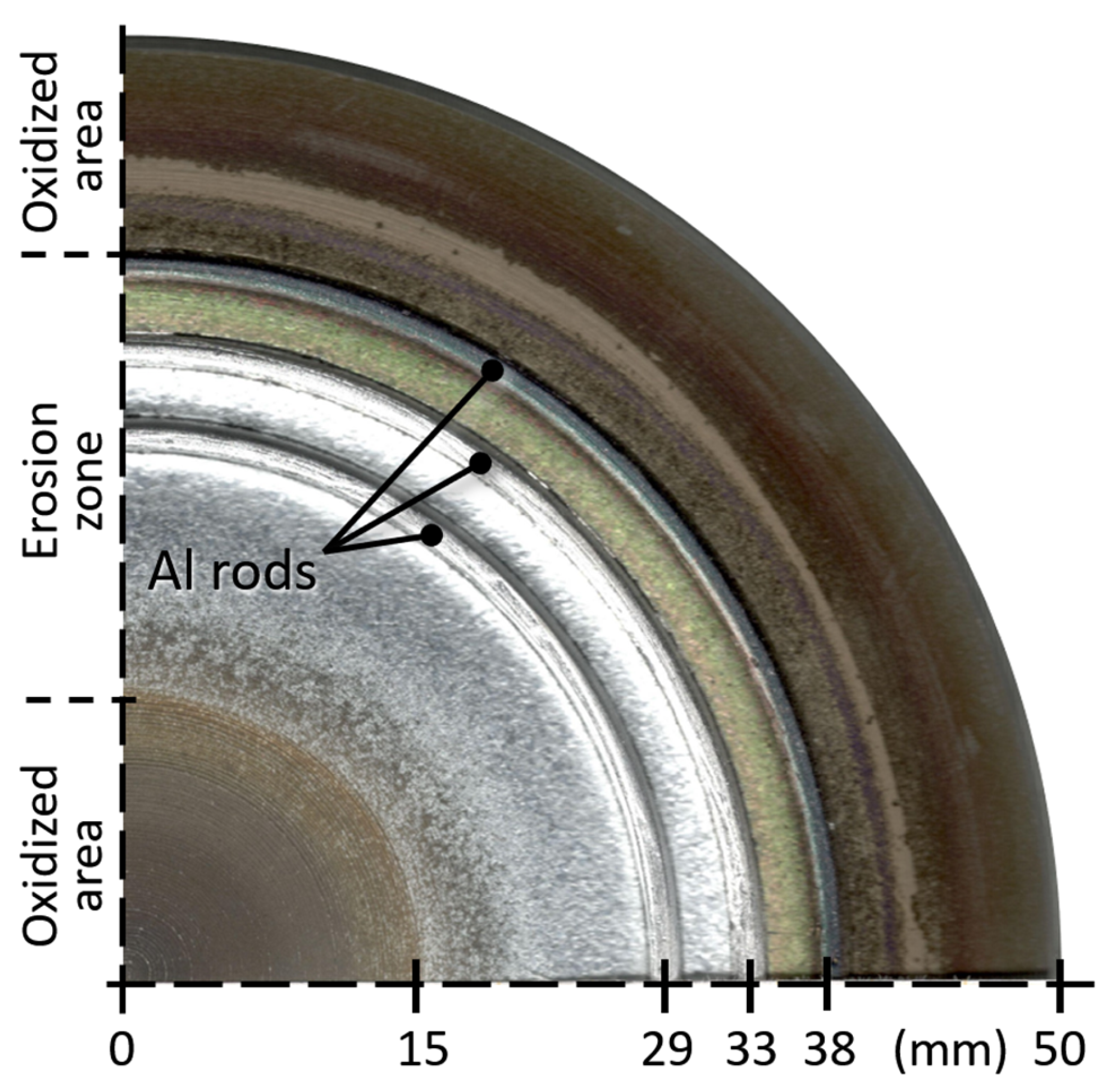
2.4. Two-Element Zn-Al Target

Magnetron co-sputtering is a method that can be used to obtain multi-component films. In the case of binary films, it requires two magnetrons and two power supplies, but it offers the possibility to change the ratio of components in the film over a wide range. Our preliminary studies have shown that the process of deposition of AZO films with TCO properties is sensitive to the ratio of components in the film [20]. Therefore, it is advantageous to employ an approach that offers a narrow possible change to the ratio of components in the film. Utilizing the two-element Zn-Al target, with a fixed ratio of components, imposes a desirable limitation on the aluminum content in the film. Achieving AZO films with TCO properties necessitates precise preparation of the target composition, which will be addressed in this section. As demonstrated in Section 3.3 the results of the aluminum content in the deposited films align closely with the predictions of the sputtering model outlined in this section. The surface view and dimensions of the two-element Zn-Al target (10 mm thick) after several dozen sputtering processes is presented in Figure 1. A distinct erosion zone (race-track region) could be observed, along with dark brown areas covered with non-stoichiometric oxides. The dimensions of the erosion zone, listed below, were similar to prior results [22]. This showed that the geometrical factors of sputtering of such a two-component target are not subject to significant changes. The inner and outer radii of the erosion zone were measured to be about 15 and 39 mm, respectively, resulting in a total erosion zone area of about 4069 mm2. The approximate geometry of the erosion zone (number and location of aluminum rods), suitable for the deposition of AZO films, was estimated experimentally on the basis of previous tests. Based on previous tests, a method for placing rods in the target has also been developed. At a predetermined distance from the center of the target, a dovetail groove is milled. Then, the rod shaped into a circle is inserted into the milled groove. Next, the rod is pressed with a press, so that deformation of the rod takes place, filling the dovetail groove. This procedure ensures low resistance (both electrical and thermal) between the aluminum rode and the zinc disc. The slope of the dovetail is about 10%, which ensures that the composition of the target remains almost constant as the target undergoes successive sputtering processes. There were three aluminum circular inserts (rods) located within the erosion zone. The diameter of the cross-section of each rod was 2 mm, with the radii of their placement successively measuring 29, 33 and 38 mm (Figure 1). Therefore, the zinc area of the erosion zone was about AZn = 2813 mm2. The erosion depth of the Zn area was about 0.9 mm, so it was assumed that the Zn area was flat. The influence of the circular cross-section of the aluminum inserts (rods), in accordance with the angular dependence of the ion-induced sputtering yield, was taken into account during the considerations—the equivalent aluminum area was calculated to be about 5 times larger than that given by the physical dimensions of the inserts. The aluminum rods were slightly flattened during the process of pressing them into the grooves of a zinc disc, so the multiplication factor was assumed to be not greater than 3. The outer aluminum rod was placed on the border of the erosion zone. This fact of the reduced efficiency the of sputtering was taken into account, and, consequently, the multiplication factor was reduced to 1.5 for this rod. The equivalent aluminum area of the erosion zone was finally estimated to be about AAl = 3050 mm2. The estimated areas of Zn and Al, together with the sputtering yield of Zn, Al and their oxides, were utilized for the purpose of deliberation on the conditions of the sputtering of the two-element Zn-Al target.
The wear pattern profile of the target demonstrated that the rate of sputtering in the regions located over the magnetic poles was found to be very low (oxidized areas in Figure 1). Therefore, these regions were found to have minimal impact on considerations of the sputtering conditions. In these regions, the target was observed to be constantly poisoned, and this condition persisted even after short-term transition into full argon sputtering. Based on these observations, it was assumed that considerations about sputtering conditions (induced by the changes of the argon/oxygen ratio) may be simplified and, finally, may be related to the erosion zone only (Figure 1). With that simplified approach, the discharge current was considered to be conducted by the area of erosion zone only—resulting in the target power density (the erosion zone power density) of about 3.7 W/cm2. The energy of the sputtering ions was determined from the oscillogram of anode–cathode voltage. In order to ensure the repeatable ignition of a discharge, the supply pulses of the DPS power unit had an amplitude up to 1.2 kV, with a mean value of about 500 V. Consequently, it was assumed that the sputtering ions had the energy of 500 eV. Based on the Ar/O2 ratios, it was assumed that the discharge current was composed of the argon ions only. In accordance with the literature data, the sputtering yields (molecules, atoms per one incident ion) induced by argon ions were approximately: 5 (Zn), 0.5 (ZnO), 0.9 (Al), 0.5 (Al2O3) [24,25]. The values of the sputtering yields were found to be relatively high, and, for this reason, the interaction of residual and process gases with the surface of the target was assumed to be a minor significance factor that could affect these yields [24]. Furthermore, both the energy and mass of the bombarding ions (argon) were found to be relatively high. Based on these insights, the literature values of sputtering yields were taken directly for further consideration.
In the event of the target operating within an atmosphere rich in oxygen, complete oxidation of the surface is the result, which is known as the dielectric sputtering mode. In such a case, both the zinc and aluminum areas of the erosion zone are oxidized. For the reported investigations, this sputtering condition of the erosion zone (Al2O3, ZnO) is marked as point D in Figure 2. For simplicity, a homogeneous distribution of the discharge current density over the erosion zone can be assumed. With such an assumption, the ratio of sputtered Al2O3/ZnO particles is determined by the ratio of effective aluminum surface area AAl times Al2O3 sputtering yield to zinc surface area AZn times ZnO sputtering yield. For ease of comparison, it is convenient to use the ratio of Al/Zn in the flux to the substrate, which in this case is approximately about 80/100. The films obtained for such a sputtering condition of the target were transparent but showed high resistivity, which was not suitable for the use as a TCO.
If the oxygen content is decreased, then it is possible to reach a state in which the erosion zone is not fully oxidized—known as the transient sputtering mode. In the case of a reported two-element Zn-Al target, the transient mode of sputtering may be considered in yet another way. Since zinc has a higher sputtering yield than aluminum, so the sputtering condition of the erosion zone is likely to be such that the aluminum part operates in the dielectric mode (due to fact that sputtering yield of Al2O3 is 0.2) and the zinc part operates in the transition mode (due to fact that sputtering yield of ZnO is 0.5, more than two times higher than sputtering yield of Al2O3). The zinc oxide that forms is continuously removed, and the metallic zinc surface can be exposed. This is a particular state of dynamic equilibrium, and in fact there can be a different degree of oxidation of the zinc part of the erosion zone. In Figure 2, three cases are indicated, marked as T1, T2 and T3. Each of these cases was obtained by varying the argon/oxygen content ratios: 80/20 (T1), 82/18 (T2) and 84/16 (T3). A change in the degree of oxidation of the target results in a corresponding change in the number of secondary electrons emitted from the target (induced by ion bombardment). The change in secondary electron emission from the target corresponds electrically to a change in the impedance of the magnetron discharge. In the case of materials such as Zn and Al, the increase in oxidation results in an increase in secondary electron emission [26], which in turn leads to a decrease in the impedance of the magnetron discharge. In the case of the DPS power supply, a decrease in the magnetron’s discharge impedance causes an increase in the value of the PC parameter. Because of that, it is notable that, from a technological point of view, there was no requirement to monitor the argon/oxygen ratio during the deposition processes—with the PC value being monitored, for a fixed discharge power of 150 W (Figure 2), the oxygen partial pressure was adjusted to keep the PC value constant. The boundary state may be considered as a sputtering condition of the erosion zone in the form of Zn and Al2O3. In this sputtering condition, the ratio of Al/Zn in the flux to the substrate would be about 9/100. For a sintered AZO target composed of ZnO/Al2O3 98:2 wt%, sputtered in argon [27,28], the Al/Zn ratio in the flux to the substrate is approximately 3/100. It may be noted that the convergence of these ratios (9/100 and 3/100) indicates that our considerations about sputtering of the two-element Zn-Al target seem to be quite likely, even though many simplifying assumptions have been made.
The opposite transient state of the erosion zone of the two-element metallic Zn-Al target, i.e., a sputtering condition of the erosion zone in the form of ZnO and Al, is rather unlikely to occur, because, in the case of such a sputtering condition, the flux of Al/Zn to the substrate would be about 195/100, which does not seem to be applicable for the deposition of transparent AZO films.

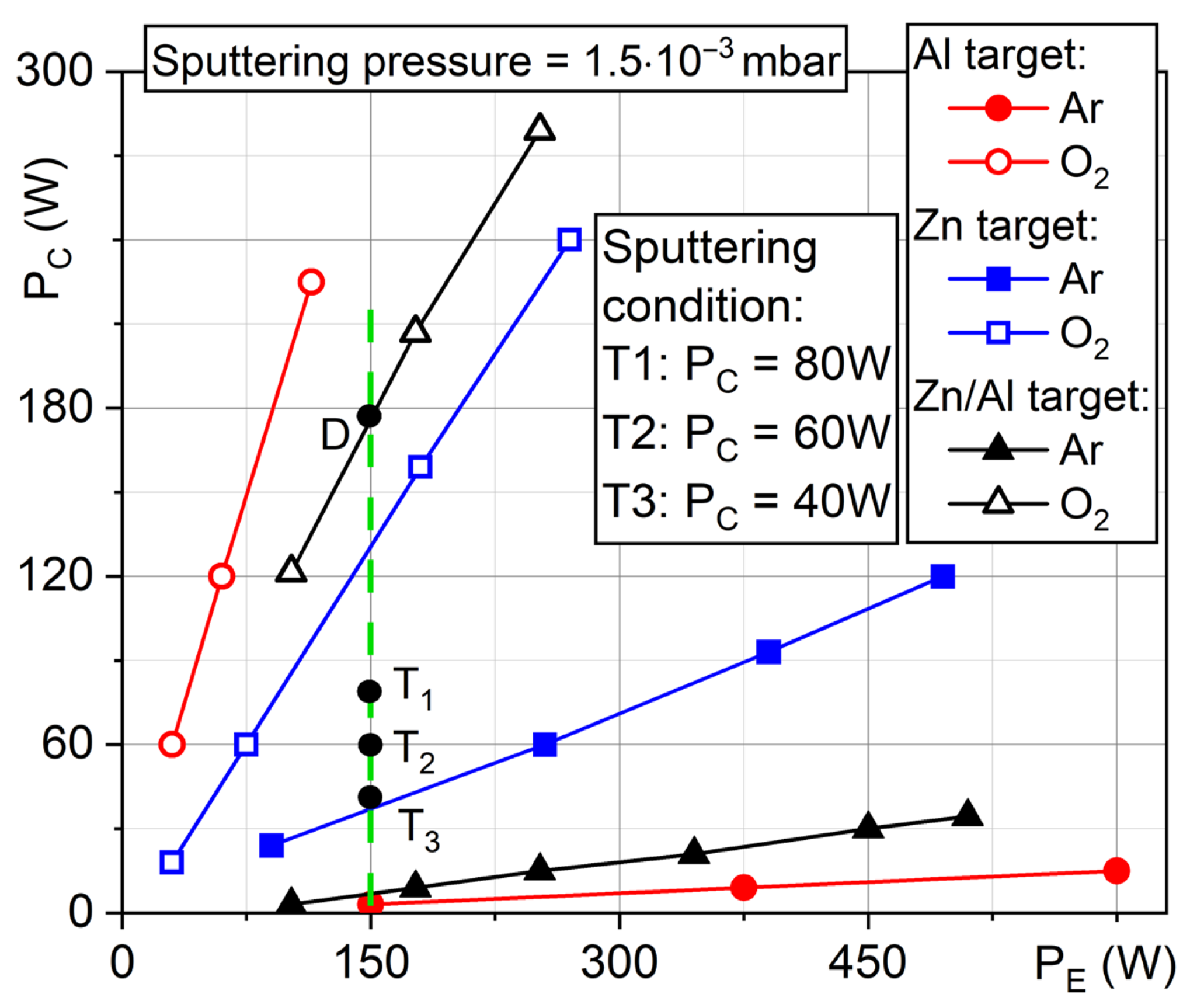
2.5. Monitoring of Sputtering Conditions with DPS Power Supply

The resonance power stage of the DPS power supply is characterized by a specific parameter called circulating power, denoted as PC by the manufacturer. At a given output power value (discharge power value, PE), the value of PC depends on the load impedance [20]. With respect to the sputtering process in an atmosphere of which the argon/oxygen ratio can be changed, the value of PC may be used as the indicator of target’s surface condition (metallic, oxidized) only if there is a difference in the ion-induced secondary electrons emission coefficient between the metallic and oxidized state of the target’s surface. Fortunately, many metals and their oxides exhibit such properties [26], including Zn/ZnO and Al/Al2O3. To illustrate the PC specifics, Figure 2 shows the PC(PE) dependences for a solid Zn target (9 mm thick) sputtered in an argon/oxygen atmosphere of the following ratios: 100/0 (blue line, filled squares)—metallic mode; 0/100 (blue line, open squares)—dielectric mode. For a given discharge power, the oxidation of the zinc target significantly changes the value of PC. Additionally, in that figure, the PC(PE) dependences are shown for a solid Al target (9 mm thick) sputtered in an argon/oxygen atmosphere of the following ratios: 100/0 (red line, filled circles)—metallic mode; 0/100 (red line, open circles)—dielectric mode. The oxidation of the aluminum target changes the PC value even more significantly in comparison to the zinc target. In fact, to monitor the sputtering condition of the target, it is not important to know the value of the ion-induced secondary electron emission coefficient. It is sufficient that the sputtered element has a higher emission of secondary electrons in the oxidized state than in the metallic state—in such a case, an increase in the PC value is present with oxidation of the target.
As the Zn and Al targets showed a change in PC value due to oxidation, it was expected that the two component Zn-Al target would also show this tendency. With respect to the current investigations, in Figure 2 the PC(PE) dependences are shown for a two-element Zn-Al target sputtered in an argon/oxygen atmosphere of the following ratios: 100/0 (black line, filled triangles)—metallic mode; 0/100 (black line, open triangles)—dielectric mode. In this paper, the results obtained at the discharge power of PE = 150 W are reported, which is marked in Figure 2 with a vertical dashed green line. At such a discharge power, the full oxidation of the sputtering zone of the target resulted in a PC value of about 180 W (point D). On the other hand, the metallic state of the sputtering zone resulted in a PC value of about 10 W. As was estimated in the previous section, AZO films suitable as TCO are likely to be deposited while the two-element target is operating in the transient mode. It was concluded that the sputtering condition of the erosion zone may be needed in the form of Zn, Al2O3 to obtain the ratio of Al/Zn in the flux to the substrate to be comparable with the ratio calculated for the sintered AZO target made of ZnO/Al2O3 98:2 wt%. Such a sputtering condition may be achievable rather far from the fully oxidized state. All the estimations made indicated that, for a fixed discharge power of 150 W, the composition of the process atmosphere (argon/oxygen ratio) should be adjusted in such a way that the PC should have a value in the range of 30–90 W. The argon/oxygen ratio was varied, and ratios of 80/20, 82/18 and 84/16 are reported in this paper. In Figure 2 are shown technological points T1 to T3 that correspond to the given argon/oxygen ratio. The given argon/oxygen ratio resulted in PC parameter values of (Figure 2) 80, 60 and 40 W for the Ar/O2 ratios of 80/20 (point T1), 82/18 (point T2) and 84/16 (point T3), respectively. The AZO films, described in the following sections, were obtained at these sputtering conditions to demonstrate the occurrence of optimal conditions for obtaining AZO films with the best TCO properties. The effect of hysteresis influenced the sputtering process. Because of that, the desired argon/oxygen ratio was obtained with a specific procedure—firstly, the oxygen partial pressure was established in the chamber, via needle-type dosing valve, and then argon was added, via another valve, to reach the given total pressure. After the sputtering process was started, the oxygen partial pressure was adjusted to obtain the desired PC value, and the shutter was opened to start the deposition. If the PC value changed during the deposition, then the oxygen partial pressure was changed to restore the desired PC value. This suggests that an automatic regulation loop could be established by linking the dosage of oxygen with the desired PC value, using a similar approach to our previous investigations about deposition of Al2O3 [29].

3. Results

3.1. Transmission of Light

A key performance parameter of films to be suitable for TCO applications is light transmission, particularly in the visible light range. The light transmission characteristics of the as-deposited films at sputtering conditions T1 to T3 (indicated in Figure 2) are shown in Figure 3. For comparison, the transmission spectra of the substrates alone (Corning 7059 glass, Corning Willow® Glass) and ZnO film (400 nm in thickness) are also shown in Figure 3.
The AZO film obtained at sputtering condition T1 (Ar/O2 ratio of 80/20) had a transmission higher than 80% in the 450–2000 nm wavelength range (flexible glass substrate). The film deposited on standard glass substrate had a slightly lower transmission coefficient, especially in the 1000–2000 nm wavelength range (77%). The transmission coefficient value did not fluctuate significantly throughout the measured range, for both substrate types. The highest value of transmission coefficient (of about 90%) was found in the 525–600 nm wavelength range. In the visible wavelength range, the average transmission of light was calculated to be approximately 84%. For comparison, the average transmission of light of the ZnO film (400 nm in thickness) was calculated to be about 82%, which was in good agreement with other reports [30,31]. The AZO film obtained at sputtering condition T2 (Ar/O2 ratio of 82/18) had a transmission higher than 80% in the 450–1150 nm wavelength range, for both substrate types. Within this range, the results were found to be similar to the film obtained at sputtering condition T1. That resulted in the calculated average transmission of light in the visible wavelength range to be about 83%. A significant decrease in the transmission was observed for wavelengths longer than 1250 nm, but it did not decline below 55%, up to 2000 nm. Such an observed decrease in transmittance in the near-infrared range was caused by the conductive property of the charge carriers in AZO [30,31,32]. The AZO film obtained at sputtering condition T3 (Ar/O2 ratio of 84/16) had the lowest (of all samples) light transmission, over the entire measured range. In the 450–1150 nm range, it had a transmission of approximately 70%. In the visible wavelength range, the average transmission of light was calculated to be about 67%. Similarly to the sample obtained at sputtering condition T2, the transmission significantly decreased for wavelengths above 1250 nm. However, it did not decrease below 50%, up to 2000 nm. The results of the transmission measurements are summarized in Table 1, together with the calculated values of the fundamental absorption edge (the cut-off wavelength).

3.2. Electrical Properties—Resistivity

Measurements of the sheet resistance were performed for the as-deposited samples. The sheet resistance, together with the film thickness, were used to calculate the resistivity of the AZO films, and the calculations results are summarized in Table 1. The AZO films with the lowest resistivity (close to the 10−4 Ω·cm range) were obtained at sputtering condition T2 (Ar/O2 ratio of 82/18).
To evaluate the TCO quality of the deposited films, the Figure of Merit (FOM) was calculated. This provided a valuable metric, taking into account both the electrical and optical properties of the films, using the modified Haacke formula, FOM = T10/ρ [33], where T is the average light transmittance in the visible spectrum, and ρ is the resistivity of the film (Ω·cm). The highest FOM values were obtained for films deposited at sputtering condition T2 (Ar/O2 ratio of 82/18). Additionally, a positive influence of the substrate was observed—the sample prepared on flexible glass had the best optical and electrical properties.

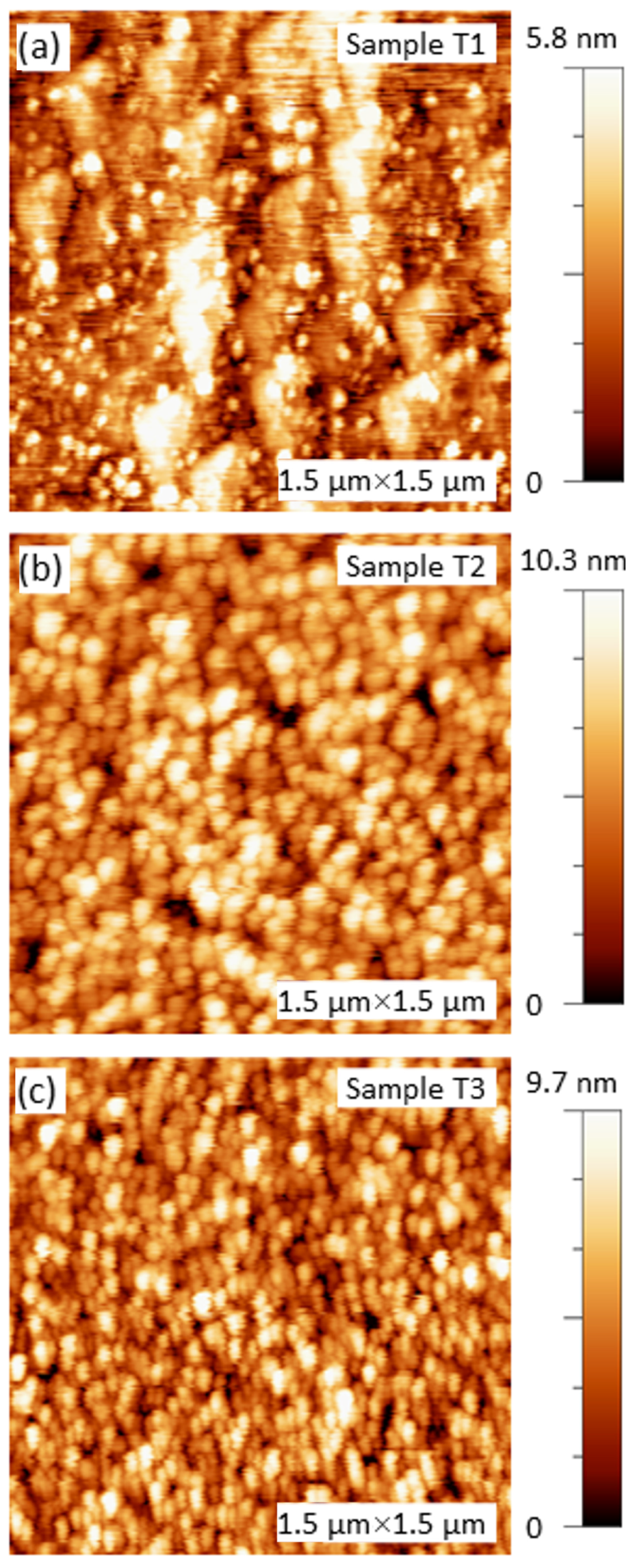
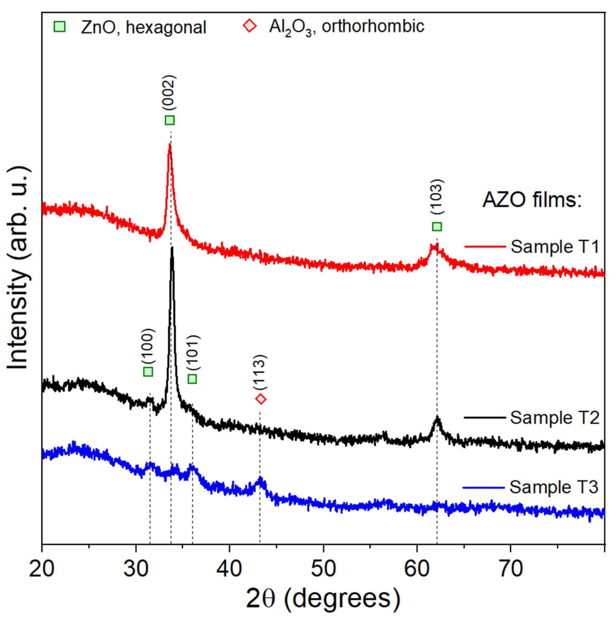
3.3. Surface Properties, Elemental Composition and Microstructure

The deposited films were diagnosed using SEM microscopy for surface imaging (Figure 4). The surface morphology was diagnosed based on the AFM scans (Figure 5). The results of EDS measurements are presented in Figure 6. Table 2 and Table 3 present the quantitative results of these measurements. Both SEM and AFM scans showed that the surface of the films, deposited in each of the three sputtering conditions (T1, T2 and T3), had a smooth surface. Rare aggregations of material were found only on the sample T2 (standard glass). The EDS images showed uniform distribution of elements over the whole area of samples; no imprints of the geometric distribution of Zn-Al elements from the target were present on the samples. It can be concluded that the distance between the target and substrate, together with the geometric features of deposition process, were sufficient for the discharge plasma to cause mixing of sputtered material.
The results summarized in Table 2 show that the variation of the Ar/O2 ratio did not significantly affect the surface morphology of the obtained AZO films in the studied range of Ar/O2 ratios. However, the films had the lowest surface roughness values under the T1 sputtering condition. Unfortunately, the T1 sputtering condition resulted in the highest resistivity of the obtained films (Table 1).
Based on the EDS measurements (Figure 6, Table 3), the ratio of Al/Zn atoms in the films was calculated (Table 3). The resulting values were in good agreement with the theoretical predictions given in Section 2 for the boundary state of the erosion zone in the form of Zn, Al2O3. For this sputtering condition, the ratio of Al/Zn in the flux to the substrate was estimated to be about 9/100.
The diffraction patterns of the AZO films obtained at technological points T1, T2 and T3 are shown in Figure 7. All the samples showed a nanocrystalline structure. The most intense peaks related to the ZnO hexagonal phase (PDF card 65-3411) were found for the T2 sample, which may indicate the most crystallized structure among all the deposited films. The most intense peak in the case of T1 and T2 samples was (002), and the crystallite sizes calculated using Debye–Scherrer equation were 10.2 and 13.9 nm, respectively. Diffraction patterns for sample T2 also showed the occurrence of (100) and (101) ZnO hexagonal planes. The samples T1 and T2 demonstrated similar transmittance for the visible range (of about 80%), but the resistivity of the T2 sample was about thirty times lower than resistivity of the T1 sample (Table 1). It may be suggested that an increase in the size of the crystallites (002) accompanied by the remarkable presence of (100) and (101) planes had a positive effect on decreasing the resistivity of the AZO film.
In addition, sample T3 also revealed a rhombohedral Al2O3 phase with a peak at about 43.4° corresponding to the (113) plane. For this sample, the ZnO crystallite size (calculated for the (101) plane) was 9.3 nm, and the Al2O3 crystallite size (calculated for the (113) plane) was 9.1 nm. The samples T2 and T3 demonstrated similar resistivity (lower than 2·10−3 Ω·cm), but the transmittance of the T3 sample was about 15% lower than the transmittance of the T2 sample (Table 1). Limited oxidation of the sample T3 (due to a high Ar/O2 ratio, Table 1) was insufficient to form a dominating ZnO crystallites (002) plane (Figure 7), and the (113) Al2O3 became present. The appearance of the T3 sample exhibited a dark gray shade, typical of under-oxidized aluminum oxide. The presence of non-oxidized aluminum in the film could be a reason of its low resistivity—according to Table 3, the T3 sample had the highest aluminum/zinc ratio.

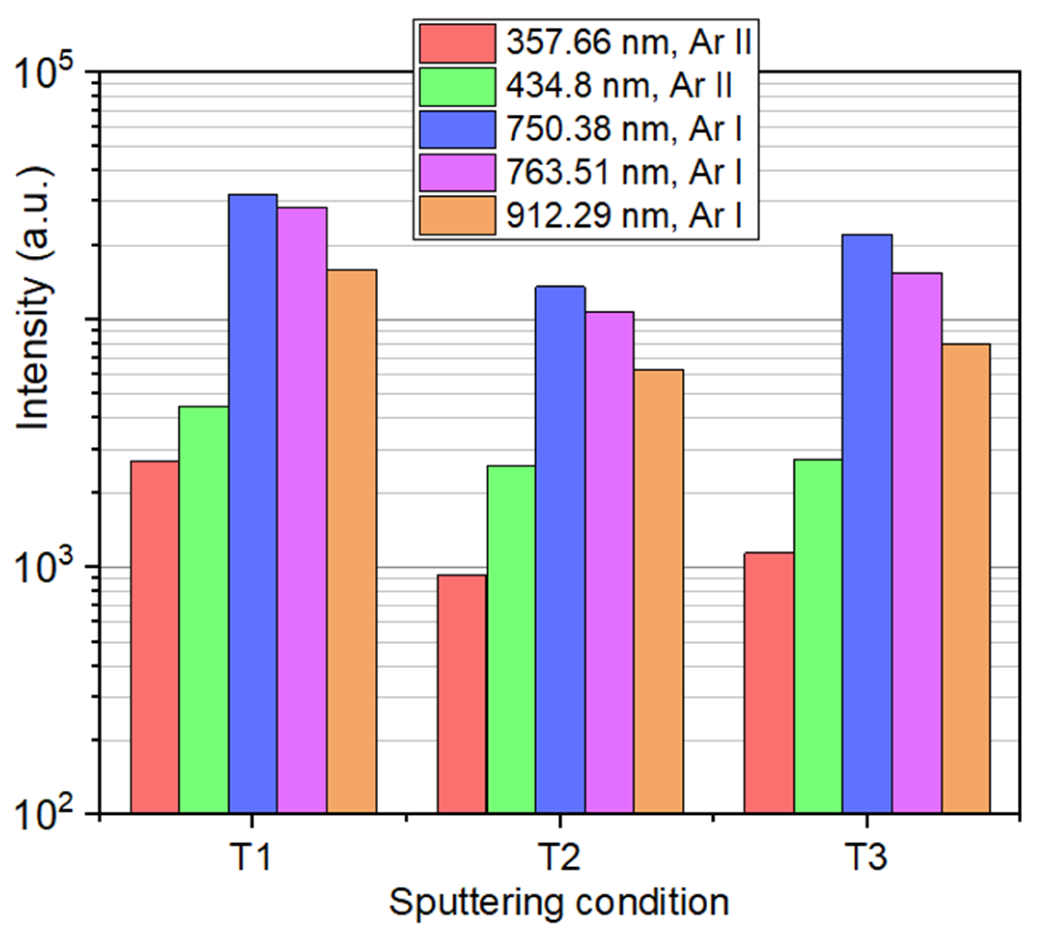
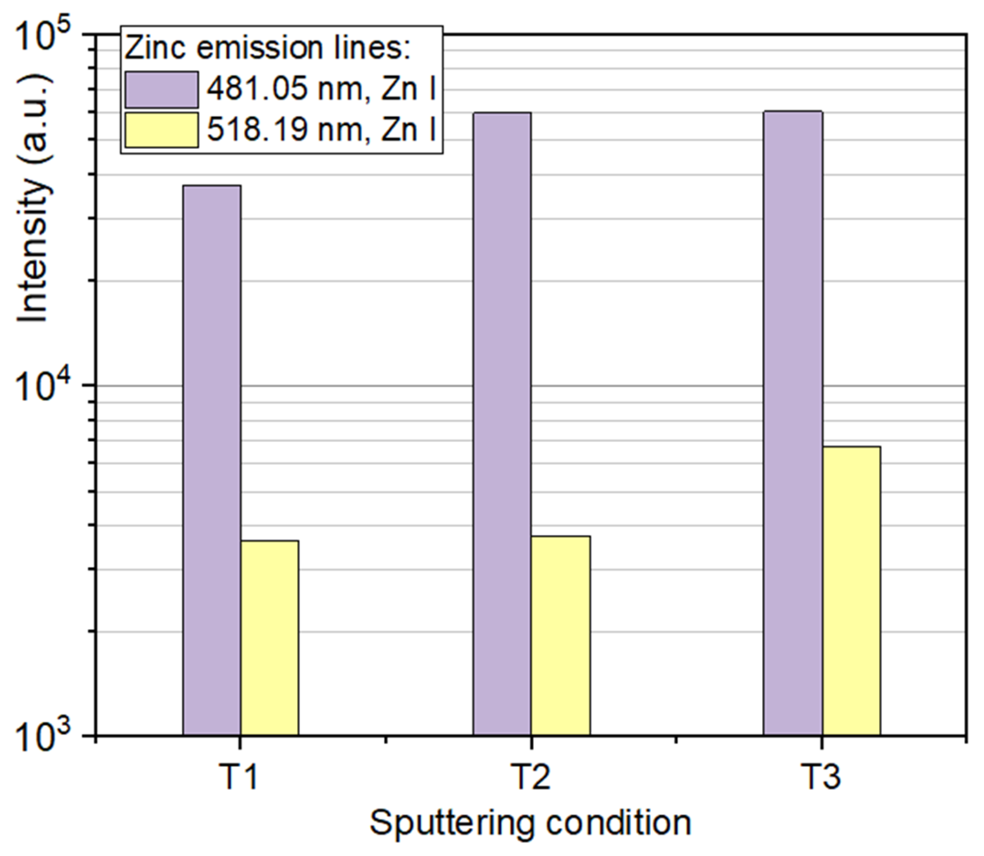
3.4. Optical Emission of Plasma (OES)

The results of these studies of the optical and electrical parameters of the obtained AZO films have shown that there is a certain optimum of reactive gas dosage (given by sputtering condition T2), which enables deposition of AZO films with TCO properties to be obtained using developed two-element Zn-Al target. When using the DORA medium frequency power supply, this point of the optimum Ar/O2 ratio can be easily maintained by controlling the value of the circulating power PC, which is read from the power supply during the sputtering process. As the DORA medium frequency power supply is used rather locally in the manufacturer’s country, an OES diagnostic was undertaken to investigate whether the indication of the optimum reactive gas dosage could be realized independently of the magnetron power supply used. For sputtering processes described with the T1, T2 and T3 conditions, the plasma emission spectra were recorded using a low-cost spectrophotometer. Spectral lines that could be clearly identified were selected in the recorded OES spectra—unfortunately, there were not many of them. Among these identified lines, we searched for those lines whose intensity varied in a characteristic way among conditions T1 to T3, so that some mechanism for controlling the sputtering process could be proposed. In the case of argon spectral lines, some lines of excited atoms and ions were found, which showed the minimum intensity for the T2 conditions (Figure 8).
In the case of zinc (Figure 9), two spectral lines were selected, the intensity of which changed in a characteristic manner among conditions T1 to T3., whose intensity varied in a characteristic way among conditions T1 to T3. The 481.05 nm line of excited atoms indicated an intensity increase on the change of sputtering conditions from T1 to T2. The transition from T2 to T3 sputtering conditions did not affect the intensity of this line. On the other hand, the intensity of the 518.19 nm line was not affected by the transition from T1 to T2 sputtering conditions, while the transition from T2 to T3 sputtering conditions caused an intensity increase.
As mentioned at the beginning of this section, the OES measurements were not carried out to study the energy conditions in the plasma but to verify whether there were any emission lines exhibiting a notable change in intensity in the range of the T1 to T3 conditions. This would facilitate the identification of an alternative stabilization method—one that would not rely on the PC parameter of the DPS power supply. The observation that, among the easily identifiable emission lines of the plasma components, only a few lines showed characteristic intensity change suggests that the energy conditions in the plasma are subtly dependent on the technological point of obtaining AZO layers within the transition mode. Studies of such dependence were not in the main scope of the reported investigations.

4. Discussion and Conclusions

In this work, the concept of a self-designed two-element Zn-Al target is presented, with the purpose of obtaining AZO films with parameters suitable for TCO applications. The deposition processes were carried out at room temperature—no additional heating of the substrates was introduced. Such an approach was intentionally applied because we would like to use this type of film in a flexible semiconductor device on a low-cost substrate, such as PET. The ratio of aluminum to zinc incorporated in the target was determined by a simple analysis of the sputtering mechanism for the transient mode. The ratio of Al/Zn atoms in the material flux to the substrate was analyzed in relation to the degree of oxidation of the target’s erosion zone. It was estimated that AZO films with TCO properties could be deposited if the erosion zone of the target was operating at a specific sputtering condition related to the transient sputtering mode. It was suggested that this specific sputtering condition included full oxidation of the aluminum part, while the Zn part was in a transient mode located close to the metallic sputtering mode. In such a case, the Al/Zn ratio was calculated to be comparable to the Al/Zn ratio obtained in the material flux from the sintered AZO target made of ZnO/Al2O3, 98:2.
This paper presents a fragment of broader studies of the sputtering of two-element Zn-Al targets in transition modes. Here, the AZO films were deposited for the selected three argon/oxygen ratios in a sputtering process atmosphere. A DPS supply was used to power the magnetron source, which allowed the oxidation state of the target to be monitored based on the value of the PC parameter. Thus, it was not necessary to maintain the argon/oxygen ratio during the sputtering process but only to maintain a specific value of the PC parameter by correcting the oxygen inflow rate. For this reason, the use of a DPS power supply unit naturally enabled the feature that the oxygen dosage could be linked via a control loop to the electrical parameter of the power supply. Alternatively, several OES plasma emission lines were also indicated, which could also be used to stabilize the sputtering process, but such a control loop was not tested. Especially, selected argon lines were shown to be suitable for that, because local minimum intensity was observed.
At the discharge power of 150 W, the argon/oxygen ration of about 82/18% resulted in the lowest resistivity and highest transmittance (for the visible range) of the obtained AZO films, and the values were of about 1.2·10−3 Ω·cm and 85%, respectively. This formed the specific sputtering condition that could be easily determinedusing the relation of the discharge power and parameter of the DPS power supply (circulating power), which were linked by the relationship of PC/PE ≈ 0.5. Other preliminary work has shown that this relationship was valid for the discharge power up to approximately 400 W, demonstrating that the process of deposition of AZO films from a two-element Zn-Al target seemed to be scalable.
Fortunately, the aluminum rods incorporated in the Zn-Al target in the oxidized state do not introduce the arcing problem. The use of pulsed sputtering (100 kHz) and low target power density in the erosion zone (3.7 W/cm2) seems to make it possible to effectively neutralize the charge of sputtering ions accumulating on oxidized aluminum—Figure 4 presents a smooth film surface, with no micro-droplets inclusions, and the calculated RMS roughness was lower than 2 nm (Table 2). In the case of poor neutralization, arcing would occur on the target (aluminum rods), and the deposited film would have micro-droplet inclusions, which is often observed as a problem in high target power deposition processes [29].

Author Contributions

Conceptualization, S.K., A.W. and W.P.; methodology, S.K. and A.W.; formal analysis, A.W. and J.D.; investigation, S.K., A.W. and M.M. (XRD); writing—original draft preparation, S.K.; writing—review and editing, A.W. and J.D. All authors have read and agreed to the published version of the manuscript.

Funding

This work was financed from the internal sources of Wroclaw University of Science and Technology.

Institutional Review Board Statement

Not applicable.

Informed Consent Statement

Not applicable.

Data Availability Statement

The original contributions presented in this study are included in the article. Further inquiries can be directed to the corresponding author(s).

Conflicts of Interest

The authors declare no conflicts of interest.

References

  1. Kelly, P.J.; Arnell, R.D. Magnetron Sputtering: A Review of Recent Developments and Applications. Vacuum 2000, 56, 159–172. [Google Scholar] [CrossRef]
  2. McLeod, P.S.; Hartsough, L.D. High-rate Sputtering of Aluminum for Metallization of Integrated Circuits. J. Vac. Sci. Technol. 1977, 14, 263–265. [Google Scholar] [CrossRef]
  3. Waits, R.K. Planar Magnetron Sputtering. J. Vac. Sci. Technol. 1978, 15, 179–187. [Google Scholar] [CrossRef]
  4. Gao, Z.; Banerjee, P. Review Article: Atomic Layer Deposition of Doped ZnO Films. J. Vac. Sci. Technol. A Vac. Surf. Film. 2019, 37, 050802. [Google Scholar] [CrossRef]
  5. Minami, T. Transparent Conducting Oxide Semiconductors for Transparent Electrodes. Semicond. Sci. Technol. 2005, 20, S35–S44. [Google Scholar] [CrossRef]
  6. Liu, Y.; Li, Y.; Zeng, H. ZnO-Based Transparent Conductive Thin Films: Doping, Performance, and Processing. J. Nanomater. 2013, 2013, 196521. [Google Scholar] [CrossRef]
  7. Liu, C.C.; Chen, Y.S.; Huang, J.J. High-Performance ZnO Thin-Film Transistors Fabricated at Low Temperature on Glass Substrates. Electron. Lett. 2006, 42, 824–825. [Google Scholar] [CrossRef]
  8. Asenjo, B.; Chaparro, A.M.; Gutiérrez, M.T.; Herrero, J.; Klaer, J. Study of CuInS2/Buffer/ZnO Solar Cells, with Chemically Deposited ZnS-In2S3 Buffer Layers. Thin Solid Film. 2007, 515, 6036–6040. [Google Scholar] [CrossRef]
  9. Yang, J.; Park, J.K.; Kim, S.; Choi, W.; Lee, S.; Kim, H. Atomic-layer-deposited ZnO Thin-film Transistors with Various Gate Dielectrics. Phys. Status Solidi 2012, 209, 2087–2090. [Google Scholar] [CrossRef]
  10. Wang, J.-C.; Weng, W.-T.; Tsai, M.-Y.; Lee, M.-K.; Horng, S.-F.; Perng, T.-P.; Kei, C.-C.; Yu, C.-C.; Meng, H.-F. Highly Efficient Flexible Inverted Organic Solar Cells Using Atomic Layer Deposited ZnO as Electron Selective Layer. J. Mater. Chem. 2010, 20, 862–866. [Google Scholar] [CrossRef]
  11. Chen, H.-C.; Chen, M.-J.; Wu, M.-K.; Li, W.-C.; Tsai, H.-L.; Yang, J.-R.; Kuan, H.; Shiojiri, M. UV Electroluminescence and Structure of N-ZnO/p-GaN Heterojunction LEDs Grown by Atomic Layer Deposition. IEEE J. Quantum Electron. 2010, 46, 265–271. [Google Scholar] [CrossRef]
  12. Elam, J.W.; Sechrist, Z.A.; George, S.M. ZnO/Al2O3 Nanolaminates Fabricated by Atomic Layer Deposition: Growth and Surface Roughness Measurements. Thin Solid Film. 2002, 414, 43–55. [Google Scholar] [CrossRef]
  13. Kim, K.H.; Park, K.C.; Ma, D.Y. Structural, Electrical and Optical Properties of Aluminum Doped Zinc Oxide Films Prepared by Radio Frequency Magnetron Sputtering. J. Appl. Phys. 1997, 81, 7764–7772. [Google Scholar] [CrossRef]
  14. Agashe, C.; Kluth, O.; Schöpe, G.; Siekmann, H.; Hüpkes, J.; Rech, B. Optimization of the Electrical Properties of Magnetron Sputtered Aluminum-Doped Zinc Oxide Films for Opto-Electronic Applications. Thin Solid Film. 2003, 442, 167–172. [Google Scholar] [CrossRef]
  15. Banerjee, P.; Lee, W.-J.; Bae, K.-R.; Lee, S.B.; Rubloff, G.W. Structural, Electrical, and Optical Properties of Atomic Layer Deposition Al-Doped ZnO Films. J. Appl. Phys. 2010, 108, 043504. [Google Scholar] [CrossRef]
  16. Nam, T.; Lee, C.W.; Kim, H.J.; Kim, H. Growth Characteristics and Properties of Ga-Doped ZnO (GZO) Thin Films Grown by Thermal and Plasma-Enhanced Atomic Layer Deposition. Appl. Surf. Sci. 2014, 295, 260–265. [Google Scholar] [CrossRef]
  17. Barhoumi, A.; Leroy, G.; Duponchel, B.; Gest, J.; Yang, L.; Waldhoff, N.; Guermazi, S. Aluminum Doped ZnO Thin Films Deposited by Direct Current Sputtering: Structural and Optical Properties. Superlattices Microstruct. 2015, 82, 483–498. [Google Scholar] [CrossRef]
  18. Yamamoto, T.; Katayama-Yoshida, H. Physics and Control of Valence States in ZnO by Codoping Method. Phys. B Condens. Matter 2001, 302–303, 155–162. [Google Scholar] [CrossRef]
  19. Ellmer, K.; Bikowski, A. Intrinsic and Extrinsic Doping of ZnO and ZnO Alloys. J. Phys. D Appl. Phys. 2016, 49, 413002. [Google Scholar] [CrossRef]
  20. Posadowski, W.; Wiatrowski, A.; Domaradzki, J.; Mazur, M. Selected Properties of AlxZnyO Thin Films Prepared by Reactive Pulsed Magnetron Sputtering Using a Two-Element Zn/Al Target. Beilstein J. Nanotechnol. 2022, 13, 344–354. [Google Scholar] [CrossRef]
  21. Posadowski, W.M.; Wiatrowski, A.; Dora, J.; Radzimski, Z.J. Magnetron Sputtering Process Control by Medium-Frequency Power Supply Parameter. Thin Solid Film. 2008, 516, 4478–4482. [Google Scholar] [CrossRef]
  22. Kiełczawa, S. Specific Method of Deposition of Aluminium-Doped Zinc Oxide Thin Films on Flexible Glass Substrates. Electrotech. Rev. 2022, 1, 249–252. [Google Scholar] [CrossRef]
  23. Klug, H.P.; Alexander, L.E. X-Ray Diffraction Procedures: For Polycrystalline and Amorphous Materials; Wiley: New York, NY, USA, 1976; ISBN 978-0-471-49369-3. [Google Scholar]
  24. Eckstein, W. Sputtering Yields. In Sputtering by Particle Bombardment; Topics in Applied Physics; Springer: Berlin/Heidelberg, Germany, 2007; Volume 110, pp. 33–187. ISBN 978-3-540-44500-5. [Google Scholar]
  25. Tominaga, K.; Ueshiba, N.; Shintani, Y.; Tada, O. High-Energy Neutral Atoms in the Sputtering of ZnO. Jpn. J. Appl. Phys. 1981, 20, 519. [Google Scholar] [CrossRef]
  26. Depla, D.; Heirwegh, S.; Mahieu, S.; Haemers, J.; De Gryse, R. Understanding the Discharge Voltage Behavior during Reactive Sputtering of Oxides. J. Appl. Phys. 2007, 101, 013301. [Google Scholar] [CrossRef]
  27. Subramanyam, T.K.; Goutham, P.; Pavan Kumar, S.; Yadhuraj, S.R.; Geetha, K.S. Optimization of Sputtered AZO Thin Films for Device Application. Mater. Today Proc. 2018, 5, 10851–10859. [Google Scholar] [CrossRef]
  28. Bussell, B.C.; Gibson, P.N.; Lawton, J.; Couture, P.; Sharpe, M.K.; England, J.; Hinder, S.J.; Stolojan, V.; Thornley, S.A.; Baker, M.A. The Effect of RF Plasma Power on Remote Plasma Sputtered AZO Thin Films. Surf. Coat. Technol. 2022, 442, 128402. [Google Scholar] [CrossRef]
  29. Wiatrowski, A.; Patela, S.; Kunicki, P.; Posadowski, W. Effective Reactive Pulsed Magnetron Sputtering of Aluminium Oxide—Properties of Films Deposited Utilizing Automated Process Stabilizer. Vacuum 2016, 134, 54–62. [Google Scholar] [CrossRef]
  30. Qiao, Z.; Agashe, C.; Mergel, D. Dielectric Modeling of Transmittance Spectra of Thin ZnO:Al Films. Thin Solid Film. 2006, 496, 520–525. [Google Scholar] [CrossRef]
  31. Hsu, J.-C.; Chen, Y.-Y. Comparison of the Optical and Electrical Properties of Al-Doped ZnO Films Using a Lorentz Model. Coatings 2018, 9, 4. [Google Scholar] [CrossRef]
  32. Kumar, P.; Dharmaprakash, S.M. A Comparative Analysis of Structural, Optical, and Electrical Characteristics of c-Plane and a-Plane ZnO:Al Thin Films Fabricated by a Pulsed Laser Ablation Technique. Appl. Surf. Sci. 2022, 593, 153423. [Google Scholar] [CrossRef]
  33. Haacke, G. New Figure of Merit for Transparent Conductors. J. Appl. Phys. 1976, 47, 4086–4089. [Google Scholar] [CrossRef]
Figure 1. A sectional view of the two-component Zn-Al metallic target; the dimensions of the erosion zone and placement of the aluminum rods are given.
Coatings 15 00713 g001
Figure 2. The circulating power PC dependence on discharge power PE at different target material and composition of the sputtering atmosphere. Technological points T1 to T3 are described in Section 2.4.
Coatings 15 00713 g002
Figure 3. Transmission spectra of obtained AZO films.
Coatings 15 00713 g003
Figure 4. SEM scans of obtained AZO films deposited on standard glass substrates. Argon/oxygen ratio: 80/20 (a), 82/18 (b), 84/16 (c).
Coatings 15 00713 g004
Figure 5. AFM scans of obtained AZO films deposited on standard glass substrates. Argon/oxygen ratio: 80/20 (a), 82/18 (b), 84/16 (c).
Coatings 15 00713 g005
Figure 6. EDS scans of obtained AZO films deposited on amorphous silica substrates. Argon/oxygen ratio: 80/20 (a), 82/18 (b), 84/16 (c).
Coatings 15 00713 g006
Figure 7. X-ray diffraction results of deposited AZO thin films.
Coatings 15 00713 g007
Figure 8. Selected spectral lines of argon that exhibit minimum intensity during transition of sputtering process among conditions T1 to T3.
Coatings 15 00713 g008
Figure 9. Intensity change of selected zinc spectral lines as a function of transition of sputtering process among conditions T1 to T3.
Coatings 15 00713 g009
Table 1. Electrical and optical parameters of obtained AZO films.
SampleFilm Thickness
(nm)
Sheet Resistance
(Ω/sq.)
Resistivity
10−3
(Ω·cm)
Cut-Off Wavelength
(nm)
Transmittance (Avg. Value for VIS Range) %Figure of Merit
(1/Ω·cm)
SubstrateAr/O2 Ratio %
Standard glass
(Corning)
T1 (80/20)88539147.4326844
T2 (82/18)1161211.430683110
T3 (84/16)1231571.9305657
Flexible glass
(Willow)
T1 (80/20)88389634.3300866
T2 (82/18)1161001.229485167
T3 (84/16)1231351.72957017
Table 2. Surface properties of obtained AZO films.
SampleRMS Roughness
(nm)
Peak-to-Peak
(nm)
SubstrateAr/O2 Ratio %
Standard glass
(Corning)
T1 (80/20)1.345.8
T2 (82/18)1.8610.3
T3 (84/16)1.819.7
Flexible glass
(Willow)
T1 (80/20)1.215.6
T2 (82/18)1.427.8
T3 (84/16)1.618.5
Table 3. Elemental composition of obtained AZO films (amorphous silica substrate).
PC40 W (T3)60 W (T2)80 W (T1)
ElementAtomic NumberMass Normalized [%]Atom [%]Mass Normalized [%]Atom [%]Mass Normalized [%]Atom [%]
Al130.60.600.50.560.50.57
Zn3013.86.2217.68.0315.46.94
Si1481.485.376.881.979.183.3
O84.37.855.19.555.09.23
Al/Zn ratio 10/100 7/100 8/100
Disclaimer/Publisher’s Note: The statements, opinions and data contained in all publications are solely those of the individual author(s) and contributor(s) and not of MDPI and/or the editor(s). MDPI and/or the editor(s) disclaim responsibility for any injury to people or property resulting from any ideas, methods, instructions or products referred to in the content.

