

Quality and Lifetime of Thin Parylene F-VT4 Coatings for Hermetic Encapsulation of Implantable Medical Devices


Abstract

1. Introduction
2. Materials and Methods
2.1. Sample Preparation
2.2. Pinhole Test
2.3. Accelerated Aging
2.4. Experimental Setup for EIS
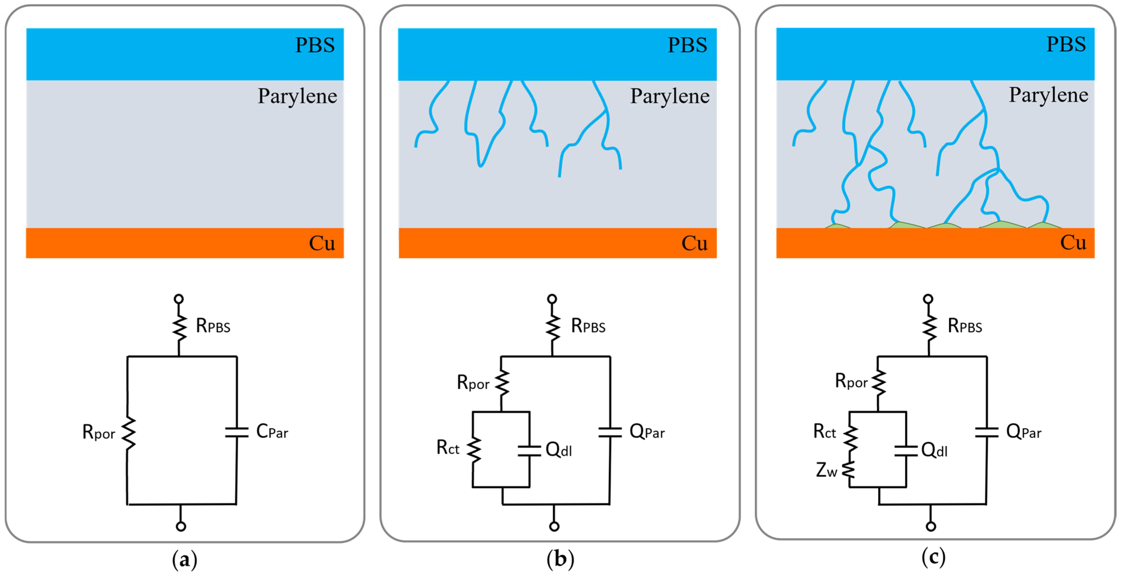
2.5. Equivalent Circuit Modeling
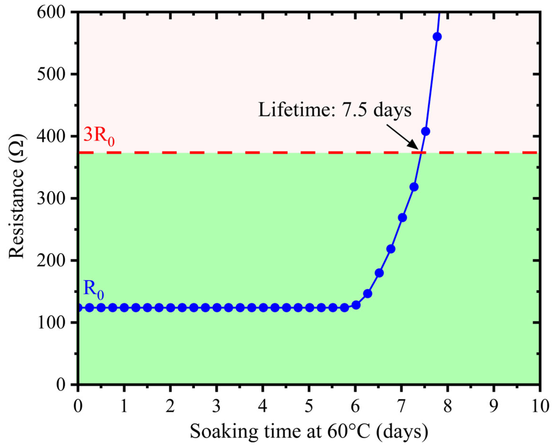
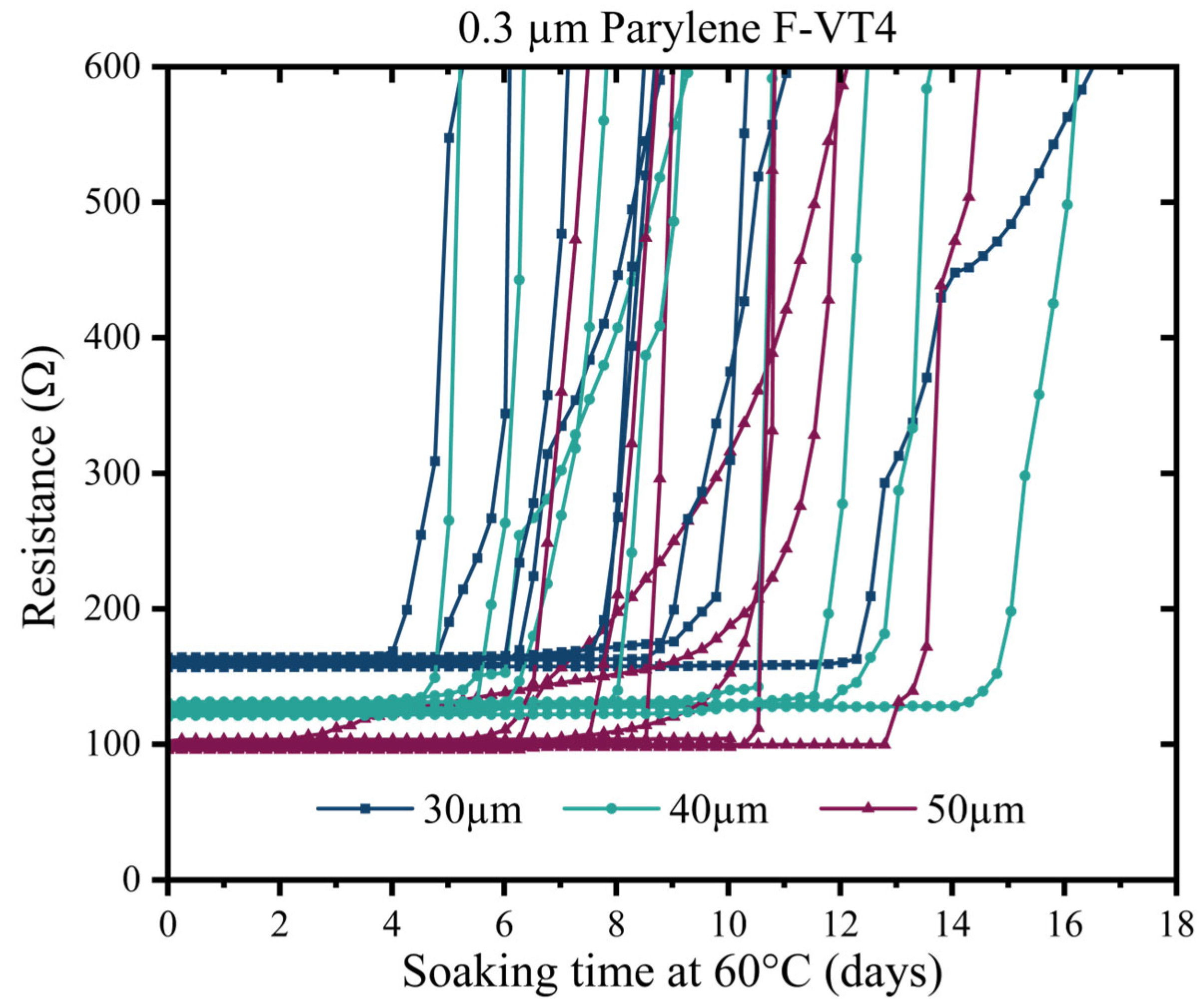
2.6. Resistance-Based Lifetime Testing
3. Results and Discussion
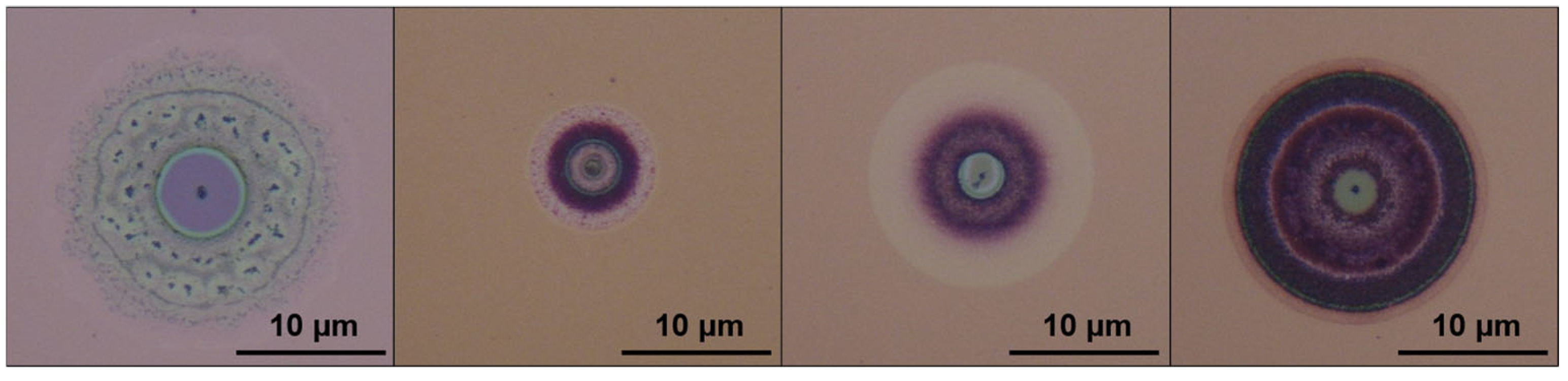
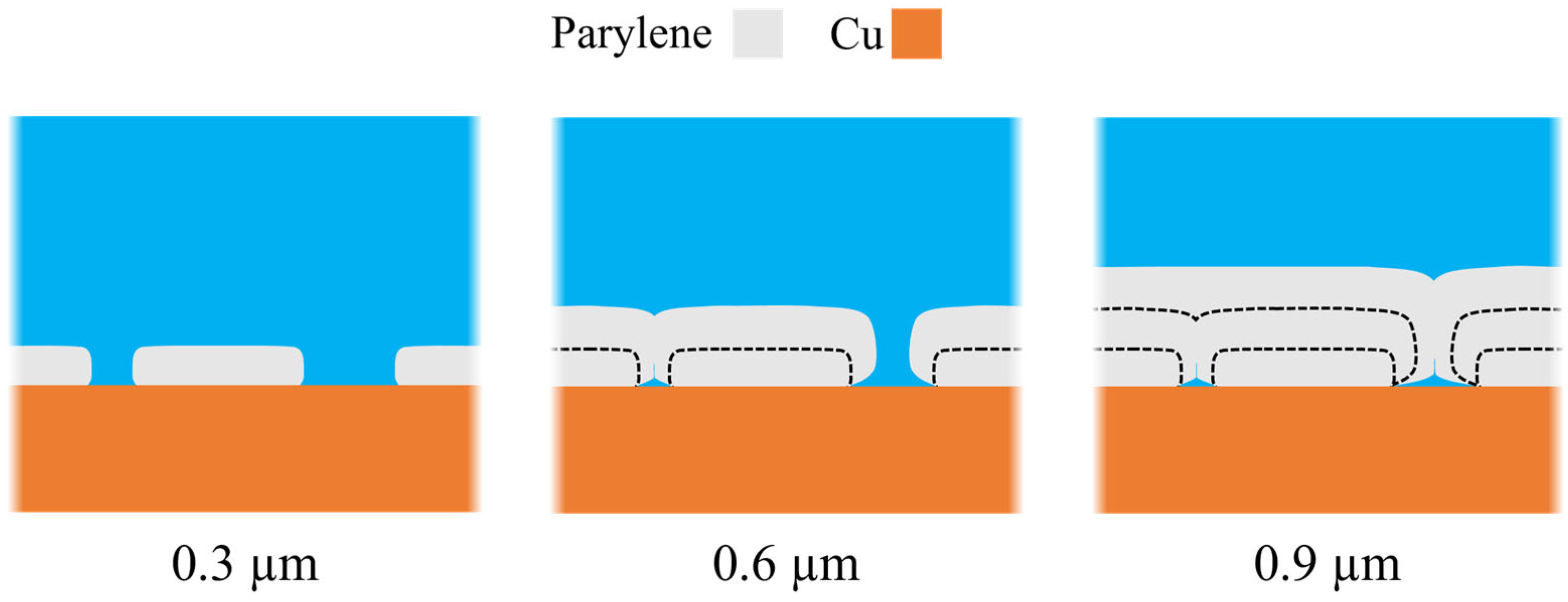
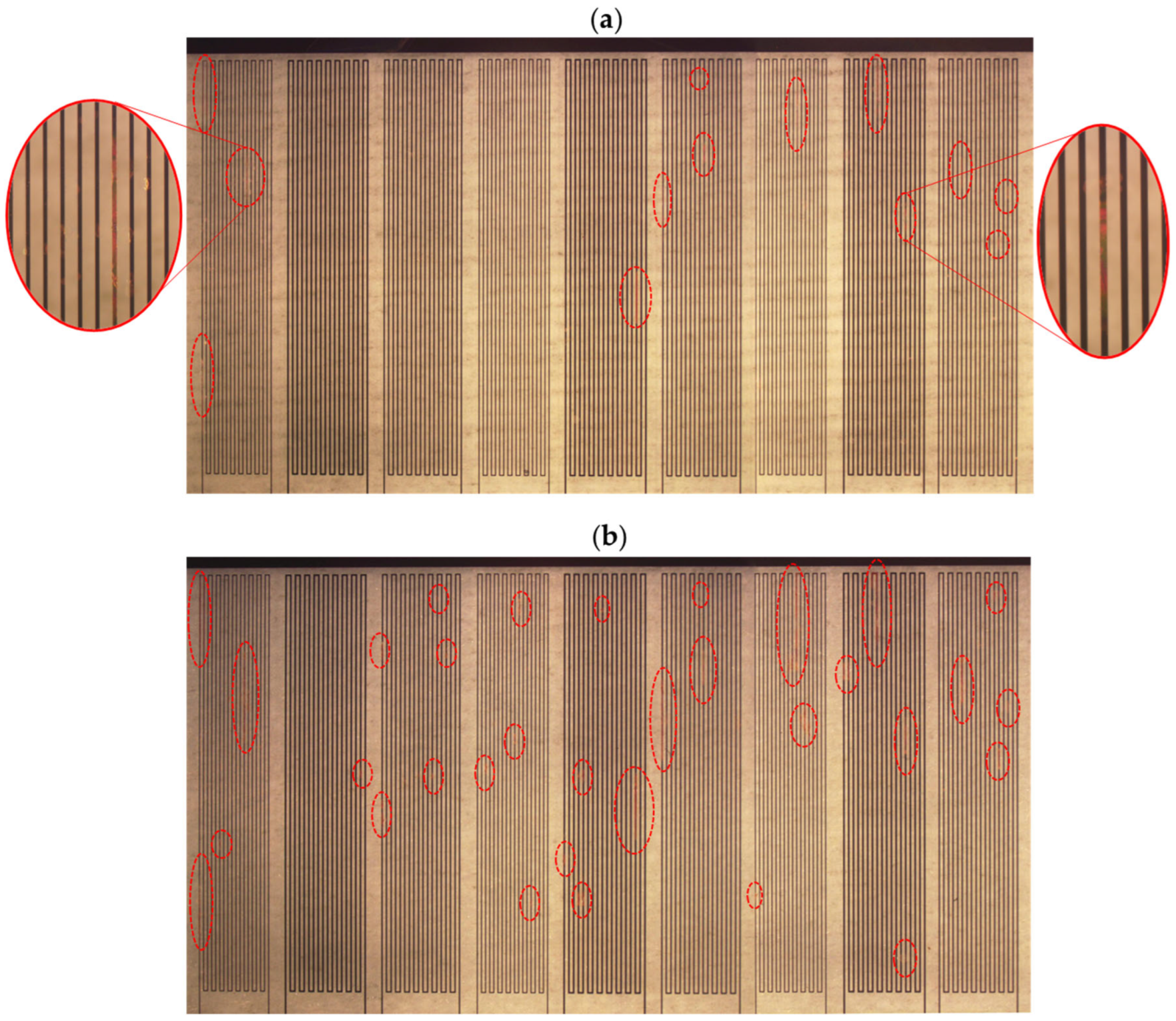
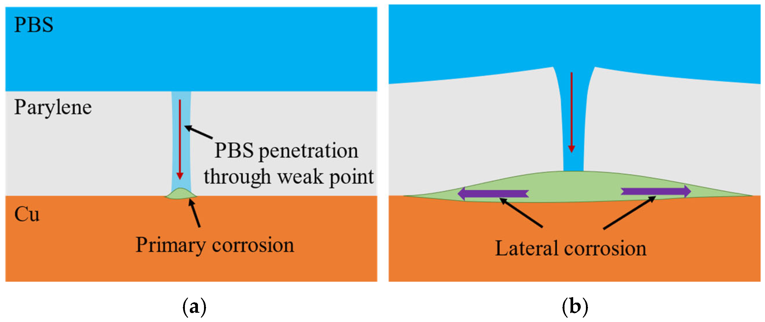
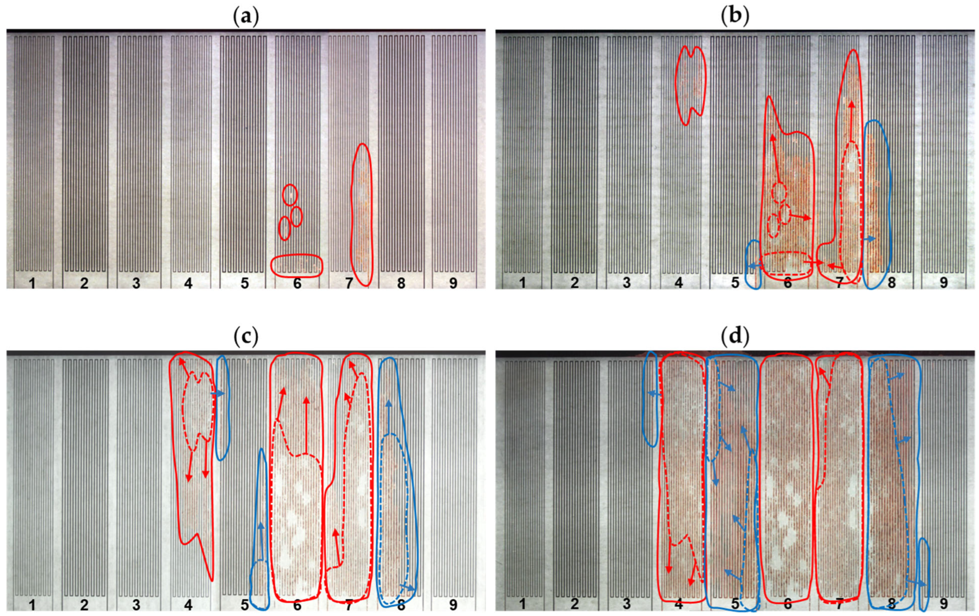
3.1. Pinhole Test
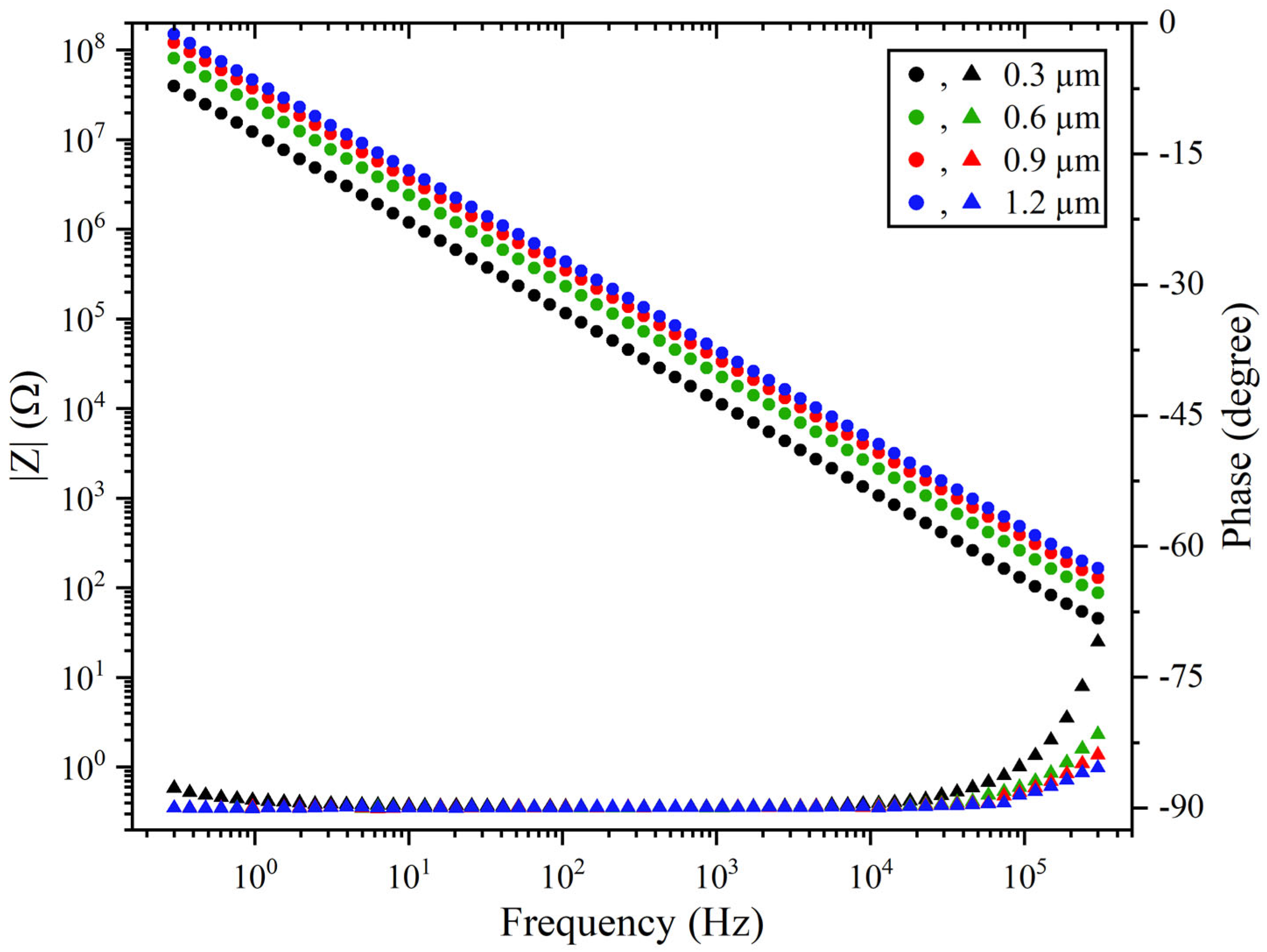
3.2. EIS Results
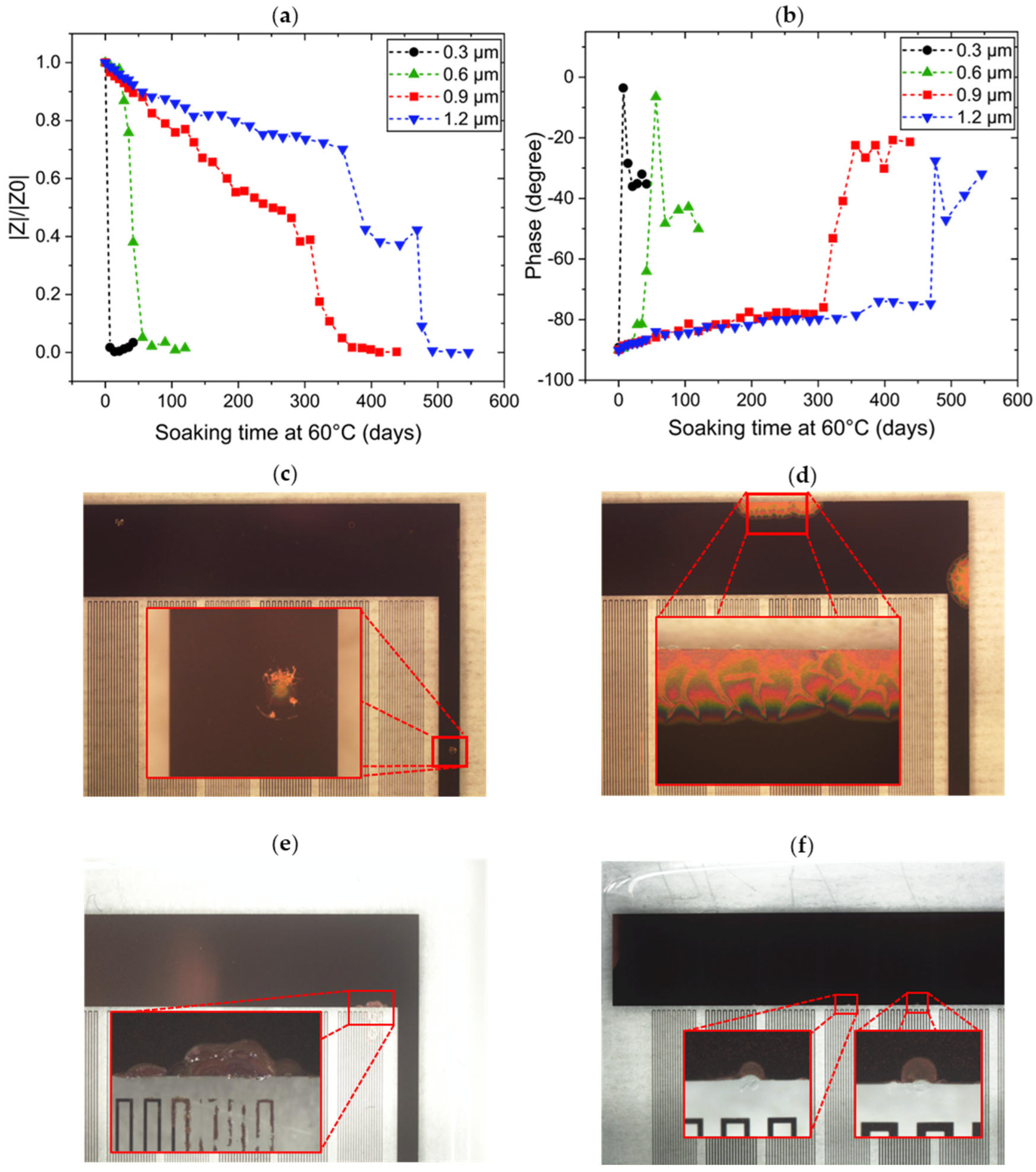
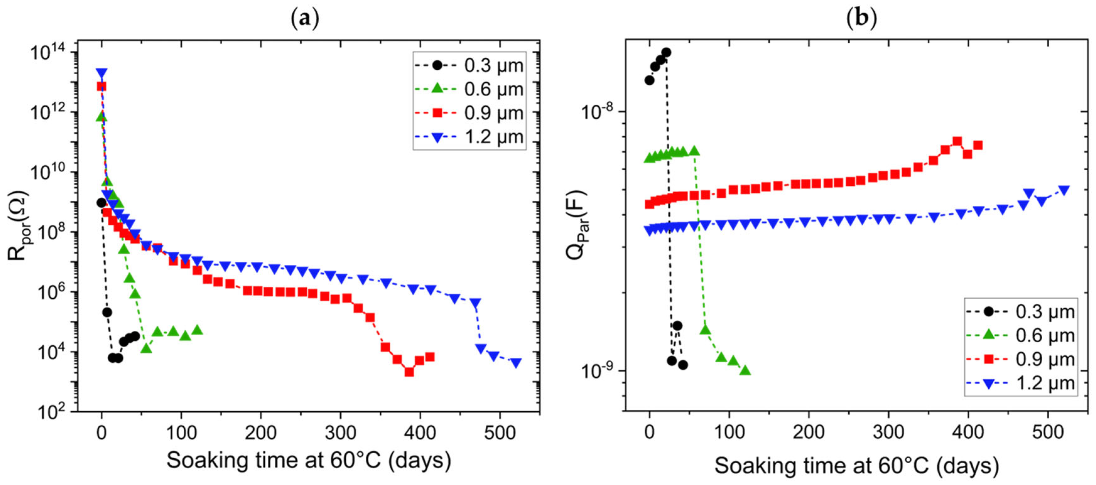
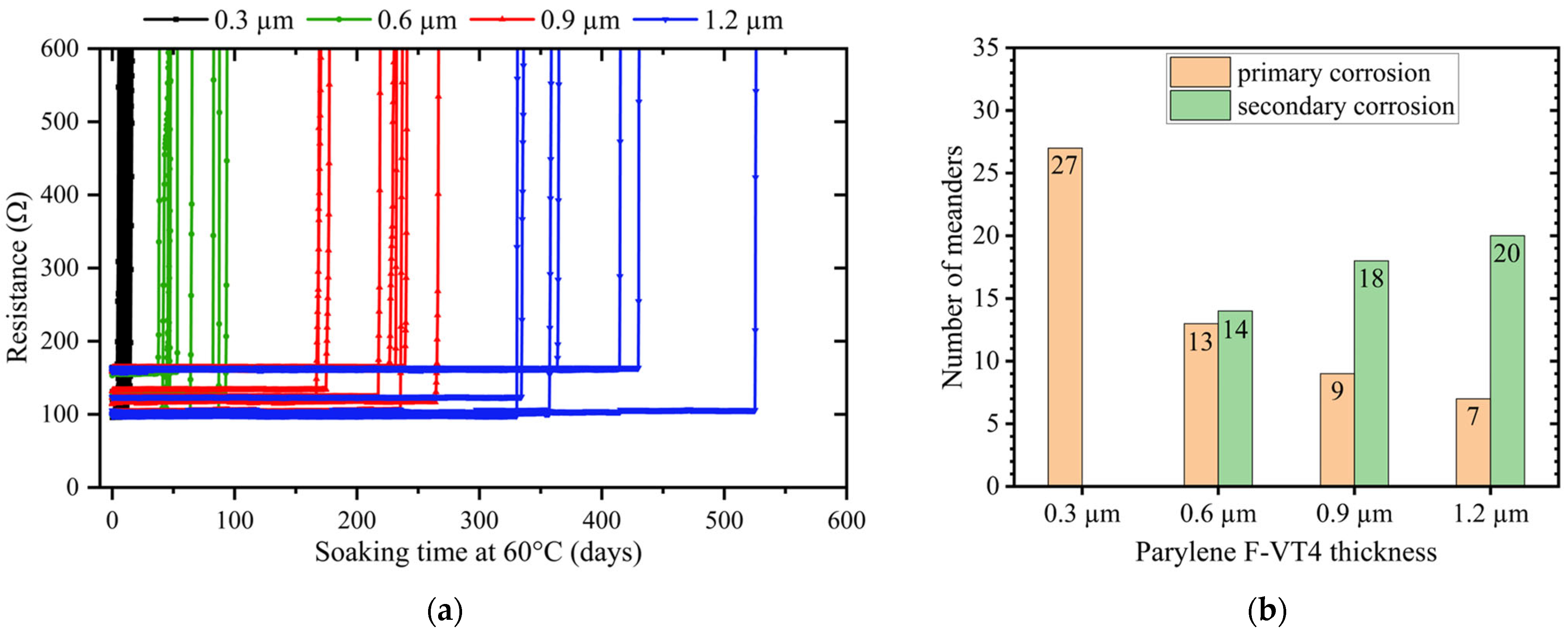
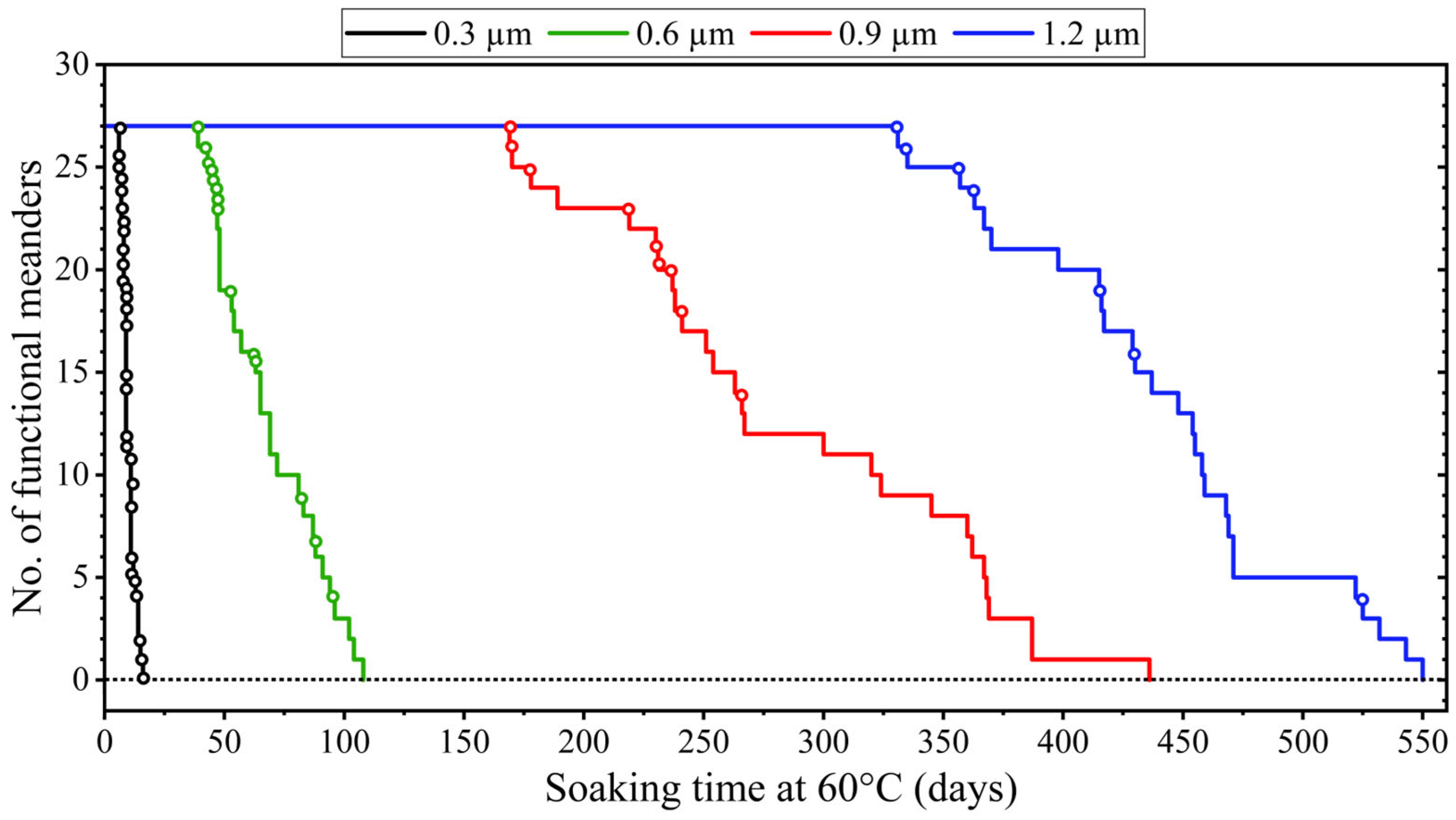
3.3. Resistance-Based Lifetime Testing
3.4. Mean Time to Failure and Lifetime
4. Conclusions
Author Contributions
Funding
Institutional Review Board Statement
Informed Consent Statement
Data Availability Statement
Acknowledgments
Conflicts of Interest
References
- Khan, W.; Muntimadugu, E.; Jaffe, M.; Domb, A.J. Implantable Medical Devices. In Focal Controlled Drug Deliver; Springer: Boston, MA, USA, 2014; pp. 33–59. [Google Scholar]
- Bazaka, K.; Jacob, M.V. Implantable Devices: Issues and Challenges. Electronics 2012, 2, 1–34. [Google Scholar] [CrossRef]
- Cho, Y.U.; Lim, S.L.; Hong, J.-H.; Yu, K.J. Transparent Neural Implantable Devices: A Comprehensive Review of Challenges and Progress. npj Flex. Electron. 2022, 6, 53. [Google Scholar] [CrossRef]
- Sang, M.; Kim, K.; Shin, J.; Yu, K.J. Ultra-thin Flexible Encapsulating Materials for Soft Bio-integrated Electronics. Adv. Sci. 2022, 9, 2202980. [Google Scholar] [CrossRef] [PubMed]
- Mariello, M.; Kim, K.; Wu, K.; Lacour, S.P.; Leterrier, Y. Recent Advances in Encapsulation of Flexible Bioelectronic Implants: Materials, Technologies, and Characterization Methods. Adv. Mater. 2022, 34, 2201129. [Google Scholar] [CrossRef]
- Ahn, S.-H.; Jeong, J.; Kim, S.J. Emerging Encapsulation Technologies for Long-Term Reliability of Microfabricated Implantable Devices. Micromachines 2019, 10, 508. [Google Scholar] [CrossRef]
- Kim, S.H.; Moon, J.-H.; Kim, J.H.; Jeong, S.M.; Lee, S.-H. Flexible, Stretchable and Implantable PDMS Encapsulated Cable for Implantable Medical Device. Biomed. Eng. Lett. 2011, 1, 199–203. [Google Scholar] [CrossRef]
- Hsu, J.-M.; Rieth, L.; Normann, R.A.; Tathireddy, P.; Solzbacher, F. Encapsulation of an Integrated Neural Interface Device with Parylene C. IEEE Trans. Biomed. Eng. 2008, 56, 23–29. [Google Scholar] [CrossRef]
- Caldwell, R.; Street, M.G.; Sharma, R.; Takmakov, P.; Baker, B.; Rieth, L. Characterization of Parylene-C Degradation Mechanisms: In Vitro Reactive Accelerated Aging Model Compared to Multiyear In Vivo Implantation. Biomaterials 2020, 232, 119731. [Google Scholar] [CrossRef]
- Golda-Cepa, M.; Engvall, K.; Hakkarainen, M.; Kotarba, A. Recent Progress on Parylene C Polymer for Biomedical Applications: A Review. Prog. Org. Coat. 2020, 140, 105493. [Google Scholar] [CrossRef]
- Vaeth, K.M.; Jensen, K.F. Transition Metals for Selective Chemical Vapor Deposition of Parylene-Based Polymers. Chem. Mater. 2000, 12, 1305–1313. [Google Scholar] [CrossRef]
- Kahouli, A.; Sylvestre, A.; Laithier, J.-F.; Lutsen, L.; Pairis, S.; André, E.; Garden, J.-L. Structural and Dielectric Properties of Parylene-VT4 Thin Films. Mater. Chem. Phys. 2014, 143, 908–914. [Google Scholar] [CrossRef]
- Buchwalder, S.; Borzì, A.; Diaz Leon, J.J.; Bourgeois, F.; Nicolier, C.; Nicolay, S.; Neels, A.; Zywitzki, O.; Hogg, A.; Burger, J. Thermal Analysis of Parylene Thin Films for Barrier Layer Applications. Polymers 2022, 14, 3677. [Google Scholar] [CrossRef] [PubMed]
- Tipnis, N.P.; Burgess, D.J. Sterilization of Implantable Polymer-Based Medical Devices: A Review. Int. J. Pharm. 2018, 544, 455–460. [Google Scholar] [CrossRef] [PubMed]
- Li, C.; Cauwe, M.; Yang, Y.; Schaubroeck, D.; Mader, L.; Op de Beeck, M. Ultra-Long-Term Reliable Encapsulation Using an Atomic Layer Deposited HfO2/Al2O3/HfO2 Triple-Interlayer for Biomedical Implants. Coatings 2019, 9, 579. [Google Scholar] [CrossRef]
- Li, C.M.; Dong, H.; Cao, X.; Luong, J.H.; Zhang, X. Implantable Electrochemical Sensors for Biomedical and Clinical Applications: Progress, Problems, and Future Possibilities. Curr. Med. Chem. 2007, 14, 937–951. [Google Scholar]
- Baxter, L.K. Capacitive Sensors: Design and Applications; IEEE: New York, NY, USA, 1997. [Google Scholar]
- Daniels, J.S.; Pourmand, N. Label-free Impedance Biosensors: Opportunities and Challenges. Electroanal. Int. J. Devoted Fundam. Pract. Asp. Electroanal. 2007, 19, 1239–1257. [Google Scholar] [CrossRef]
- Oevermann, J.; Weber, P.; Tretbar, S.H. Encapsulation of Capacitive Micromachined Ultrasonic Transducers (CMUTs) for the Acoustic Communication between Medical Implants. Sensors 2021, 21, 421. [Google Scholar] [CrossRef]
- Yaacob, M.I.H.; Arshad, M.R.; Manaf, A.A.; Rahman, M.F.A.; Samsuri, S.S. Enhancement of Piezoelectric Micromachined Ultrasonic Transducer Using Polymer Membrane for Underwater Applications. Indian J. Mar. Sci. 2012, 41, 533–539. [Google Scholar]
- Grundmeier, G.; Schmidt, W.; Stratmann, M. Corrosion Protection by Organic Coatings: Electrochemical Mechanism and Novel Methods of Investigation. Electrochim. Acta 2000, 45, 2515–2533. [Google Scholar] [CrossRef]
- Deflorian, F.; Rossi, S. An EIS Study of Ion Diffusion through Organic Coatings. Electrochim. Acta 2006, 51, 1736–1744. [Google Scholar] [CrossRef]
- Castela, A.S.L.; Simoes, A.M.; Ferreira, M.G.S. EIS Evaluation of Attached and Free Polymer Films. Prog. Org. Coat. 2000, 38, 1–7. [Google Scholar] [CrossRef]
- Lyon, S.B.; Bingham, R.; Mills, D.J. Advances in Corrosion Protection by Organic Coatings: What We Know and What We Would like to Know. Prog. Org. Coat. 2017, 102, 2–7. [Google Scholar] [CrossRef]
- Zhang, Y.; Bertrand, J.A.; Yang, R.; George, S.M.; Lee, Y.C. Electroplating to Visualize Defects in Al2O3 Thin Films Grown Using Atomic Layer Deposition. Thin Solid Film. 2009, 517, 3269–3272. [Google Scholar] [CrossRef]
- Vanhaverbeke, C.; Cauwe, M.; Stockman, A.; de Beeck, M.O.; De Smet, H. Comparison of Copper Electroplating, Copper Wet Etching and Linear Sweep Voltammetry as Techniques to Investigate the Porosity of Atomic Layer Deposited Al2O3. Thin Solid Film. 2019, 686, 137424. [Google Scholar] [CrossRef]
- Li, C.; Cauwe, M.; Mader, L.; Schaubroeck, D.; Op de Beeck, M. Accelerated Hermeticity Testing of Biocompatible Moisture Barriers Used for the Encapsulation of Implantable Medical Devices. Coatings 2019, 10, 19. [Google Scholar] [CrossRef]
- Hukins, D.W.L.; Mahomed, A.; Kukureka, S.N. Accelerated Aging for Testing Polymeric Biomaterials and Medical Devices. Med. Eng. Phys. 2008, 30, 1270–1274. [Google Scholar] [CrossRef]
- Hemmerich, K.J. General Aging Theory and Simplified Protocol for Accelerated Aging of Medical Devices. Med. Plast. Biomater. 1998, 5, 16–23. [Google Scholar]
- Loveday, D.; Peterson, P.; Rodgers, B. Evaluation of Organic Coatings with Electrochemical Impedance Spectroscopy. JCT Coat. Tech. 2004, 8, 46–52. [Google Scholar]
- Van Westing, E.P.M.; Ferrari, G.M.; De Wit, J.H.W. The Determination of Coating Performance Using Electrochemical Impedance Spectroscopy. Electrochim. Acta 1994, 39, 899–910. [Google Scholar] [CrossRef]
- Fernández-Sánchez, C.; McNeil, C.J.; Rawson, K. Electrochemical Impedance Spectroscopy Studies of Polymer Degradation: Application to Biosensor Development. TrAC Trends Anal. Chem. 2005, 24, 37–48. [Google Scholar] [CrossRef]
- González-Hernández, A.; Morales-Cepeda, A.B.; Flores, M.; Caicedo, J.C.; Aperador, W.; Amaya, C. Electrochemical Properties of TiWN/TiWC Multilayer Coatings Deposited by RF-Magnetron Sputtering on AISI 1060. Coatings 2021, 11, 797. [Google Scholar] [CrossRef]
- Chun, W.; Chou, N.; Cho, S.; Yang, S.; Kim, S. Evaluation of Sub-Micrometer Parylene C Films as an Insulation Layer Using Electrochemical Impedance Spectroscopy. Prog. Org. Coat. 2014, 77, 537–547. [Google Scholar] [CrossRef]
- Brasher, D.M.; Kingsbury, A.H. Electrical Measurements in the Study of Immersed Paint Coatings on Metal. I. Comparison between Capacitance and Gravimetric Methods of Estimating Water-uptake. J. Appl. Chem. 1954, 4, 62–72. [Google Scholar] [CrossRef]
- Minnikanti, S.; Diao, G.; Pancrazio, J.J.; Xie, X.; Rieth, L.; Solzbacher, F.; Peixoto, N. Lifetime Assessment of Atomic-Layer-Deposited Al2O3–Parylene C Bilayer Coating for Neural Interfaces Using Accelerated Age Testing and Electrochemical Characterization. Acta Biomater. 2014, 10, 960–967. [Google Scholar] [CrossRef]
- Mengesha, G.A.; Chu, J.P.; Lou, B.-S.; Lee, J.-W. Corrosion Performance of Plasma Electrolytic Oxidation Grown Oxide Coating on Pure Aluminum: Effect of Borax Concentration. J. Mater. Res. Technol. 2020, 9, 8766–8779. [Google Scholar] [CrossRef]
- Gao, Z.; Jiang, Y.; Meng, Y.; Du, M.; Liu, F. A Review of the Fabrication of Pinhole-Free Thin Films Based on Electrodeposition Technology: Theory, Methods and Progress. Molecules 2024, 29, 5615. [Google Scholar] [CrossRef]
- Panjan, P.; Drnovšek, A.; Gselman, P.; Čekada, M.; Panjan, M. Review of Growth Defects in Thin Films Prepared by PVD Techniques. Coatings 2020, 10, 447. [Google Scholar] [CrossRef]
- Camacho-Espinosa, E.; Oliva-Avilés, A.I.; Oliva, A.I. Effect of the Substrate Cleaning Process on Pinhole Formation in Sputtered CdTe Films. J. Mater. Eng. Perform. 2017, 26, 4020–4028. [Google Scholar] [CrossRef]
- Trentin, A.; Pakseresht, A.; Duran, A.; Castro, Y.; Galusek, D. Electrochemical Characterization of Polymeric Coatings for Corrosion Protection: A Review of Advances and Perspectives. Polymers 2022, 14, 2306. [Google Scholar] [CrossRef]
- Margarit-Mattos, I.C.P. EIS and Organic Coatings Performance: Revisiting Some Key Points. Electrochim. Acta 2020, 354, 136725. [Google Scholar] [CrossRef]
- Pokhodnya, K.I.; Bonner, M.; Miller, J.S. Parylene Protection Coatings for Thin Film V [TCNE]x Room Temperature Magnets. Chem. Mater. 2004, 16, 5114–5119. [Google Scholar] [CrossRef]
- Nguyen, A.S.; Causse, N.; Musiani, M.; Orazem, M.E.; Pébère, N.; Tribollet, B.; Vivier, V. Determination of Water Uptake in Organic Coatings Deposited on 2024 Aluminium Alloy: Comparison Between Impedance Measurements and Gravimetry. Prog. Org. Coat. 2017, 112, 93–100. [Google Scholar] [CrossRef]
- Madelat, N.; Wouters, B.; Jalilian, E.; Van Assche, G.; Hubin, A.; Terryn, H.; Hauffman, T. Differentiating between the Diffusion of Water and Ions from Aqueous Electrolytes in Organic Coatings Using an Integrated Spectro-Electrochemical Technique. Corros. Sci. 2023, 212, 110919. [Google Scholar] [CrossRef]
- Petrunin, M.A.; Maksaeva, L.B.; Gladkikh, N.A.; Yurasova, T.A.; Maleeva, M.A.; Ignatenko, V.E. Cathodic Delamination of Polymer Coatings from Metals. Mechanism and Prevention Methods. A Review. Int. J. Corros. Scale Inhib. 2021, 10, 1–28. [Google Scholar]
- Leidheiser, H., Jr.; Wang, W.; Igetoft, L. The Mechanism for the Cathodic Delamination of Organic Coatings from a Metal Surface. Prog. Org. Coat. 1983, 11, 19–40. [Google Scholar] [CrossRef]


| Parylene F-VT4 Thickness | Pinhole Count (10 min) | Pinhole Count (20 min) | Pinhole Count (30 min) |
| 0.3 µm | 37 ± 3 | 42 ± 5 | 42 ± 5 |
| 0.6 µm | 3 ± 1 | 6 ± 2 | 6 ± 2 |
| 0.9 µm | 0 | 0 | 0 |
| 1.2 µm | 0 | 0 | 0 |
| Parylene F-VT4 Thickness | Extracted CPar (nF) | Theoretical CPar (nF) |
|---|---|---|
| 0.3 µm | 13.21 | 13.14 |
| 0.6 µm | 6.55 | 6.65 |
| 0.9 µm | 4.39 | 4.41 |
| 1.2 µm | 3.50 | 3.45 |
| Parylene F-VT4 Thickness | MTTF at 60 °C (Days) Mean ± σ | Extrapolated MTTF at 37 °C (Q10 = 2) |
| 0.3 µm | 9.4 ± 2.8 | ~1.5 months |
| 0.6 µm | 57 ± 18.6 | ~9.5 months |
| 0.9 µm | 215.4 ± 34.8 | ~3 years |
| 1.2 µm | 393.7 ± 69 | ~5.5 years |
| Parylene F-VT4 Thickness | Lifetime at 60 °C (Days) | Extrapolated Lifetime at 37 °C (Q10 = 2) |
| 0.3 µm | 5 | ~25 days |
| 0.6 µm | 38 | ~6.4 months |
| 0.9 µm | 169 | ~2.3 years |
| 1.2 µm | 331 | ~4.5 years |
Disclaimer/Publisher’s Note: The statements, opinions and data contained in all publications are solely those of the individual author(s) and contributor(s) and not of MDPI and/or the editor(s). MDPI and/or the editor(s) disclaim responsibility for any injury to people or property resulting from any ideas, methods, instructions or products referred to in the content. |
© 2025 by the authors. Licensee MDPI, Basel, Switzerland. This article is an open access article distributed under the terms and conditions of the Creative Commons Attribution (CC BY) license (https://creativecommons.org/licenses/by/4.0/).
Share and Cite
Afshari, E.; Verplancke, R.; Cauwe, M.; Op de Beeck, M. Quality and Lifetime of Thin Parylene F-VT4 Coatings for Hermetic Encapsulation of Implantable Medical Devices. Coatings 2025, 15, 648. https://doi.org/10.3390/coatings15060648
Afshari E, Verplancke R, Cauwe M, Op de Beeck M. Quality and Lifetime of Thin Parylene F-VT4 Coatings for Hermetic Encapsulation of Implantable Medical Devices. Coatings. 2025; 15(6):648. https://doi.org/10.3390/coatings15060648
Chicago/Turabian StyleAfshari, Esmaeil, Rik Verplancke, Maarten Cauwe, and Maaike Op de Beeck. 2025. "Quality and Lifetime of Thin Parylene F-VT4 Coatings for Hermetic Encapsulation of Implantable Medical Devices" Coatings 15, no. 6: 648. https://doi.org/10.3390/coatings15060648
APA StyleAfshari, E., Verplancke, R., Cauwe, M., & Op de Beeck, M. (2025). Quality and Lifetime of Thin Parylene F-VT4 Coatings for Hermetic Encapsulation of Implantable Medical Devices. Coatings, 15(6), 648. https://doi.org/10.3390/coatings15060648