1. Introduction
Silicon carbide (SiC) ceramics, as high-performance inorganic non-metallic materials, have attracted significant attention due to their excellent mechanical properties, thermal stability [
1], and chemical inertness [
2]. They have been extensively applied in both traditional and emerging energy sectors [
3] and the automotive coatings industry [
4]. However, with the continuous expansion of the international semiconductor market in recent years, the demand for materials that can be processed into various SiC electronic devices via electrical discharge machining (EDM) has also increased, bringing conductive SiC ceramics into the spotlight [
5]. In recent years, we have seen a gradual increase in reports on novel applications of SiC-based devices in sensors [
6] and thermoelectric converters [
7]. The widespread adoption of chemical vapor deposition SiC (CVD-SiC) in semiconductor manufacturing—particularly for plasma etching chambers, ion implantation fixtures, and electrostatic dissipation components—stems from its precise electrical resistivity control. However, the prohibitive production costs associated with CVD-SiC (estimated to be 3–5 times higher than conventional methods) have driven substantial research efforts to develop cost-effective alternatives [
8]. Recent studies suggest that hot-pressed SiC (HP-SiC), with optimized dopant concentrations during sintering, demonstrates a comparable electrical performance at significantly reduced fabrication expenses [
8]. Kim reported on the factors affecting liquid-phase-sintered silicon carbide (LPS-SiC) and successfully prepared conductive SiC ceramics using hot-press sintering, achieving a resistivity ranging between 3.5 × 10
−3 and 3 × 10
13 Ω·cm [
9]. Qing-Qing Shao, Ting-Ting Zhao et al. reported the observation of stacking faults and core–rim structures in silicon carbide (SiC), which affect the material’s properties [
10,
11]. Kim et al. also discovered through EDS analysis that by introducing N into SiC grains or adding a conductive secondary phase, SiC powders with resistivity in the range of 1000–100 Ω·cm can be sintered to form ceramics with resistivity reduced to 0.1–0.001 Ω·cm. The electrical conductivity of SiC ceramics has been significantly enhanced [
12,
13,
14].
However, due to the large energy bandgap of SiC (for example, the energy bandgaps of the 3C, 6H, and 4H polytypes are 2.4 eV, 3.0 eV, and 3.3 eV, respectively, at room temperature), the intrinsic resistivity of SiC is relatively high compared to that of single-crystal or polycrystalline silicon [
15]. Additionally, introducing nitrogen (N) atoms into SiC to substitute for carbon (C) atoms in order to reduce its resistivity is challenging due to the low diffusivity of N atoms in SiC [
16].
Among the multiple examples of successfully achieving nitrogen doping to produce conductive SiC ceramics, using yttrium nitrate tetrahydrate Y(NO
3)
3·4H
2O as a sintering additive during hot-press sintering effectively reduced the electrical resistivity of the resulting 3C-SiC ceramics to 10
−3 Ω·cm at room temperature [
17]. This finding, along with the results from electron probe microanalysis (EPMA), suggests that the YN-sintered SiC samples achieved effective N doping. The nitrogen atoms substitute for carbon sites in the 3C-SiC lattice (zinc blende structure), thereby creating donor levels near the conduction band [
18]. This substitution facilitates easier electron transitions, consequently reducing the resistivity. In the previously mentioned YN-sintered SiC samples, the Y
2O
3 phase present at the grain boundaries transforms into an amorphous Y-Si oxycarbonitride glass phase during hot-press sintering conducted in nitrogen atmosphere. This transformation is achieved through a dissolution and reprecipitation mechanism, which aids in the densification of SiC [
9]. At the same time, under the effects of temperature and pressure, some nitrogen atoms migrate from the grain boundaries into the SiC grains with the assistance of yttrium. This incorporation of nitrogen into the SiC lattice achieves effective YN doping, leading to a reduction in the resistivity of the SiC samples.
However, the above reports did not investigate from a more microscopic perspective regarding how much of the Y and N elements entered into the SiC grains, how they were distributed within the grains, or whether the phase formed at the grain boundaries was indeed a glassy phase.
In this study, compared to conventional sintering methods, the strategy of YN doping to improve the electrical conductivity of SiC was adopted for innovative low-temperature secondary heat treatment, which effectively reduced their resistivity. To better facilitate nitrogen’s entry from the grain boundaries into the SiC lattice for substituting carbon atoms and to retain more of the 3C-SiC structure, SiC samples doped with Y2O3 and graphite were fabricated via low-temperature hot-press sintering. Subsequently, these samples underwent a secondary nitriding treatment at different temperatures. Following the treatment, scanning electron microscopy (SEM) and transmission electron microscopy (TEM), coupled with analytical techniques, revealed the distribution of Y and N elements within the SiC grains and nitridation regions, further elucidating their compositional content and phase constitution.
2. Experimental Procedure
In order to prepare SiC containing graphite and trace amounts of Al, N and Y, micron-sized β-SiC (Xi’an BOERNM New Materials Co., Ltd., Xi’an, China, average particle size 0.5 µm), nano-sized β-SiC (Xi’an BOERNM New Materials Co., Ltd., Xi’an, China, average particle size 50 nm), graphite (Beijing Yinuokai Chemical Co., Ltd., Beijing, China, purity ≥ 99.999%), AlN (Beijing Yinuokai Chemical Co., Ltd., Beijing, China, N ≥ 32%), and Y
2O
3 (Shanghai Diyang Chemical Co., Ltd., Shanghai, China, purity ≥ 99.999%) were prepared. They were mixed in a weight ratio of 90:8:1:0.5:0.5 (0.5 µmSiC:50 nmSiC:graphite:AlN:Y
2O
3). The mixture was treated by high-speed ball milling in ethanol for 12 h in a polypropylene jar using SiC media. The incorporation of a small amount of nanoscale SiC powder enhances the milling activity during ball milling, promoting a more uniform dispersion of the SiC powder matrix. The addition of AlN was intended to fully utilize the mechanism of liquid-phase sintering [
12], enabling SiC to achieve maximum densification at a lower temperature, while the incorporation of small amounts of AlN and Y
2O
3 aimed to fabricate SiC ceramics with high purity and density, minimizing the increase in electrical resistivity [
19]. The incorporation of graphite facilitates subsequent nitrogen substitution for carbon during secondary processing, enabling the introduction of more nitrogen atoms from grain boundaries into the SiC grains. The mixture was dried, sieved three times (60 mesh), and then uniaxially pressed at 15 MPa. The compact was then heat-treated at 1450 °C for 30 min, followed by hot-pressing under nitrogen atmosphere at 40 MPa for 2 h at 1850 °C to obtain the SAN-C sample.
SAN-C ceramics were further heat-treated in 3 MPa nitrogen atmosphere under 1500 °C, 1650 °C, and 1800 °C for 3 h, respectively, followed by rapid cooling to 950 °C, to prevent nitrogen loss during high-temperature processing. The heat-treated samples are labeled 1500SAN, 1650SAN, and 1800SAN.
The relative densities of the four samples were measured using the Archimedes method, with mercury as the immersion medium. This approach relies on buoyancy principles, where each sample is first weighed in air and then submerged in mercury to determine its apparent mass loss due to displacement. Density was calculated using the following formula:
Relative density is defined as the measured density divided by the theoretical density of the SiC sample (3.21 g/cm
3). The calculation is as follows:
Phase identification and crystal structure analysis were performed using an X-ray powder diffractometer (SmartLab II, Rigaku, Tokyo, Japan) using Cu-Kα1 radiation (λ = 0.154056 nm), and high-resolution diffraction spectra were collected in the range of 20° < 2θ < 80°. The microstructure and morphology of the four samples were observed using SEM (model Gemini 300, Carl Zeiss, Oberkochen, Germany). An elemental analysis of the SAN-C and 1650SAN samples was conducted using EDS (model X-Max, Oxford Instrument, Oxfordshire, UK) at a voltage of 10 kV.
For the measurement of direct current resistivity, the standard four-point probe method was used. The sample dimensions were 10 mm × 3 mm × 3 mm in block form, and a bias current of 1 mA was applied for the measurement. The resistivity of the sample was calculated based on the measured voltage under the bias current. Hall effect measurements were conducted at room temperature using the Van der Pauw technique to determine the carrier mobility of the sample.
3. Result and Discussion
Through hot-pressing treatment at 1850 °C with 40 MPa pressure applied for 2 h, the relative density exceeded 93% (measured relative to the theoretical density of SiC (3.21 g/cm
3)). Specifically, the relative densities of the samples were 93.2% for SAN-C, 98.1% for 1500SAN, 99.2% for 1650SAN, and 99.7% for 1800SAN. The addition of AlN and Y
2O
3 is beneficial for achieving the densification of SiC via liquid-phase sintering. In the SAN-C sample, the combination of AlN-Y
2O
3 additives with graphite enabled densification at lower temperatures [
19].
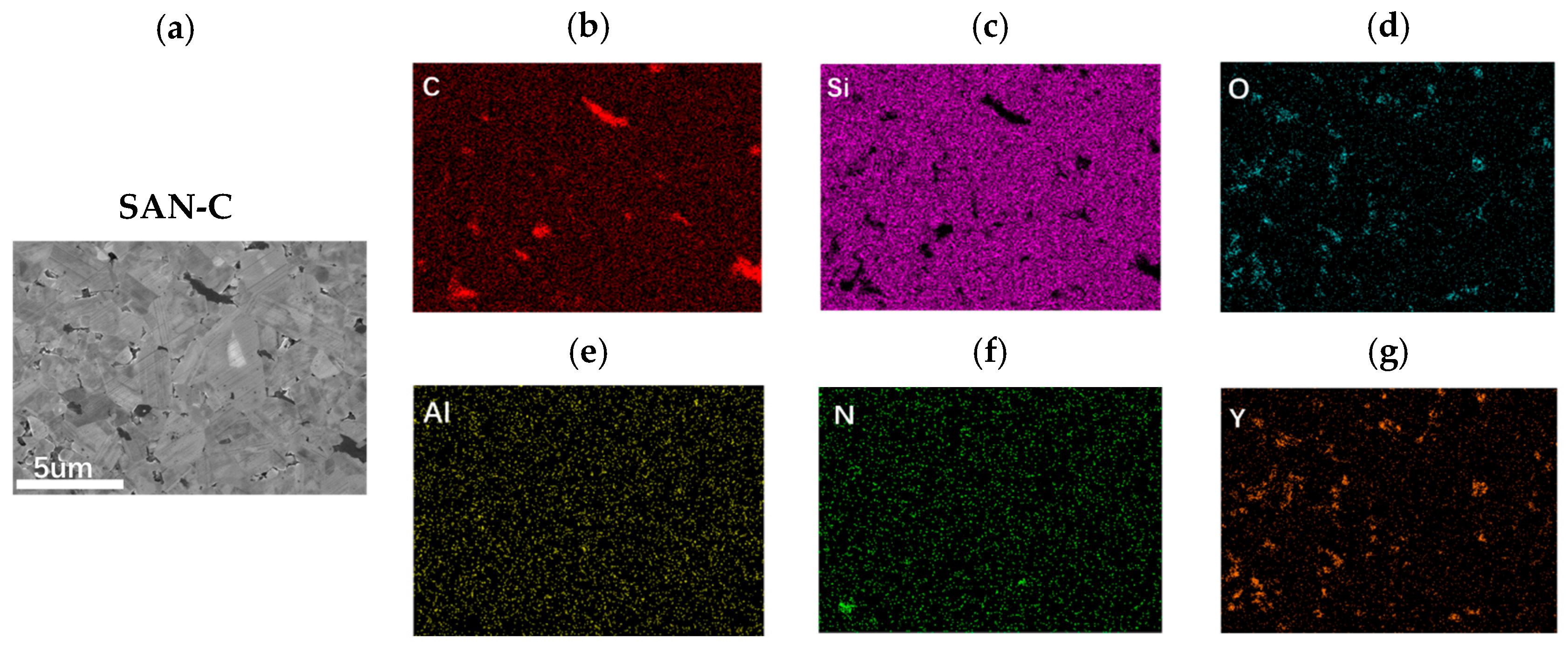
As shown in
Figure 1, SAN-C primarily consists of equiaxed grains with a small fraction of elongated grains, with overall grain sizes ranging from 2 to 4 μm. This indicates the minimal phase transformation of SiC during hot-pressing and limited grain growth due to the relatively low sintering temperature. Some grains exhibit a core–rim structure, likely caused by compositional variations in Al or N within the SiC lattice [
20]. EDS analysis reveals that Y
2O
3 and C predominantly segregate at grain boundaries, forming intergranular secondary phases. The successful incorporation of graphite into the grain boundaries not only enhances the overall electrical conductivity but also facilitates N substitution for C during heat treatment, promoting nitrogen solubility in SiC grains during growth [
19]. Yttrium accumulates at intergranular regions, forming Y-Al-Si amorphous glass phases or remaining as Y
2O
3, which contributes to densification.
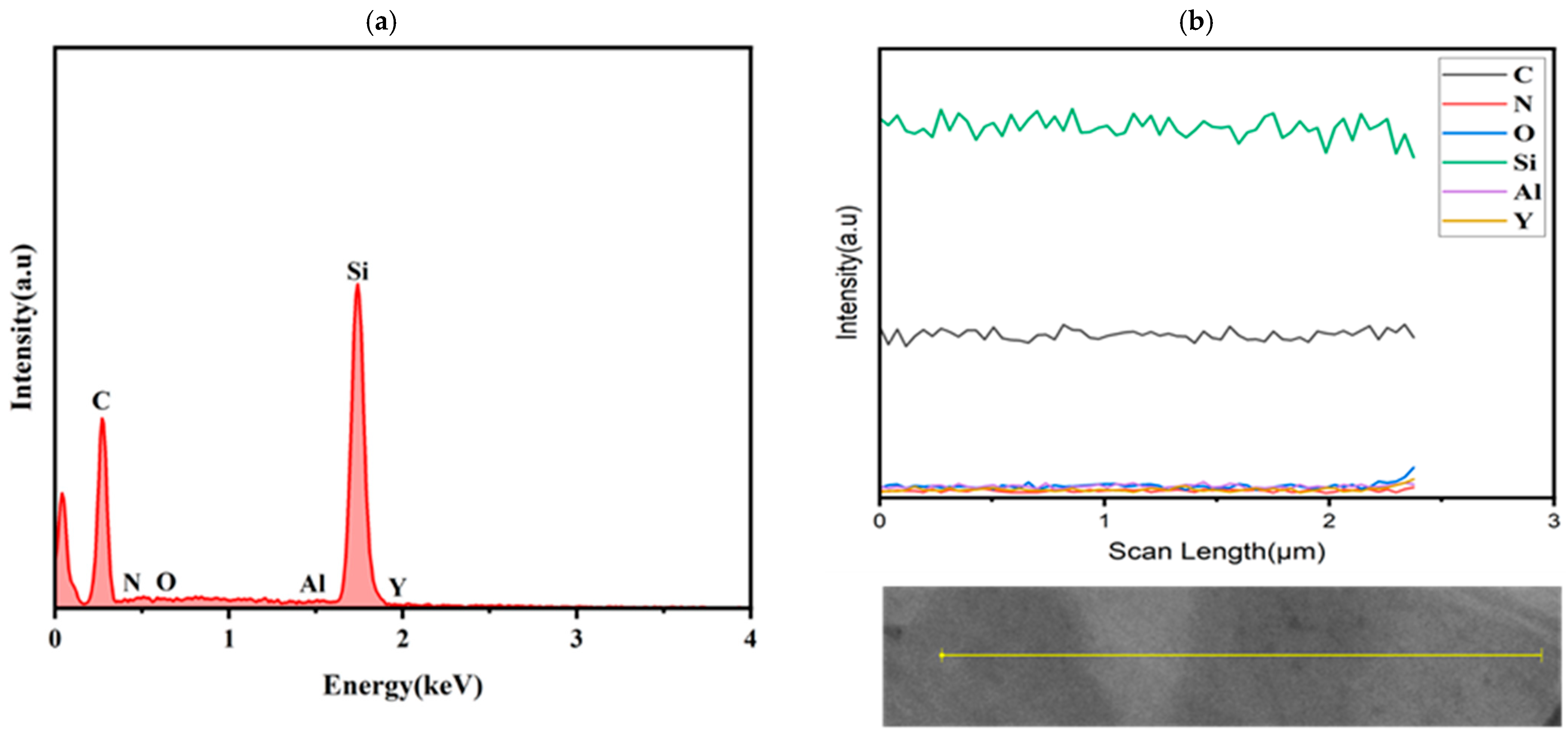
As shown in
Figure 2, the elemental composition distribution within SiC grains is highly uniform. Combined with the quantitative elemental analysis results of SiC grains in the SAN-C sample listed in
Table 1, the low self-diffusion coefficient of nitrogen (N) prevented its incorporation into the SiC grains under the applied sintering conditions. Only trace amounts of Al were dissolved into the SiC grains, leading to the observed core-rim structure. The minimal Al incorporation does not significantly reduce the overall electrical conductivity of the sample. Additionally, the SAN-C sample—characterized by a high proportion of 3C-SiC and high SiC purity—is highly suitable for secondary growth via nitrogen pressure heat treatment.
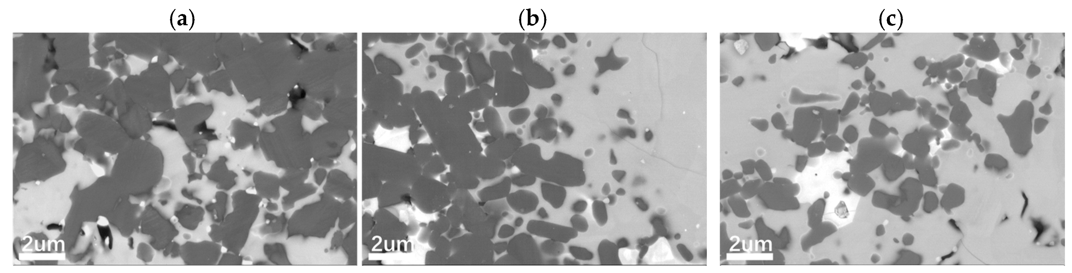
As shown in
Figure 3, the morphology of the samples undergoes significant changes after heat treatment at 1500 °C, 1650 °C, and 1800 °C. BSD (Backscattered Electron Diffraction) analysis reveals that the 1500SAN sample retains equiaxed grains dominated by 3C-SiC, indicating that most of the β-SiC did not undergo a β→α phase transformation under nitrogen pressure. However, compared to the SAN-C sample, the grain size of 1500SAN decreases, with nitrogen-rich regions forming at grain boundaries. These regions contain precipitated Y
2O
3 crystals and residual non-nitrided graphite.
As the temperature increases, the nitrogen-rich regions expand, and SiC grain sizes further decrease. XRD analysis (
Figure 4) confirms the formation of secondary phases in 1650SAN and 1800SAN samples after gas pressure sintering. This is attributed to enhanced nitrogen diffusion and phase segregation at higher temperatures, consistent with the dissolution–reprecipitation mechanism during liquid-phase sintering.
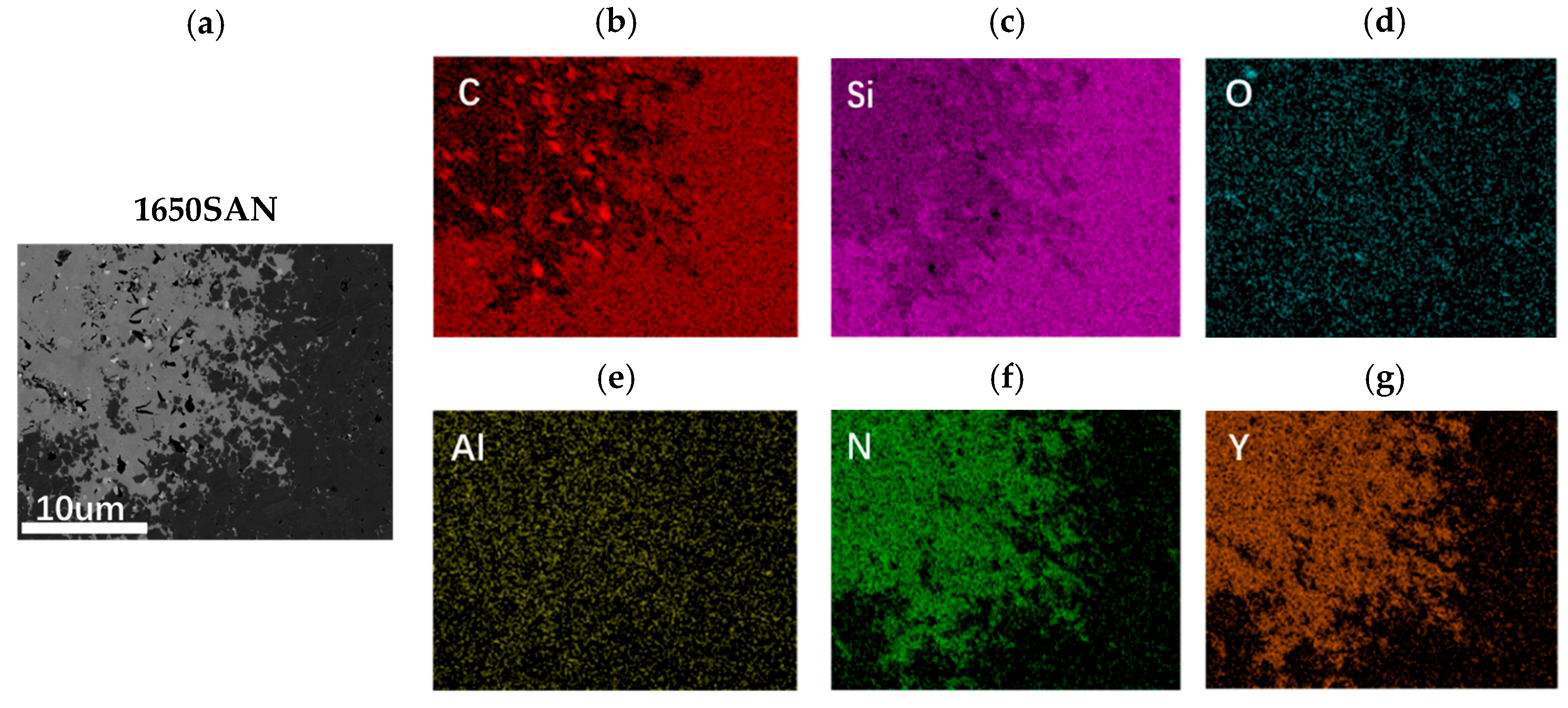
As shown in
Figure 5, an EDS analysis of the 1650SAN sample reveals the enrichment of both N and Y in the nitrogen-rich regions, indicating the potential presence of the Y
2Si
4CN
6 crystalline phase in these areas.
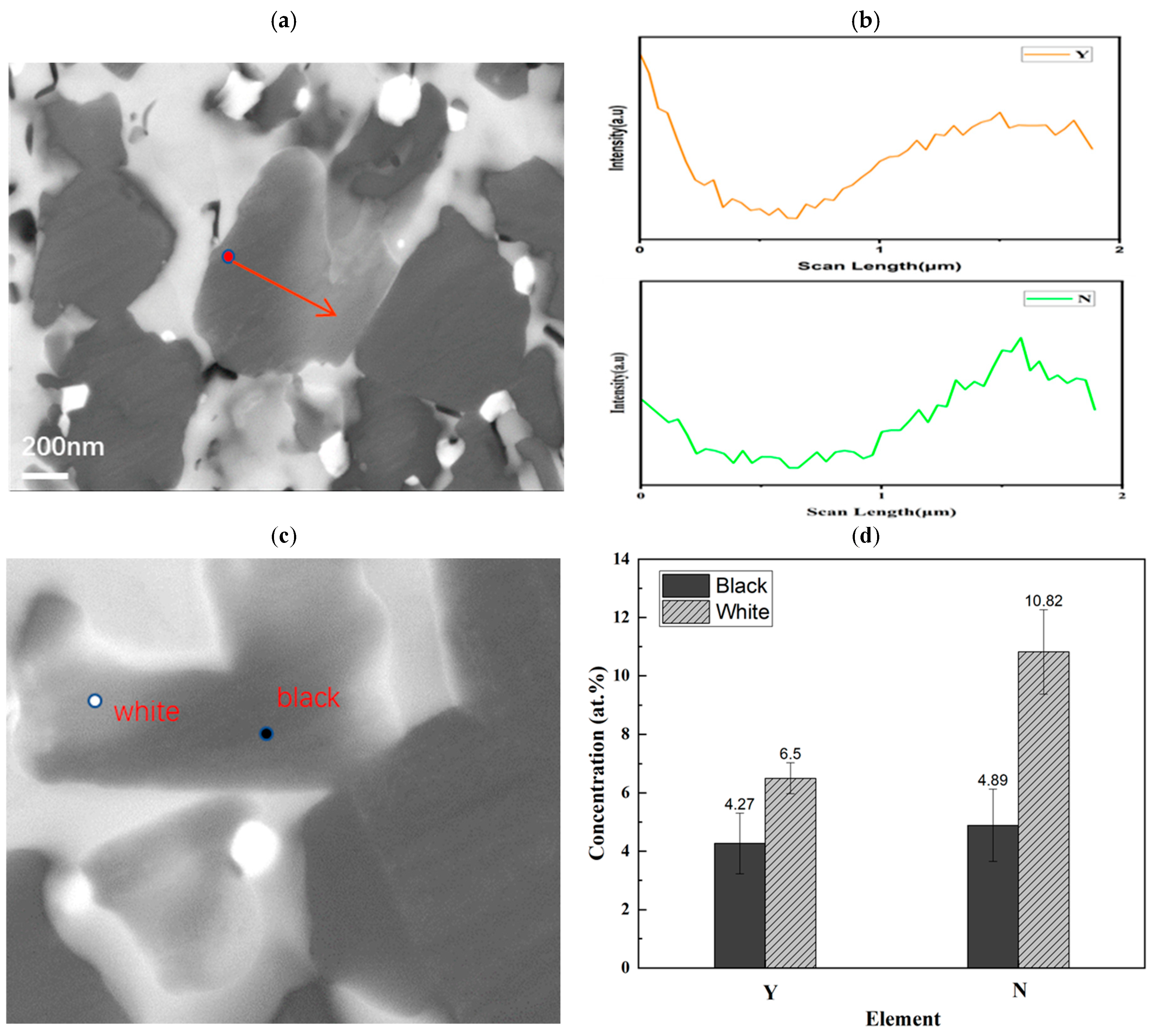
Figure 6 further demonstrates compositional variations within some SiC grains, which manifest as contrast differences in backscattered electron (BSE) signals. By correlating SEM images with EDS line scans, quantitative elemental analysis confirms that Y/N content in bright-contrast areas is much higher than in dark-contrast areas. This suggests that Y/N doping into the SiC lattice under nitrogen pressure enhances the electrical conductivity of the sample.
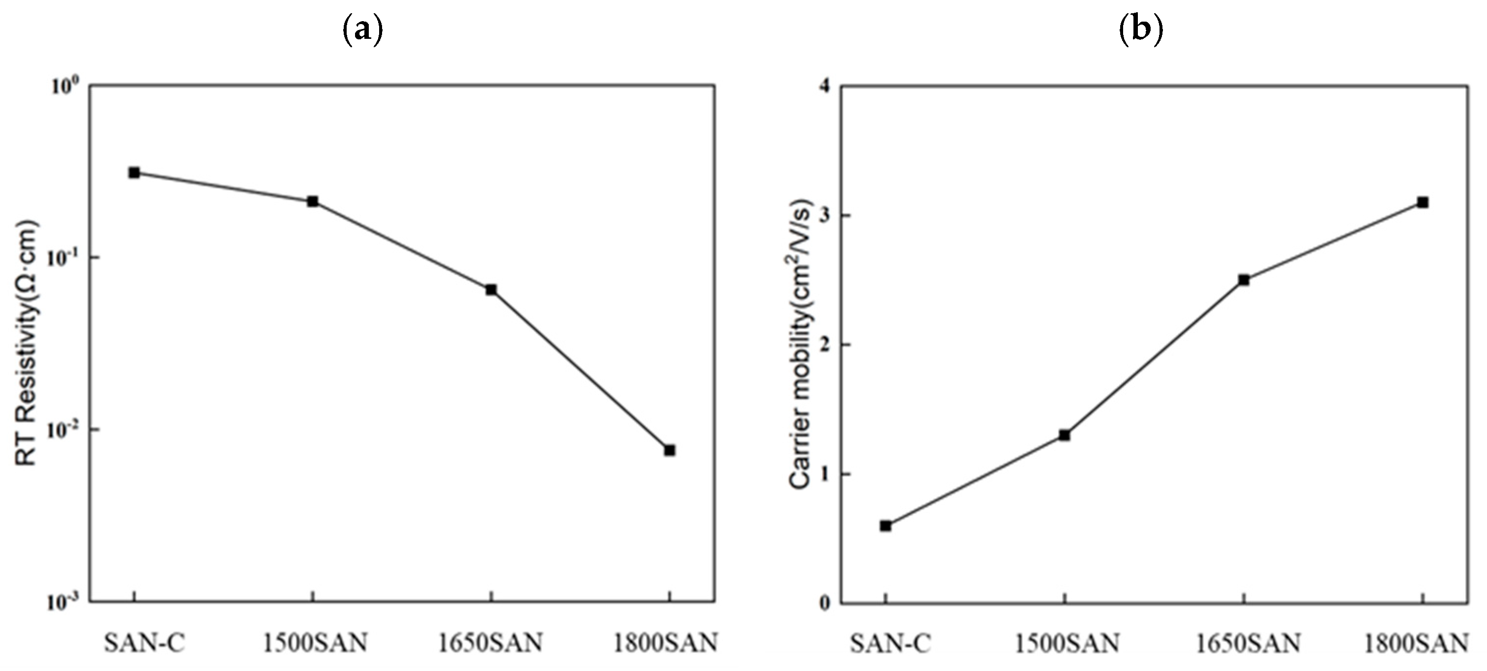
An XRD analysis of the 1650SAN sample revealed additional diffraction peaks beyond those of 3C-SiC and 6H-SiC, consistent with the Y
2Si
4CN
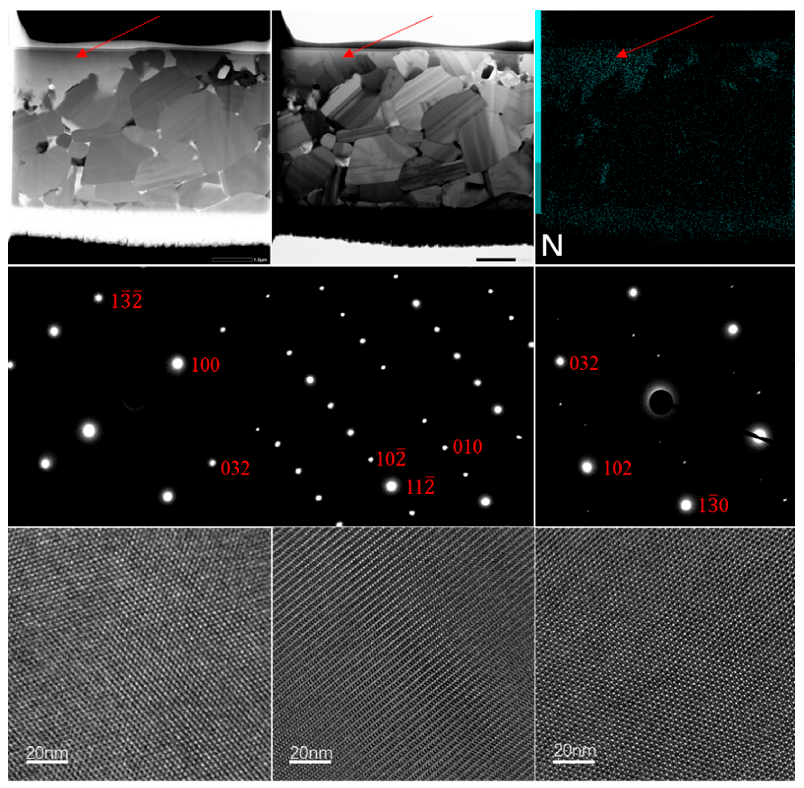
6 phase. A TEM diffraction pattern analysis (
Figure 7) of the nitrogen-rich regions in 1650SAN confirmed the presence of monoclinic Y
2Si
4CN
6 (space group: P2
1/c) through indexing from three crystallographic orientations. Combined with EDS quantitative analysis (
Table 2), the nitrogen-rich regions and contrast variations in SiC grains indicate the formation of YN-doped SiC alongside the Y
2Si
4CN
6 second phase. In contrast, the 1500SAN sample lacked distinct peaks for this phase, while the 1800SAN sample confirmed its presence via morphology, EDS, and XRD analyses. Current research on Y
2Si
4CN
6 is limited, and computational studies indicate that the theoretical band gap of Y
2Si
4CN
6 (3.1 eV) is lower than that of SiC (3.4 eV) [
21]. In addition, under constant nitrogen pressure, the increasing Y
2Si
4CN
6 content with higher annealing temperatures correlates with reduced resistivity (from 2.11 × 10
1 Ω·cm to 7.56 × 10
−3 Ω·cm) and increased carrier mobility (from 1.3 cm
2/(V·s) to 3.1 cm
2/(V·s),
Figure 8,
Table 3). In Y
2Si
4CN
6, nitrogen exists as a substitutional impurity in the -3-oxidation state, and its energy level functions as a donor level, providing electrons to participate in electrical conduction. This suggests that Y
2Si
4CN
6 may replace the non-conductive amorphous phase in the crystal boundary and act as a donor center or form conductive pathways to improve SiC’s electrical conductivity.
Yeongjun Oh et al. [
22] recently fabricated graphite-doped conductive SiC under pressureless conditions and observed that increased graphite doping led to the formation of a conductive network between grains, progressively reducing electrical resistivity. In this study, post-heat-treated samples exhibited a lower Si/C ratio (
Table 2) within grains compared to pre-treatment samples, indicating enhanced carbon incorporation into SiC grains. This further improves grain conductivity and overall sample conductivity.
While Kim et al. [
15] incorporated nitrogen into SiC through hot-pressing sintering with nitrogen-containing sintering aids and introduced nitrogen-enriched secondary phases to enhance conductivity, this study employed a secondary gas pressure treatment to introduce nitrogen elements and nitrogen-containing secondary phases. The designed samples also exhibited excellent electrical conductivity and relative density, and with the increase in the relative density of the heat-treated samples, the electrical conductivity was continuously enhanced (
Table 3).
4. Conclusions
Electrically conductive SiC samples were prepared via hot-pressing in a nitrogen atmosphere with minor additions of AlN and Y2O3 and a controlled amount of graphite. Subsequent nitrogen pressure heat treatment using a gas pressure sintering furnace at varying temperatures, combined with rapid cooling after high-pressure annealing, further enhanced conductivity, achieving a maximum electrical resistivity of 7.56 × 10⁻³ Ω·cm. The characterization of the 1650 °C-treated sample revealed N and Y co-doping in some SiC grains, introducing donor levels that significantly promoted electron transitions and enhanced electrically conductivity. TEM diffraction patterns and XRD peak analysis confirmed the formation of Y2Si4CN6 (monoclinic phase) in nitrogen-rich regions during heat treatment, which likely contributed to the improved electrical performance.
Compared to conventional sintering methods, this work employed a novel low-temperature rapid processing approach to fabricate highly conductive SiC ceramics. Future efforts could focus on further simplifying the fabrication process and deeply investigating the formation mechanism of Y2Si4CN6 and its impact on the electrical, thermal, and mechanical properties of SiC.


