

Research on Thermal Effect and Laser-Induced Damage Threshold of 10.6 µm Antireflection Coatings Deposited on Diamond and ZnSe Substrates

 ,
,  ,
, 
Abstract

1. Introduction
2. Materials and Methods
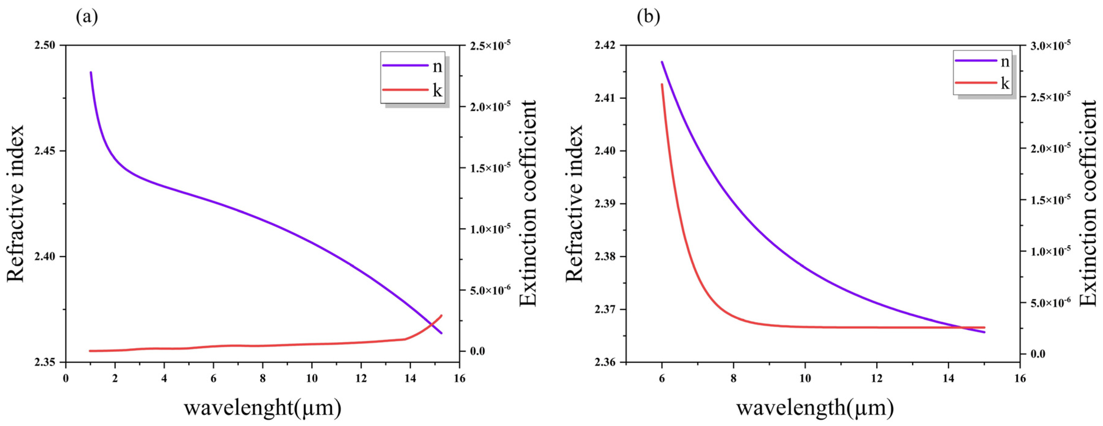
2.1. Substrates
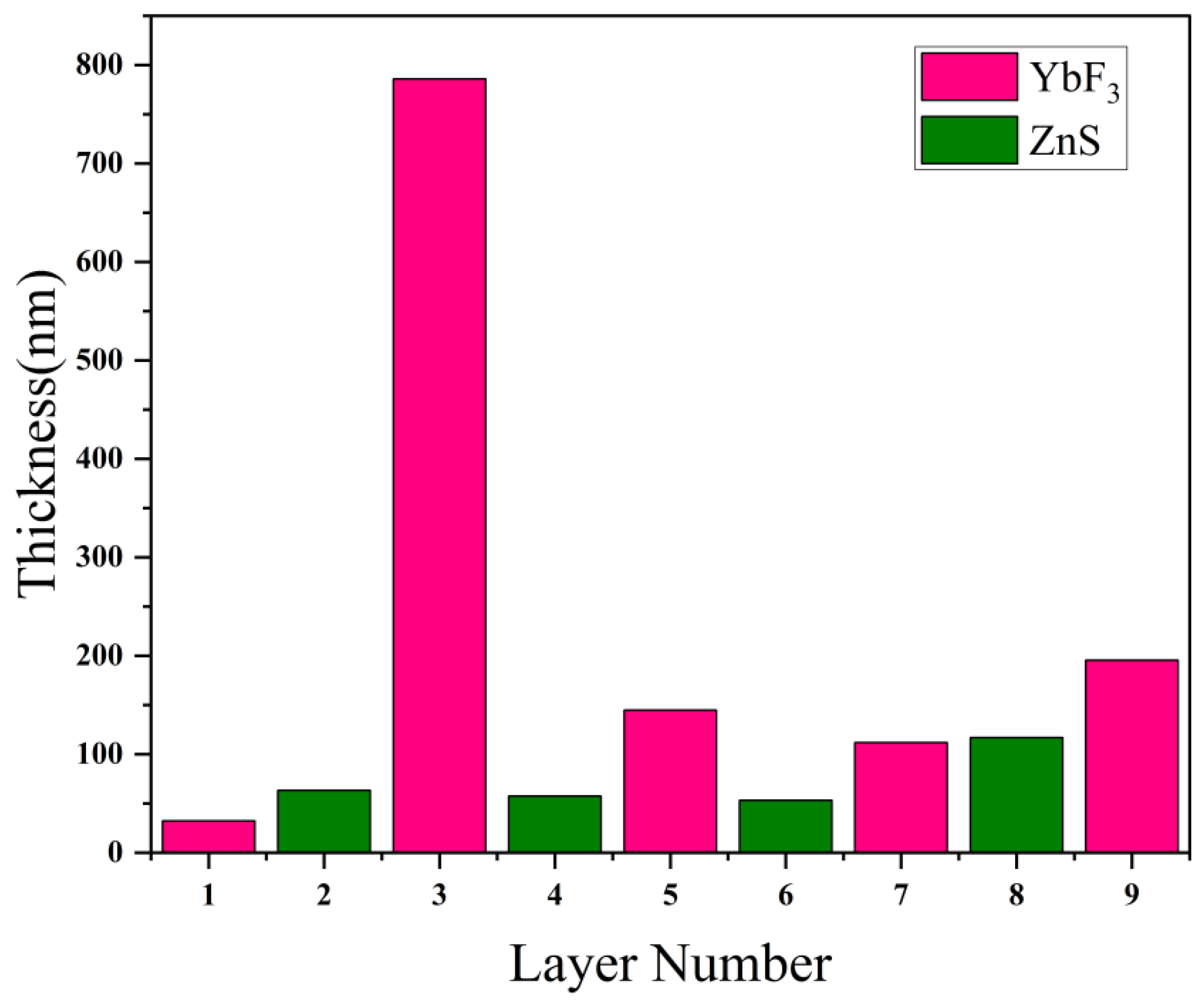
2.2. Design
2.3. Fabrication
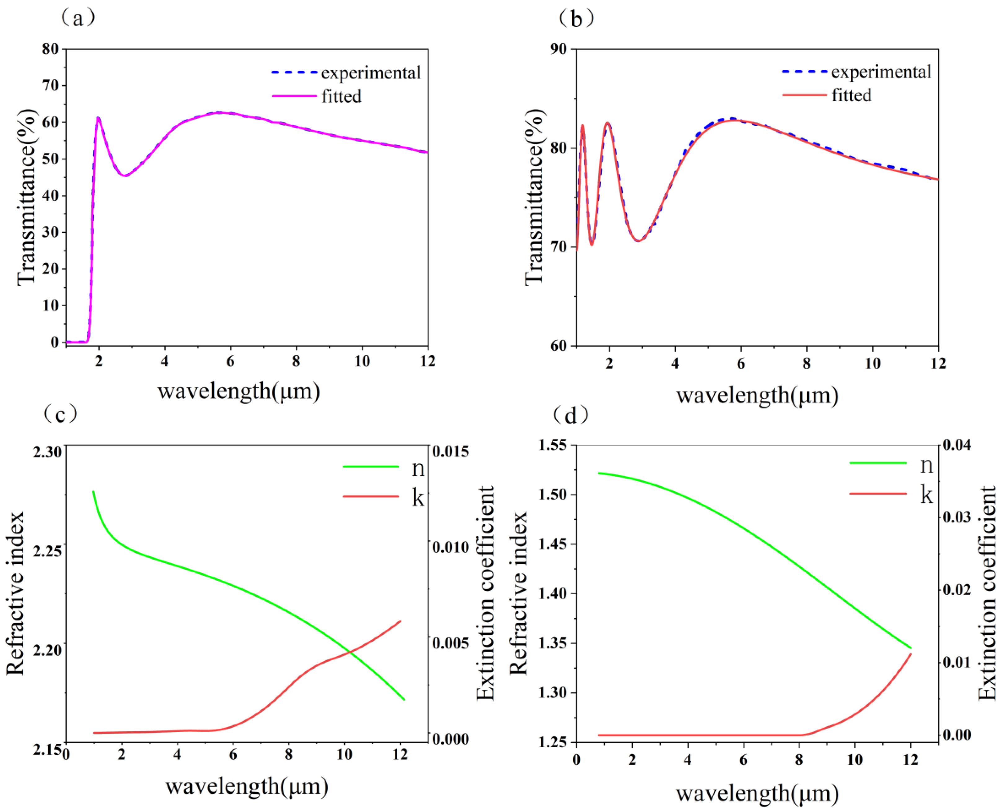
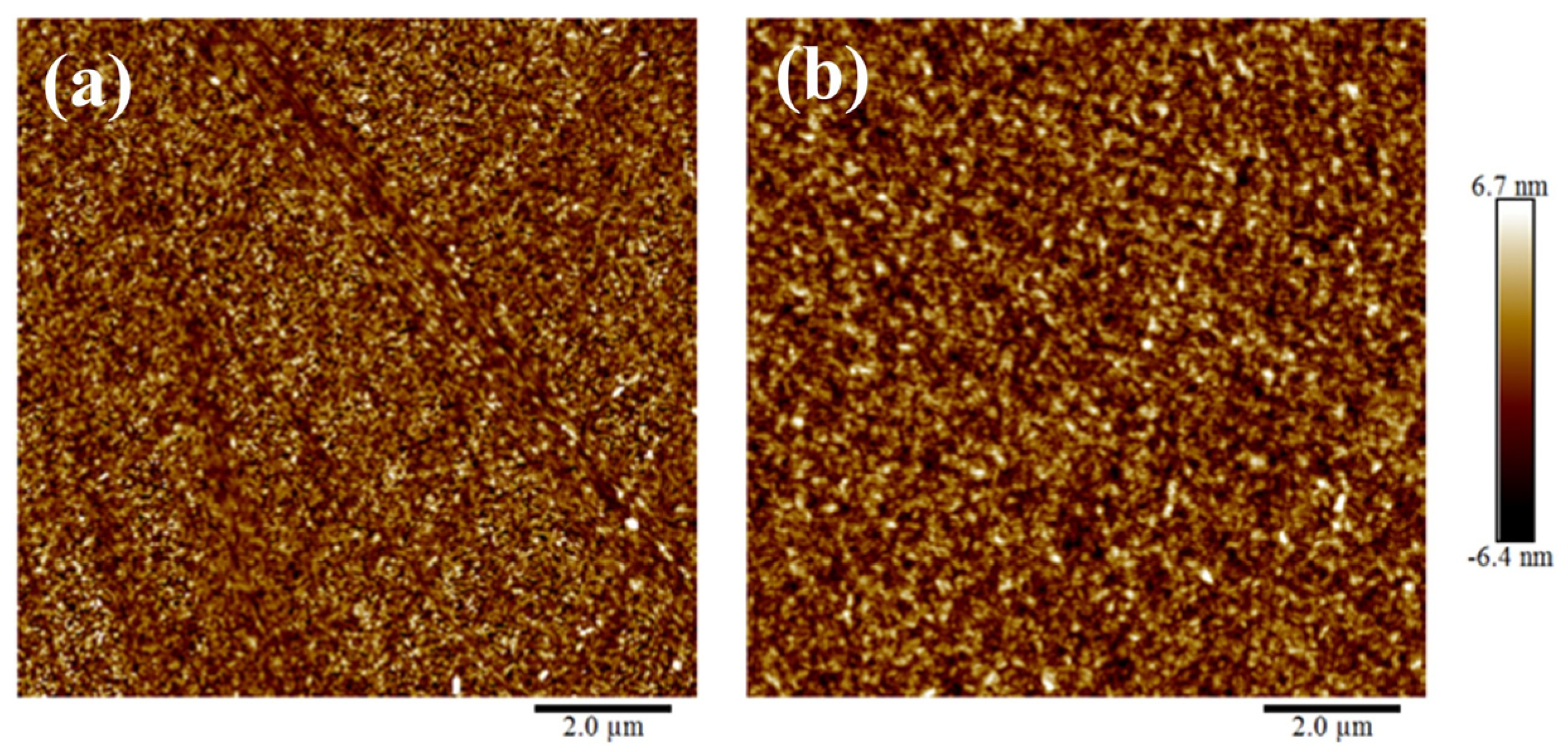
2.4. Characterization
3. Results and Discussion
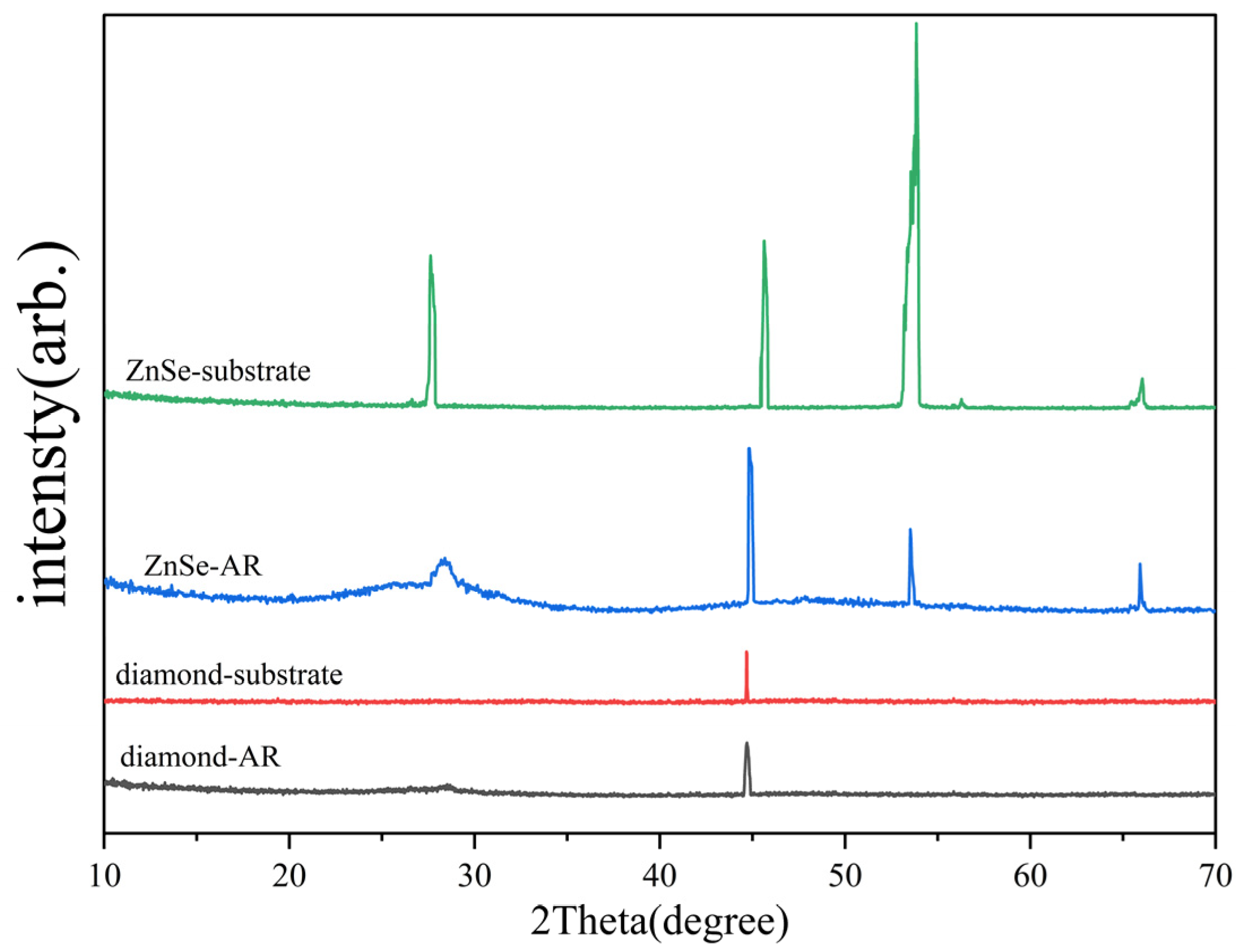
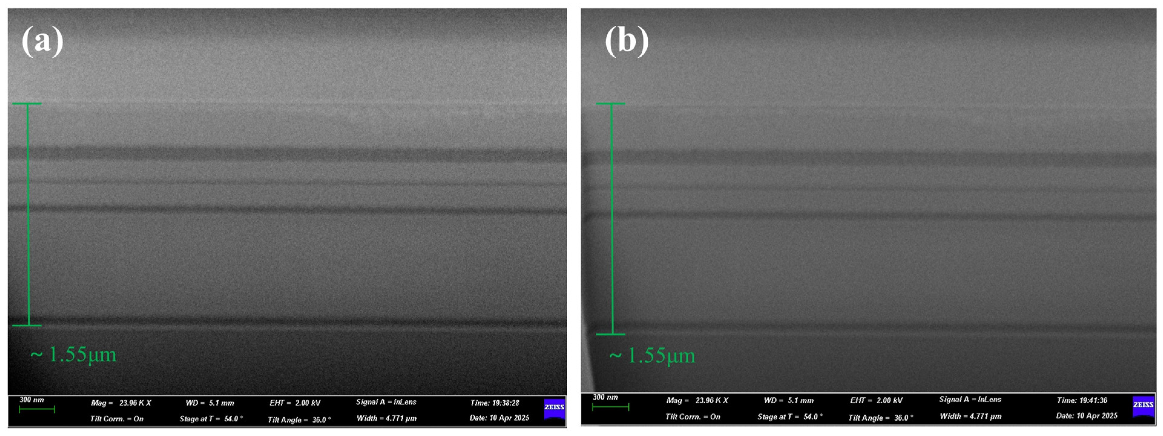
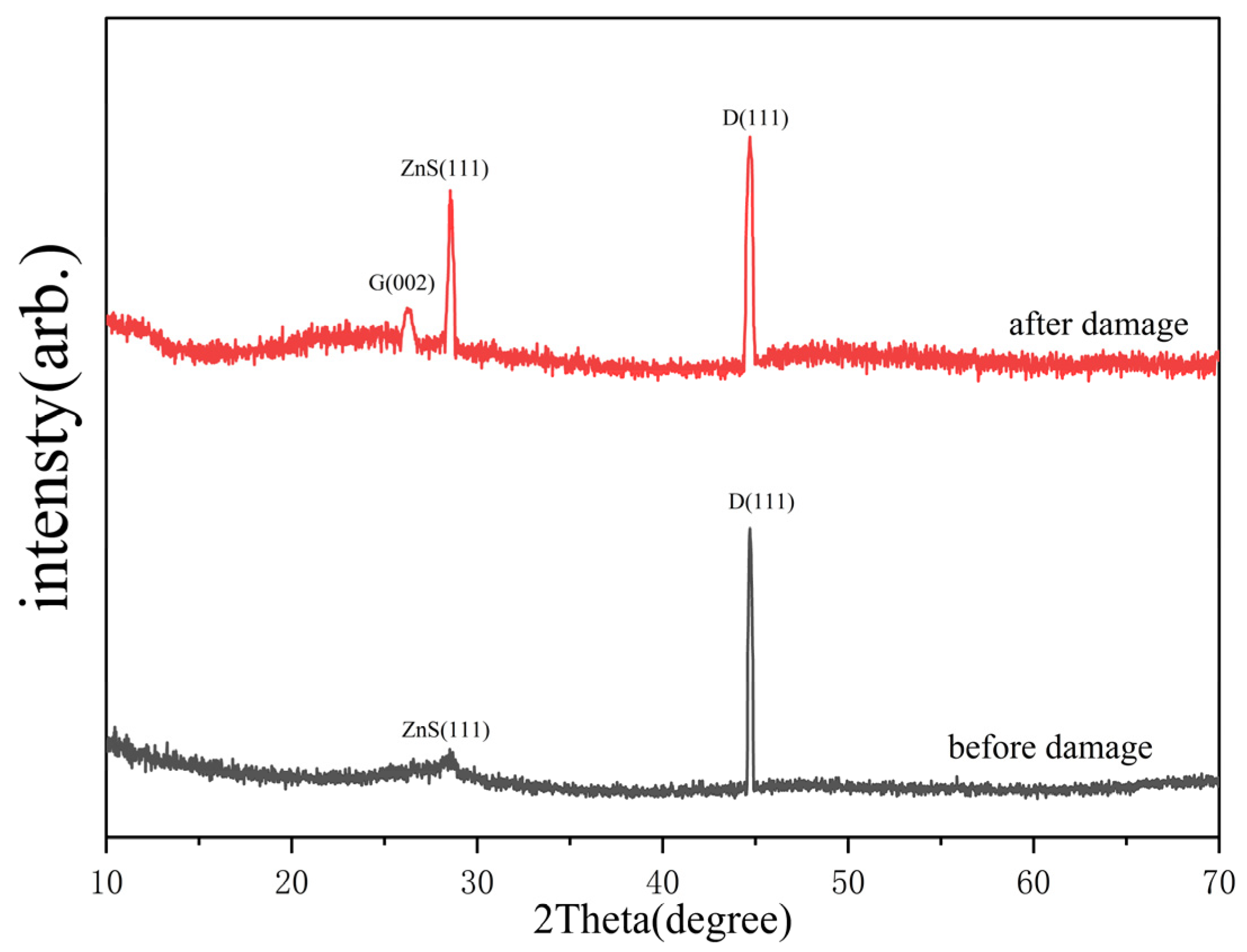
3.1. Coatings Performance
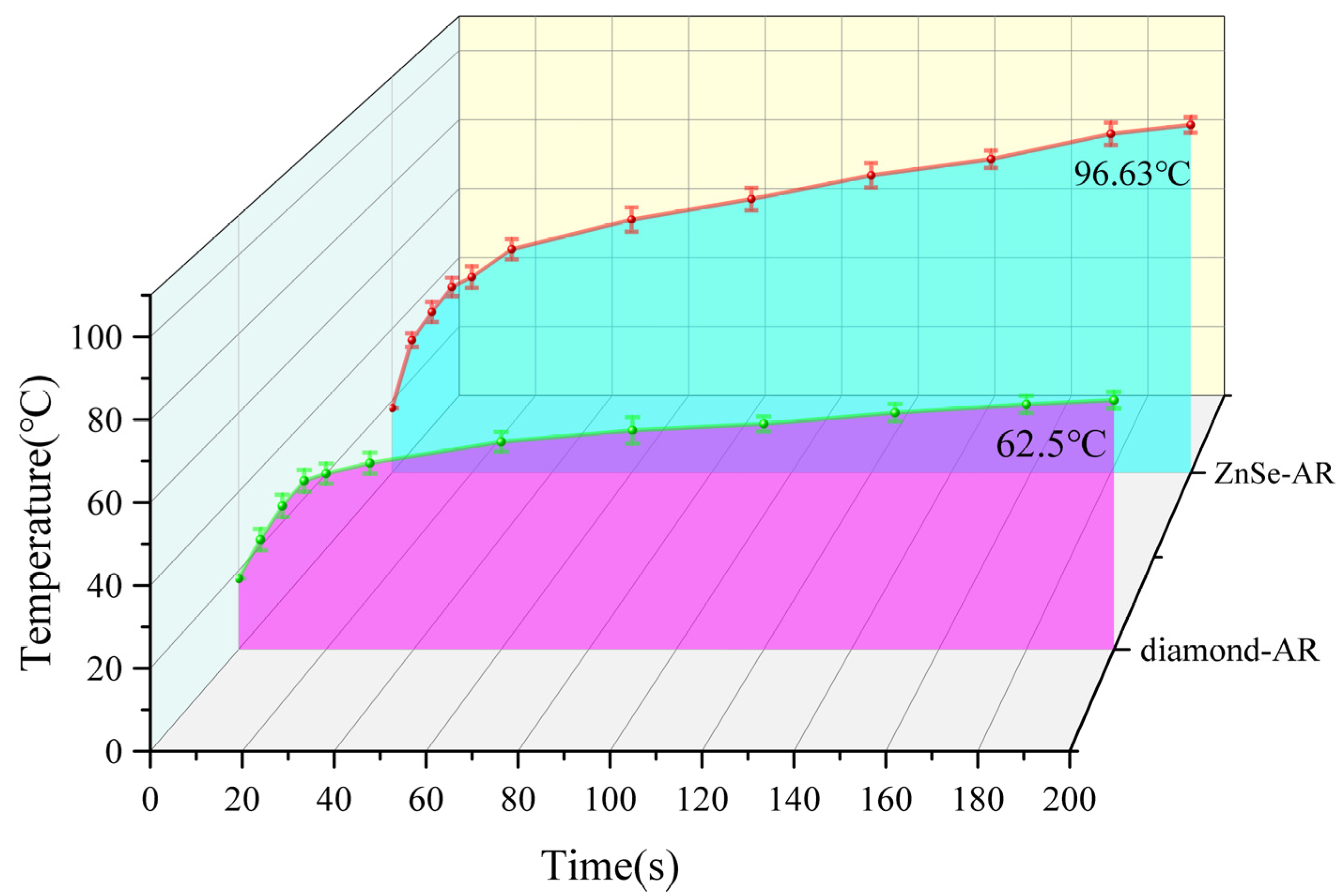
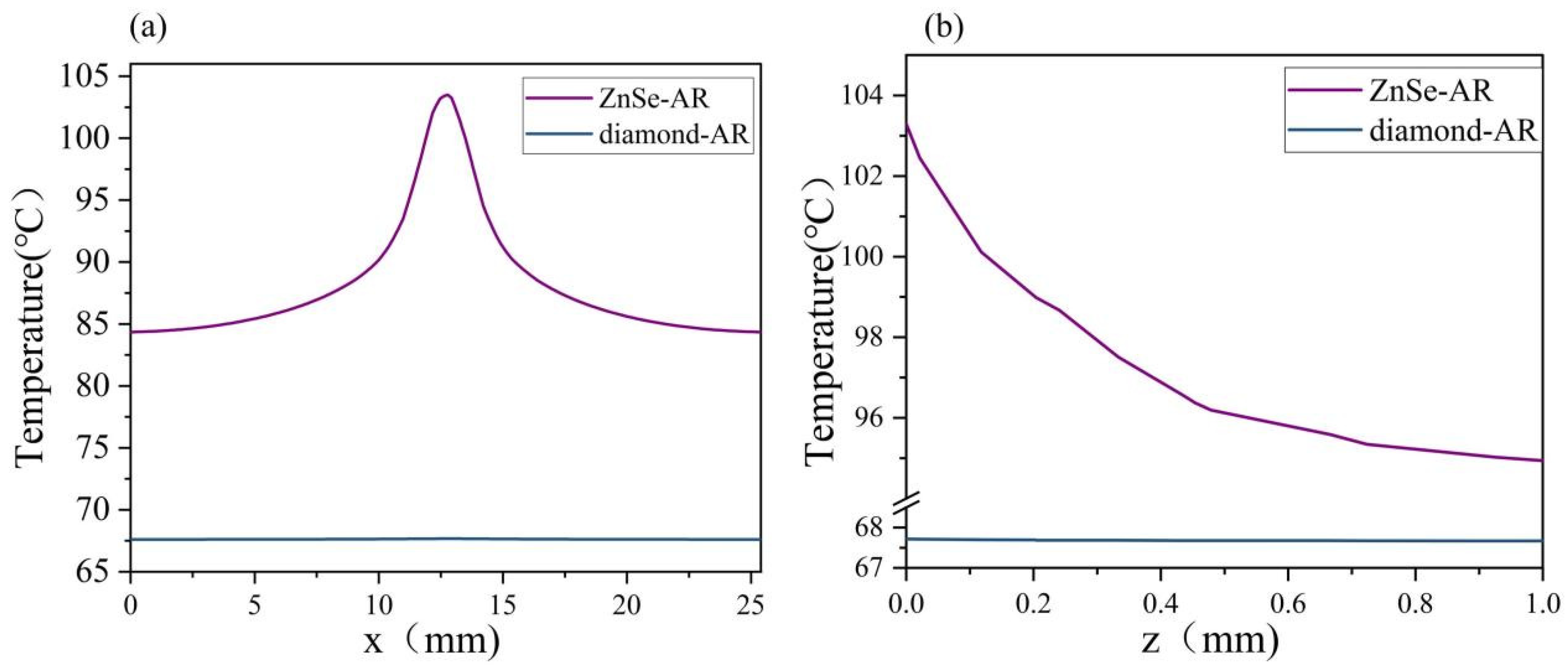
3.2. Temperature Rise
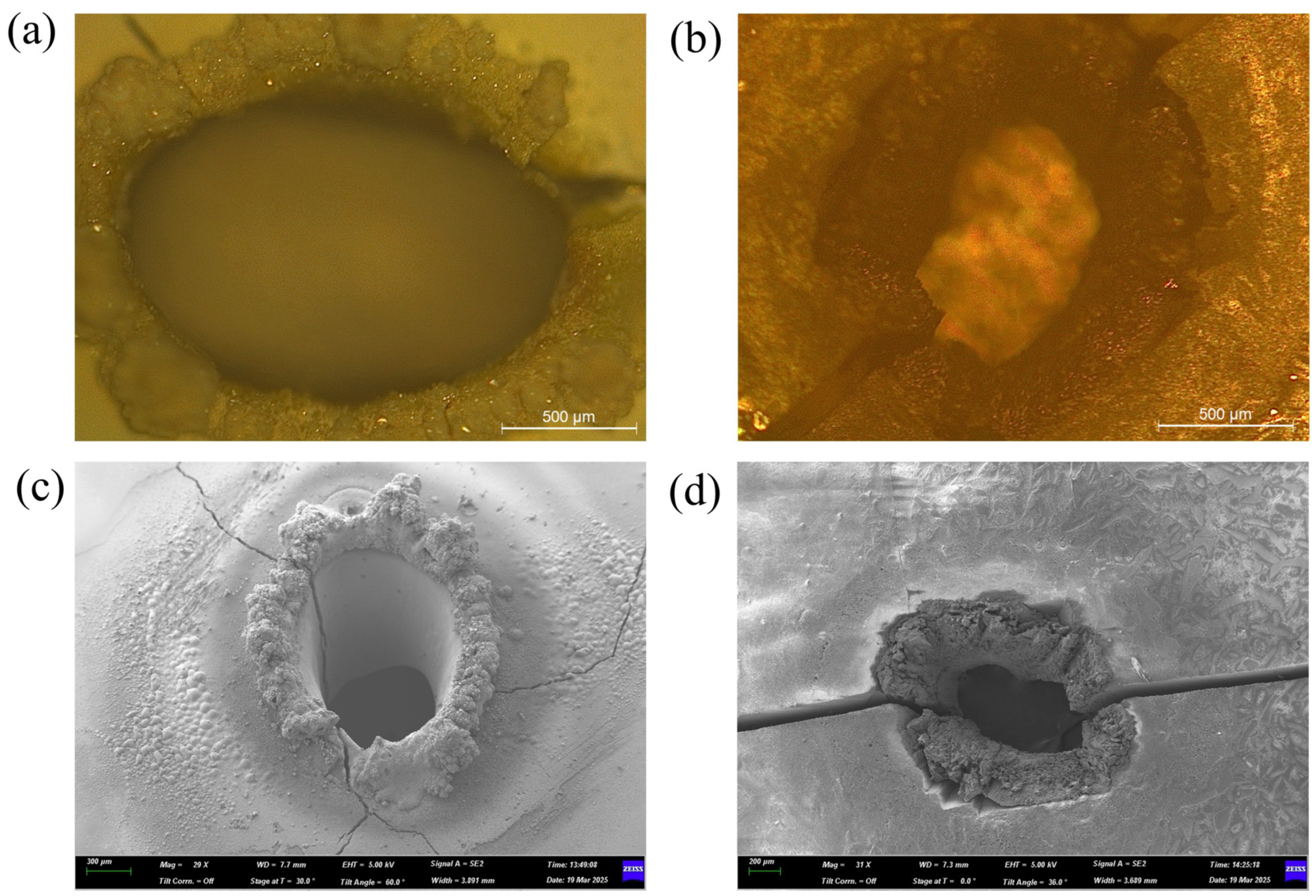
3.3. Laser-Induced Damage Threshold
4. Conclusions
- (1)
- Given the similar refractive indices of diamond and ZnSe, the same AR coating system was applied to both substrates. Furthermore, the transmission at 10.6 μm exceeded 98% on both substrates.
- (2)
- Due to the ultra-high thermal conductivity of diamond, the 10.6 μm AR coating deposited on the diamond substrate experiences a lower temperature rise under the same laser power density, with a 36% reduction in temperature rise compared to the coating deposited on the ZnSe substrate. Furthermore, it exhibits a more uniform temperature distribution, with lower temperature gradients both laterally and radially, which is expected to result in reduced thermally induced surface distortion.
- (3)
- Under 10.6 μm CW laser irradiation, the laser damage threshold of the AR coating on the ZnSe substrate is 11,890 W/cm2, while the threshold for the coating on the diamond substrate is 15,287 W/cm2, representing a 28.5% increase. The damage on the ZnSe substrate primarily manifests as interface melting, cracks, and substrate perforation. In contrast, the damage on the diamond substrate is characterized by melting, localized graphitization, fracture, and perforation.
Author Contributions
Funding
Institutional Review Board Statement
Informed Consent Statement
Data Availability Statement
Conflicts of Interest
References
- Gräf, S.; Staupendahl, G.; Krämer, A.; Müller, F.A. High Precision Materials Processing Using a Novel Q-Switched CO2 Laser. Opt. Lasers Eng. 2015, 66, 152–157. [Google Scholar] [CrossRef]
- England, R.J.; Noble, R.J.; Bane, K.; Dowell, D.H.; Ng, C.K.; Spencer, J.E.; Tantawi, S.; Wu, Z.; Byer, R.L.; Peralta, E.; et al. Dielectric Laser Accelerators. Rev. Mod. Phys. 2014, 86, 1337–1389. [Google Scholar] [CrossRef]
- Liu, W.; Yu, Z.; Sun, L.; Liu, Y.; Jia, Q.; Xu, H.; Sun, B. Microscale Laser-Driven Particle Accelerator Using the Inverse Cherenkov Effect. Phys. Rev. Appl. 2020, 14, 014018. [Google Scholar] [CrossRef]
- Sunahara, A.; Hassanein, A.; Tomita, K.; Namba, S.; Higashiguchi, T. Optimization of Extreme Ultra-Violet Light Emitted from the CO2 Laser-Irradiated Tin Plasmas Using 2D Radiation Hydrodynamic Simulations. Opt. Express 2023, 31, 31780. [Google Scholar] [CrossRef] [PubMed]
- Huang, H.; Zhou, X.; Zhang, J.; Li, J.; Lei, Q.; Rao, Y.; Zhou, M.; Wang, X.; Yuan, S.; Zhong, Y.; et al. Enhancing Surface Properties of Monocrystalline Silicon Wafers via Thermal Annealing for Solar Cell Texturing. Surf. Interfaces 2025, 62, 106219. [Google Scholar] [CrossRef]
- Keshavarz, M.; Tan, B.; Venkatakrishnan, K. Functionalized Stress Component onto Bio-Template as a Pathway of Cytocompatibility. Sci. Rep. 2016, 6, 35425. [Google Scholar] [CrossRef] [PubMed]
- Nakamura, T.; Koga, J.K.; Esirkepov, T.Z.; Kando, M.; Korn, G.; Bulanov, S.V. High-Power γ-Ray Flash Generation in Ultraintense Laser-Plasma Interactions. Phys. Rev. Lett. 2012, 108, 195001. [Google Scholar] [CrossRef]
- Apollonov, V.; Barchukov, A.; Prokhorov, A. Optical Distortion of Heated Mirrors in CO2-Laser Systems. IEEE J. Quantum Electron. 1974, 10, 505–508. [Google Scholar] [CrossRef]
- Brierley, C.J.; Beck, C.M.; Kennedy, G.R.; Metcalfe, J.; Wheatley, D. The Potential of CVD Diamond as a Replacement to ZnSe in CO2 Laser Optics. Diam. Relat. Mater. 1999, 8, 1759–1764. [Google Scholar] [CrossRef]
- Shi, C.; Sheng, Q.; Fu, S.; Sun, S.; Zhang, J.; Shi, W.; Yao, J. Power Scaling and Spectral Linewidth Suppression of Hybrid Brillouin/Thulium Fiber Laser. Opt. Express 2020, 28, 2948. [Google Scholar] [CrossRef]
- Zhou, L.; Tang, D. A Functionally Graded Structural Design of Mirrors for Reducing Their Thermal Deformations in High-Power Laser Systems by Finite Element Method. Opt. Laser Technol. 2007, 39, 980–986. [Google Scholar] [CrossRef]
- Yelisseyev, A.P.; Isaenko, L.I.; Lobanov, S.I.; Dostovalov, A.V.; Bushunov, A.A.; Tarabrin, M.K.; Teslenko, A.A.; Lazarev, V.A.; Shklyaev, A.A.; Babin, S.A.; et al. Effect of Antireflection Microstructures on the Optical Properties of GaSe. Opt. Mater. Express 2022, 12, 1593. [Google Scholar] [CrossRef]
- Yelisseyev, A.; Fedyaj, V.; Simonov, V.; Isaenko, L.; Lobanov, S.; Shklyaev, A.; Simanchuk, A.; Babin, S.; Dostovalov, A. Femtosecond Laser Direct Writing of Antireflection Microstructures on the Front and Back Sides of a GaSe Crystal. Photonics 2022, 9, 774. [Google Scholar] [CrossRef]
- Gurbatov, S.O.; Borodaenko, Y.M.; Mitsai, E.V.; Modin, E.; Zhizhchenko, A.Y.; Cherepakhin, A.B.; Shevlyagin, A.V.; Syubaev, S.A.; Porfirev, A.P.; Khonina, S.N.; et al. Laser-Induced Periodic Surface Structures on Layered GaSe Crystals: Structural Coloring and Infrared Antireflection. J. Phys. Chem. Lett. 2023, 14, 9357–9364. [Google Scholar] [CrossRef] [PubMed]
- Hardy, J.R.; Smith, S.D. Two-Phonon Infra-Red Lattice Absorption in Diamond. Philos. Mag. 1961, 6, 1163–1172. [Google Scholar] [CrossRef]
- Clark, C.D.; Davey, S.T. One-Phonon Infrared Absorption in Diamond. J. Phys. C Solid State Phys. 1984, 17, 1127–1140. [Google Scholar] [CrossRef]
- Cheng, L.; Zhu, S.; Ouyang, X.; Zheng, W. Bandgap Evolution of Diamond. Diam. Relat. Mater. 2023, 132, 109638. [Google Scholar] [CrossRef]
- Douglas-Hamilton, D.H.; Hoag, E.D.; Seitz, J.R.M. Diamond as a High-Power-Laser Window. J. Opt. Soc. Am. 1974, 64, 36. [Google Scholar] [CrossRef]
- Li, K.; Liu, Y.; Seaberg, M.; Chollet, M.; Weiss, T.M.; Sakdinawat, A. Wavefront Preserving and High Efficiency Diamond Grating Beam Splitter for X-Ray Free Electron Laser. Opt. Express 2020, 28, 10939. [Google Scholar] [CrossRef]
- Atikian, H.A.; Sinclair, N.; Latawiec, P.; Xiong, X.; Meesala, S.; Gauthier, S.; Wintz, D.; Randi, J.; Bernot, D.; DeFrances, S.; et al. Diamond Mirrors for High-Power Continuous-Wave Lasers. Nat. Commun. 2022, 13, 2610. [Google Scholar] [CrossRef]
- Karlsson, M.; Nikolajeff, F. Diamond Micro-Optics: Microlenses and Antireflection Structured Surfaces for the Infrared Spectral Region. Opt. Express 2003, 11, 502. [Google Scholar] [CrossRef] [PubMed]
- Kononenko, V.V.; Konov, V.I.; Pimenov, S.M.; Prokhorov, A.M.; Pavel’ev, V.S.; Soifer, V.A. Diamond Diffraction Optics for CO2 Lasers. Quantum Electron. 1999, 29, 9–10. [Google Scholar] [CrossRef]
- Komlenok, M.; Kononenko, T.; Sovyk, D.; Pavelyev, V.; Knyazev, B.; Ashkinazi, E.; Reshetnikov, A.; Komandin, G.; Pashinin, V.; Ralchenko, V.; et al. Diamond Diffractive Lens with a Continuous Profile for Powerful Terahertz Radiation. Opt. Lett. 2021, 46, 340. [Google Scholar] [CrossRef]
- Massart, M.; Union, P.; Scarsbrook, G.A.; Sussmann, R.S.; Muys, P.F. CVD-Grown Diamond: A New Material for High-Power CO2 Lasers; Bennett, H.E., Guenther, A.H., Kozlowski, M.R., Newnam, B.E., Soileau, M.J., Eds.; SPIE: Boulder, CO, USA, 1996; p. 177. [Google Scholar]
- Chiang, A.C.; Lin, Y.Y.; Huang, Y.C.; Babzien, M. Laser-Induced Damage Threshold at Chemical Vapor Deposition–Grown Diamond Surfaces for 200-Ps CO2 Laser Pulses. Opt. Lett. 2002, 27, 164. [Google Scholar] [CrossRef] [PubMed]
- Yu, J.; Xiang, X.; He, S.; Yuan, X.; Zheng, W.; Lü, H.; Zu, X. Laser-Induced Damage Initiation and Growth of Optical Materials. Adv. Condens. Matter Phys. 2014, 2014, 364627. [Google Scholar] [CrossRef]
- Amotchkina, T.; Trubetskov, M.; Hahner, D.; Pervak, V. Characterization of E-Beam Evaporated Ge, YbF3, ZnS, and LaF3 Thin Films for Laser-Oriented Coatings. Appl. Opt. 2020, 59, A40. [Google Scholar] [CrossRef]
- Dore, P.; Nucara, A.; Cannavò, D.; De Marzi, G.; Calvani, P.; Marcelli, A.; Sussmann, R.S.; Whitehead, A.J.; Dodge, C.N.; Krehan, A.J.; et al. Infrared Properties of Chemical-Vapor Deposition Polycrystalline Diamond Windows. Appl. Opt. 1998, 37, 5731. [Google Scholar] [CrossRef]
- Amotchkina, T.V.; Janicki, V.; Sancho-Parramon, J.; Tikhonravov, A.V.; Trubetskov, M.K.; Zorc, H. General Approach to Reliable Characterization of Thin Metal Films. Appl. Opt. 2011, 50, 1453. [Google Scholar] [CrossRef]
- Taguchi, T.; Kawakami, Y.; Yamada, Y. Interface Properties and the Effect of Strain of ZnSe/ZnS Strained-Layer Superlattices. Phys. B Condens. Matter 1993, 191, 23–44. [Google Scholar] [CrossRef]
- OptiLayer GmbH—OptiLayer GmbH. Available online: https://www.optilayer.org (accessed on 25 April 2025).
- Zhang, Y.; Xiong, S.; Huang, W. Study on Defects in ZnS/YbF3 Infrared Coatings on Silicon Substrates. Surf. Coat. Technol. 2017, 320, 3–6. [Google Scholar] [CrossRef]
- Peng, H. Experimental Studies of a Plane-Cone Resonator for High-Power, Transverse-Flow CO2 Laser. Opt. Eng. 2012, 51, 044204. [Google Scholar] [CrossRef]
- Dai, J.; Ji, X.; Niu, X.; Jiao, H.; Cheng, X.; Wang, Z.; Zhang, J. Advanced Deep Learning-Based Strategy for Optical Inversion Engineering of Optical Coatings. Opt. Express 2025, 33, 10057. [Google Scholar] [CrossRef]
- Komlenok, M.S.; Pivovarov, P.A.; Volodkin, B.O.; Pavelyev, V.S.; Anisimov, V.I.; Butuzov, V.V.; Sorochenko, V.R.; Nefedov, S.M.; Mineev, A.P.; Soifer, V.A.; et al. High-Damage-Threshold Antireflection Coatings on Diamond for CW and Pulsed CO2 Lasers. Laser Phys. Lett. 2018, 15, 036001. [Google Scholar] [CrossRef]
- Li, D.; Niu, X.; Xia, J.; Jiao, H.; Dun, X.; Zhang, J.; Cheng, X.; Wang, Z. Research on the Core Factors Affecting the Temperature Rise of Dichroic Mirrors in Wavelength Beam Combination System under High-Power CW Laser. Opt. Commun. 2024, 552, 130034. [Google Scholar] [CrossRef]
- Taylor, L.N.; Brown, A.K.; Pung, A.J.; Johnson, E.G.; Talghader, J.J. Continuous-Wave Laser Damage of Uniform and Nanolaminate Hafnia and Titania Optical Coatings. Opt. Lett. 2013, 38, 4292. [Google Scholar] [CrossRef]
- Jiao, H.; Ding, T.; Zhang, Q. Comparative Study of Laser Induce Damage of HfO2/SiO2 and TiO2/SiO2 Mirrors at 1064 nm. Opt. Express 2011, 19, 4059. [Google Scholar] [CrossRef] [PubMed]
- Li, X.; Zhang, X.; Ren, Y.; Wöhrl, N.; Lv, W.; Wang, H.; Li, Z. Study on the Transformation of Diamond into Graphene through High-Temperature Annealing. Ceram. Int. 2025, 51, 3029–3036. [Google Scholar] [CrossRef]
- Cadot, G.B.J.; Thomas, K.; Best, J.P.; Taylor, A.A.; Michler, J.; Axinte, D.A.; Billingham, J. Investigation of the Microstructure Change Due to Phase Transition in Nanosecond Pulsed Laser Processing of Diamond. Carbon 2018, 127, 349–365. [Google Scholar] [CrossRef]
- Yan, X.; Wei, J.; Guo, J.; Hua, C.; Liu, J.; Chen, L.; Hei, L.; Li, C. Mechanism of Graphitization and Optical Degradation of CVD Diamond Films by Rapid Heating Treatment. Diam. Relat. Mater. 2017, 73, 39–46. [Google Scholar] [CrossRef]


| Substrate | A0 | A1 | A2 | A3 | A4 |
|---|---|---|---|---|---|
| ZnSe | 5.957772 | 0.0136324 | 0.16445938 | 0.5302597 | 1292.685333 |
| Diamond | 5.512878 | 0.06116683 | 33.71128963 | 0.01220433 | 342.7813797 |
| Material | A0 | A1 | A2 | A3 | A4 |
|---|---|---|---|---|---|
| ZnS | 4.463858 | 0.1933777 | 2.5811114 | 0.1934265 | 2.580743 |
| YbF3 | 1.051848 | 0.2770681 | 0.3349626 | 0.5022135 | 6.775195 |
| Substrate Material | Thermal Expansion (10−6K−1) | Specific Heat (J/(kg−1·K−1)) | Density (kg/m3) | Thermal Conductivity Coefficient (W/(m·K)) | Young’s Modulus (GPa) | Poisson’s Ratio | 10.6 µm Extinction Coefficient |
|---|---|---|---|---|---|---|---|
| ZnSe | 7.1 | 339 | 6100 | 16 | 67.2 | 0.28 | 6.01 × 10⁻⁷ |
| Diamond | 1.1 | 515 | 3520 | 2000 | 1000 | 0.1 | 2.61 × 10⁻⁶ |
| Sample | Spot Size | Power (W) | LIDT (W/cm−2) |
|---|---|---|---|
| ZnSe-AR | 1.5 mm | 210 | 11,890 |
| Diamond-AR | 1.5 mm | 270 | 15,287 |
Disclaimer/Publisher’s Note: The statements, opinions and data contained in all publications are solely those of the individual author(s) and contributor(s) and not of MDPI and/or the editor(s). MDPI and/or the editor(s) disclaim responsibility for any injury to people or property resulting from any ideas, methods, instructions or products referred to in the content. |
© 2025 by the authors. Licensee MDPI, Basel, Switzerland. This article is an open access article distributed under the terms and conditions of the Creative Commons Attribution (CC BY) license (https://creativecommons.org/licenses/by/4.0/).
Share and Cite
Zi, X.; Niu, X.; Jiao, H.; Jiao, S.; Ji, X.; Li, D.; Jiang, B.; Zhang, J.; Cheng, X.; Wang, Z.; et al. Research on Thermal Effect and Laser-Induced Damage Threshold of 10.6 µm Antireflection Coatings Deposited on Diamond and ZnSe Substrates. Coatings 2025, 15, 536. https://doi.org/10.3390/coatings15050536
Zi X, Niu X, Jiao H, Jiao S, Ji X, Li D, Jiang B, Zhang J, Cheng X, Wang Z, et al. Research on Thermal Effect and Laser-Induced Damage Threshold of 10.6 µm Antireflection Coatings Deposited on Diamond and ZnSe Substrates. Coatings. 2025; 15(5):536. https://doi.org/10.3390/coatings15050536
Chicago/Turabian StyleZi, Xiong, Xinshang Niu, Hongfei Jiao, Shuai Jiao, Xiaochuan Ji, Dongdong Li, Binbin Jiang, Jinlong Zhang, Xinbin Cheng, Zhanshan Wang, and et al. 2025. "Research on Thermal Effect and Laser-Induced Damage Threshold of 10.6 µm Antireflection Coatings Deposited on Diamond and ZnSe Substrates" Coatings 15, no. 5: 536. https://doi.org/10.3390/coatings15050536
APA StyleZi, X., Niu, X., Jiao, H., Jiao, S., Ji, X., Li, D., Jiang, B., Zhang, J., Cheng, X., Wang, Z., & Xin, Z. (2025). Research on Thermal Effect and Laser-Induced Damage Threshold of 10.6 µm Antireflection Coatings Deposited on Diamond and ZnSe Substrates. Coatings, 15(5), 536. https://doi.org/10.3390/coatings15050536