Article

Oxidation Resistance and Mechanical Properties of Mo2N/MoSi2 Multi-Layer Films Prepared by Reactive Magnetron Sputtering

1
School of Mechanical Engineering and Automation, Wuhan Textile University, Wuhan 430073, China
2
Hubei Key Laboratory of Digital Textile Equipment, Wuhan Textile University, Wuhan 430073, China
3
Key Laboratory of Materials Physics, Institute of Solid State Physics, Chinese Academy of Sciences, Hefei 230031, China
4
Analytical and Testing Center, Wuhan Textile University, Wuhan 430073, China
*
Authors to whom correspondence should be addressed.
Coatings 2025, 15(4), 457; https://doi.org/10.3390/coatings15040457
Submission received: 23 February 2025 / Revised: 2 April 2025 / Accepted: 10 April 2025 / Published: 12 April 2025

Abstract

:
To investigate the properties of Mo2N/MoSi2 multi-layer films, pure Mo2N films, pure MoSi2 films, and Mo2N/MoSi2 multi-layer films with 4, 8, 12, 16, and 20 layers were prepared using magnetron sputtering. Before and after oxidation, the phase structure, morphology, and elemental composition of the films were analyzed using X-ray diffraction, field-emission scanning electron microscopy, atomic force microscopy, and energy-dispersive spectroscopy. The mechanical properties of the films were characterized by nanoindentation. The results indicate that the Mo2N/MoSi2 multi-layer films consist of cubic Mo2N and hexagonal MoSi2. As the number of layers increases, the thickness of the Mo2N and MoSi2 individual layers gradually decreases, significant changes occur in the surface and cross-sectional morphology of the Mo2N/MoSi2 multi-layer films, and the average grain size decreases with an increase in the number of layers. The Mo2N/MoSi2 multi-layer films exhibit superior oxidation resistance compared to the pure Mo2N films. However, as the thickness of an individual layer increases, the oxidation resistance of the multi-layer films decreases. The hardness of Mo2N/MoSi2 multi-layer films increases from 21.65 ± 1.08 GPa for the 4-layer film to 32.14 ± 1.38 GPa for the 20-layer film.

1. Introduction

In the past several decades, transition metal nitride (TMN) coatings, such as TiN, MoN, CrN, and WN, have been extensively applied in cutting tools because of their ability to reduce the cost and extend the tool life. TMN films are highly valued for their combination of high hardness, low friction coefficient, excellent electrical conductivity, and strong resistance to corrosion and oxidation [1,2,3,4,5,6]. Among these films, Mo2N films have gained significant attention because of their excellent wear characteristics and strong adherence to iron-based materials [7,8,9,10]. However, Mo2N films are susceptible to oxidation at high temperatures and possess lower hardness than TiN [11]. Therefore, enhancing the oxidation resistance and hardness of Mo2N is a critical challenge. Composite structures are known to considerably enhance the characteristics of TMN films [12,13]. To enhance the protective performance of Mo2N films, researchers have incorporated various elements into Mo2N to develop composite structures [14,15,16,17]. Prior research indicates that doping Si elements into Mo-N to form MoSiN films results in a finer crystal structure, enhancing the hardness and wear resistance of the films while simultaneously reducing the friction coefficient. However, this coating has some drawbacks, such as poor adhesion, limited improvement in mechanical properties, and insufficient enhancement of oxidation resistance. Further, it has not yet achieved the expected significant improvement and still requires further optimization and refinement [18,19].
The multi-layer structure is another way to improve the performance of TMN films, which can effectively utilize the advantages of each material by alternately depositing layers of different substances. The interfaces with a superlattice structure notably improve the hardness of the nitride film [20,21,22,23]. These interfaces also act as barriers to oxygen diffusion at high temperatures, enhancing oxidation resistance [24,25,26,27,28]. It is widely known Molybdenum silicide (MoSi2) is an important high-temperature structural material that has been widely utilized in coating technology because of its low density (6.24 g/cm3), high melting point (2030 °C), good thermal conductivity, and high working temperature (≤1850 °C) [29,30]. Under high-temperature conditions, the silica protective layer formed on the surface of the MoSi2 films can prevent further oxidation [31]. Therefore, Mo2N/MoSi2 multi-layer films with MoSi2 surface layers may exhibit high hardness and good oxidation resistance.
In this study, Mo2N/MoSi2 multi-layer films with various numbers of layers were fabricated using magnetron sputtering. The microstructure, oxidation resistance, and mechanical performance of Mo2N/MoSi2 multi-layer films were systematically analyzed.

2. Materials and Methods

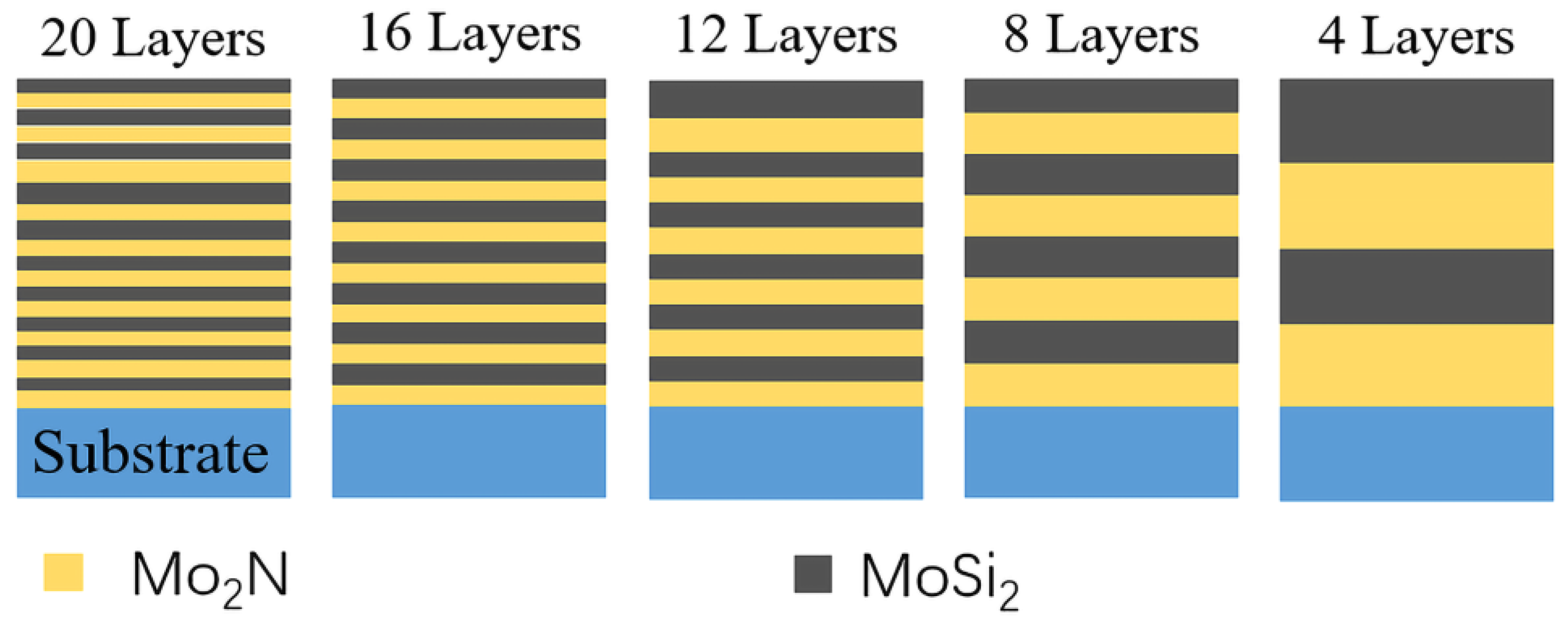
2.1. Preparation of Films

Mo2N, MoSi2, and Mo2N/MoSi2 multi-layer films were deposited on Si (100) and stainless steel substrates using Mo target and Si targets in a TRP-450 three-target automatic magnetron sputtering system manufactured by Shenyang Scientific Instrument Co., Ltd., Chinese Academy of Sciences (Shenyang, China). The purity of both the Mo and Si targets was 99.95%, and the diameter of each target was 60 mm. The Mo targets were mounted on DC sputtering sources, and the Si targets were mounted on RF sputtering sources. Before installation, the Si and stainless steel substrates were first ultrasonically cleaned with ethanol for 16 min, followed by ultrasonic cleaning with deionized water for 5 min. After cleaning and drying, the substrates were secured to a substrate holder. In this sputtering system, the substrate holder was positioned above the target to ensure that its surface remained horizontal. The target surface was inclined at an angle of 15° relative to the horizontal plane, and the distance between the target center and the substrate holder center was maintained at 100 mm. After fixing the targets and substrates, the vacuum chamber pressure was reduced to 1 × 10⁻³ Pa. The substrates were then heated to 450 °C and maintained at this temperature for 5 min. Subsequently, the sputtering gas was fed into the gas mixing chamber, where it was allowed to mix for 3 min before being transferred into the vacuum chamber. The sputtering pressure was adjusted to a predetermined value, and sputtering was initiated.
For the preparation of Mo2N films, ultra-high-purity Ar and N2 gases (99.999%) were thoroughly mixed and introduced into a vacuum chamber. The flow rates of nitrogen (N2) and argon (Ar) were 10 and 20 sccm, respectively. After adjusting the sputtering pressure to 0.78 Pa, the Mo target power supply was turned on, and the sputtering power was set to 80 W. For the preparation of MoSi2 films, ultra-high-purity Ar (99.999%) was introduced into the gas mixing chamber for 3 min and then injected into the vacuum chamber at a flow rate of 25 sccm. The vacuum chamber pressure was maintained at 0.78 Pa, and the sputtering power was set at 80 W for the Mo target and 100 W for the Si target, respectively. Mo2N/MoSi2 multi-layer films with the bottom layer of Mo2N and the surface layer of MoSi2 were prepared by alternately stacking Mo2N and MoSi2. The 4-, 8-, 12-, 16-, and 20-layer multi-layer films were fabricated following the aforementioned method. The detailed parameters are listed in Table 1.
For all samples, the rotational speed of the substrate holder was set to 5 rpm, and the total deposition time was 7200 s. A schematic of the Mo2N/MoSi2 multi-layer films is shown in Figure 1.
To investigate the oxidation resistance of Mo2N films, MoSi2 films, and Mo2N/MoSi2 multi-layer films, samples with varying layer numbers were heated in a tube atmosphere furnace (TFN-12t, Ningbo Taifno PTFE Plastic Products Co., Ltd., Ningbo, China) to 450, 500, 550, and 600 °C in air, with the ambient relative humidity maintained at 78 ± 2%. The heating rate was set to 4 °C/min. The films were maintained at the target temperature for 10 min and then cooled naturally to ambient conditions (25 °C). The oxidation temperature range and holding time were chosen to prevent the excessive volatilization of MoO3.

2.2. Characterization of Films

The crystallographic phases of the films, both before and after oxidation, were investigated using an X-ray diffractometer (XRD, PANalytical Empyrean, Panaco, Almelo, The Netherlands) monochromatized Cu Kα radiation with a wavelength of 1.5406 Å operated at 40 kV and 40 mA. The 2θ scanning range was set from 10° to 60° with a step size of 0.013° and scanning speed of 4°·min−1.
The surface and cross-sectional morphologies of the films were observed using a field-emission scanning electron microscope (FESEM; SU-5000, Hitachi, Tokyo, Japan) fitted with an energy-dispersive X-ray spectroscopy (EDS) analyzer. All samples were gold-coated prior to testing. EDS analysis was performed to confirm the distribution of elements in the samples. The three-dimensional surface topographies of the films were analyzed using an atomic force microscope (AFM, Dimension 3100, Bruker, Billerica, MA, USA) in tapping mode with a scan area of 5 × 5 μm2.
The mechanical properties (hardness and elastic modulus) were measured using a nanoindentation system (G200; Keysight Technologies, Santa Rosa, CA, USA). Continuous stiffness data were obtained using a vibration tip with a frequency of 42 Hz and an amplitude of 2 nm. The indentation depth was set to 900 nm for all samples. Eight evenly spaced test points were selected on each film surface for repeated measurements to ensure the statistical reliability of the data. Based on the Oliver-Pharr method, the hardness and elastic modulus of the films were calculated by analyzing the experimentally obtained data [32].

3. Results and Discussion

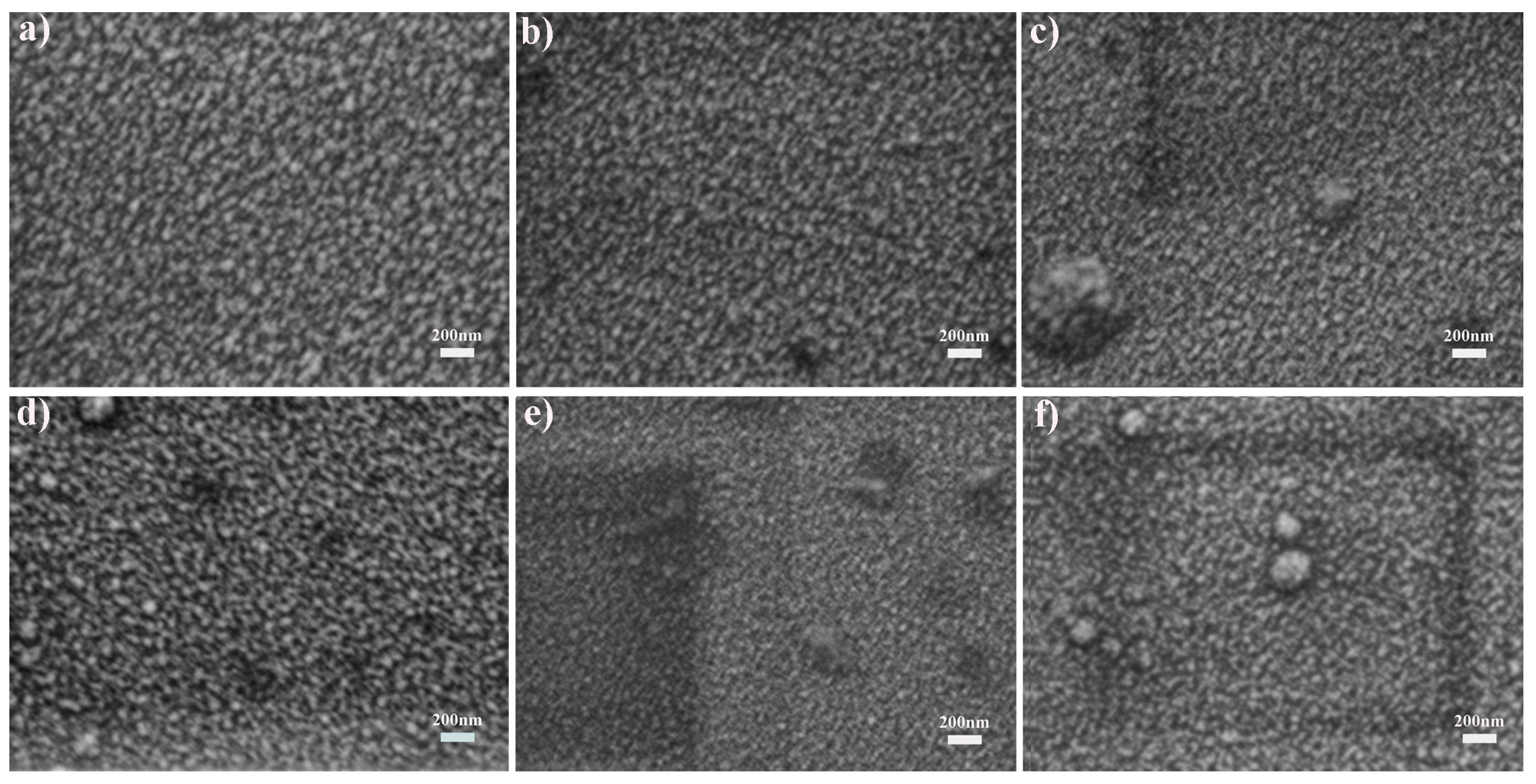
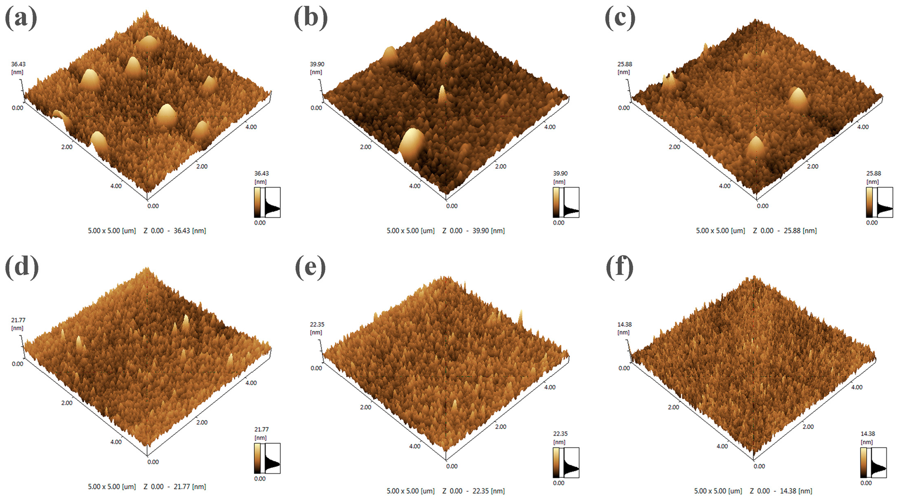
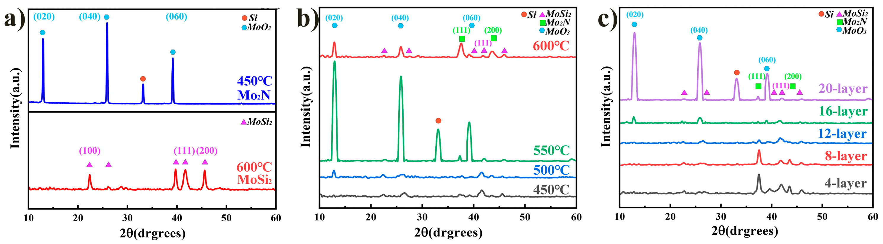
3.1. Structure of As-Received Films

Figure 2 exhibits the surface morphologies of the MoSi2 film and Mo2N/MoSi2 multi-layer films, as characterized by FESEM. Figure 2a shows that the particles in the MoSi2 film exhibit a roughly rounded shape with a tightly packed arrangement. As shown in Figure 2b, the surface morphology of the 4-layer film resembles that of pure MoSi2. However, as shown in Figure 2c, the surface of the 8-layer film contains large particles. In Figure 2d–f, the number of large particles on the surface increases with an increase in the number of layers. The results demonstrate that the number of layers profoundly affects the structure of Mo2N/MoSi2 multi-layer films.
The cross-sectional morphologies and thicknesses of the MoSi2 film and Mo2N/MoSi2 multi-layer films are shown in Figure 3. The total thicknesses of the 4-, 8-, 12-, 16-, and 20-layer films is about 0.65, 0.67, 0.63, 0.57, and 0.70 μm, respectively. The thicknesses of the Mo2N individual layers corresponding to the 4-, 8-, 12-, 16-, and 20-layer films is about 105, 41, 33, 27, and 25 nm, respectively, and the thicknesses of the MoSi2 individual layers corresponding to the 4-, 8-, 12-, 16-, and 20-layer films is about 220, 126, 71, 45, and 43 nm, respectively. The results illustrate that as the layer number increases, the thickness of the individual layer gradually decreases. In Figure 3a, the columnar structure at the bottom of the MoSi2 film is not distinct, while the middle and upper layers exhibit a well-defined columnar structure. For the multi-layer films, the Mo2N layer (bright) and MoSi2 layer (dark) are easily distinguished and tightly bonded, suggesting that the structure of the multi-layer films aligns with the design expectations. With an increase in the number of layers, the cross-sectional structure of the Mo2N/MoSi2 multi-layer films gradually becomes more uniform, the columnar structure is refined, and the interfaces between the layers become clearer. As shown in Figure 3b–e, the surface layers of the multi-layer films exhibit a dense, uniform, and continuous structure with good integrity, and no obvious defects are observed. However, as shown in Figure 3f, obvious pinholes are observed in the 20-layer film. The formation of this defect can be explained in two ways: One reason for this is the internal stress within the film. As the layer number increases, the increasing number of interfaces leads to a gradual accumulation of internal stress. When the stress exceeds the ultimate strength of the material, fractures or cracks occur in the film [33]. Another reason may be attributed to the gradual decrease in the thickness of the surface MoSi2 layer, which cannot cover the underlying Mo2N layer with an increasing number of layers.
Figure 4a,b shows the XRD patterns of the Mo2N film, MoSi2 film, and Mo2N/MoSi2 multi-layer films. In Figure 4a, the pure Mo2N film exhibits diffraction peaks at 37.4° and 43.5°, corresponding to the (111) and (200) crystal planes of cubic Mo2N (PDF # 00-025-1366), respectively. The pure MoSi2 film exhibits diffraction peaks at 22.2°, 26.0°, 39.0°, 41.3°, and 45.3°, corresponding to the (100), (101), (110), (111), and (200) crystal planes of hexagonal MoSi2 (PDF # 01-081-0167). In Figure 4b, for all Mo2N/MoSi2 multi-layer films, diffraction peaks corresponding to the (100), (101), (110), (111), and (200) planes of MoSi2 and the (111) and (200) planes of Mo2N were observed, indicating that the Mo2N/MoSi2 multi-layer films consist of Mo2N and MoSi2.
As shown in Figure 4a,b, it can be observed that as the thickness of the individual layer film decreases, the full width at half maximum of the diffraction peaks widens. Although there are many factors that affect the full width at half maximum of XRD diffraction, including instrumental factors, the presence of defects in a perfect lattice, differences in strain between different grains, and the grain size. For nanomaterials with a grain size of less than 100 nm, the influence of grain size on the diffraction peak width dominates [34]. In this article, all samples were tested using the same instrument; hence, the influence of the instrument can be ignored. The change in half peak width is mainly caused by the change in grain size in this article. Based on the XRD patterns, the average grain sizes of Mo2N and MoSi2 in the Mo2N/MoSi2 films were calculated using the Scherrer formula [35]:
D = K λ B c o s θ
where D is the grain size (nm) and K is the Scherrer constant. Generally, the constant K ranges from 0.8 to 1.39. For film samples, some authors usually assume K = 1 or 0.9 [36,37,38], here, K = 0.9, λ is the wavelength of Cu Kα (1.5406 Å), θ is the Bragg angle of XRD (°), and B is the full width at half maximum (FWHM).
Figure 4c,d shows the average grain sizes of Mo2N and MoSi2 in the Mo2N/MoSi2 multi-layer films calculated according to Equation (1). In Figure 4c, the average Mo2N grain sizes corresponding to the 4-, 8-, 12-, 16-, and 20-layer films are 26.8 ± 1.15, 21.8 ± 2.35, 19.2 ± 2.25, 15.5 ± 1.85, and 12.6 ± 0.25, respectively. In Figure 4d, the average MoSi2 grain size corresponding to 4-, 8-, 12-, 16-, and 20-layer films is 25.0 ± 2.23, 20.9 ± 2.14, 18.4 ± 0.99, 16.9 ± 1.25, and 15.5 ± 0.45 nm, respectively. These results indicate that as the thickness of an individual layer decreases, the average grain size in the Mo2N/MoSi2 multi-layer films decreases gradually. The reduction in grain size is ascribed to the confinement effects exerted by the interlayer boundaries, which inhibit grain growth, ultimately leading to smaller grains. This phenomenon has been observed in additional multi-layer film systems [39].
Figure 5 shows the results of EDS for the MoSi2 film. The Mo content of the pure MoSi2 film is 29.8 at.% (atomic percentage), while the Si content is 57.8 at.%. Pt in the test results was attributed to the vapor deposition Pt treatment of the sample surface before SEM testing, while the other elements were attributed to pollution in the air. The data indicate that there is approximately a 1:2 atomic ratio between Mo and Si, which is consistent with the ideal ratio for MoSi2 compounds. This result is consistent with the XRD data, indicating that MoSi2 films can be successfully prepared by simultaneously sputtering Mo and Si targets in an Ar environment.
The 3D surface topographies of the MoSi2 film and MoSi2/Mo2N multi-layer films analyzed by AFM are shown in Figure 6. The surface topography of the MoSi2 film exhibits significant undulations and fluctuations, with a maximum height (Hm) of 36.448 nm and an average roughness (Ra) of 4.351 nm. For MoSi2/Mo2N multi-layer films, with an increasing number of layers, the Hm decreases from 39.9 nm for the 4-layer film to 14.38 nm for the 20-layer film, while the Ra decreases from 2.492 nm for the 4-layer film to 0.955 nm for the 20-layer film. The above phenomena show that the grains on the film surface are refined, and the uniformity of the grains changes well with an increasing number of layers in the local area.

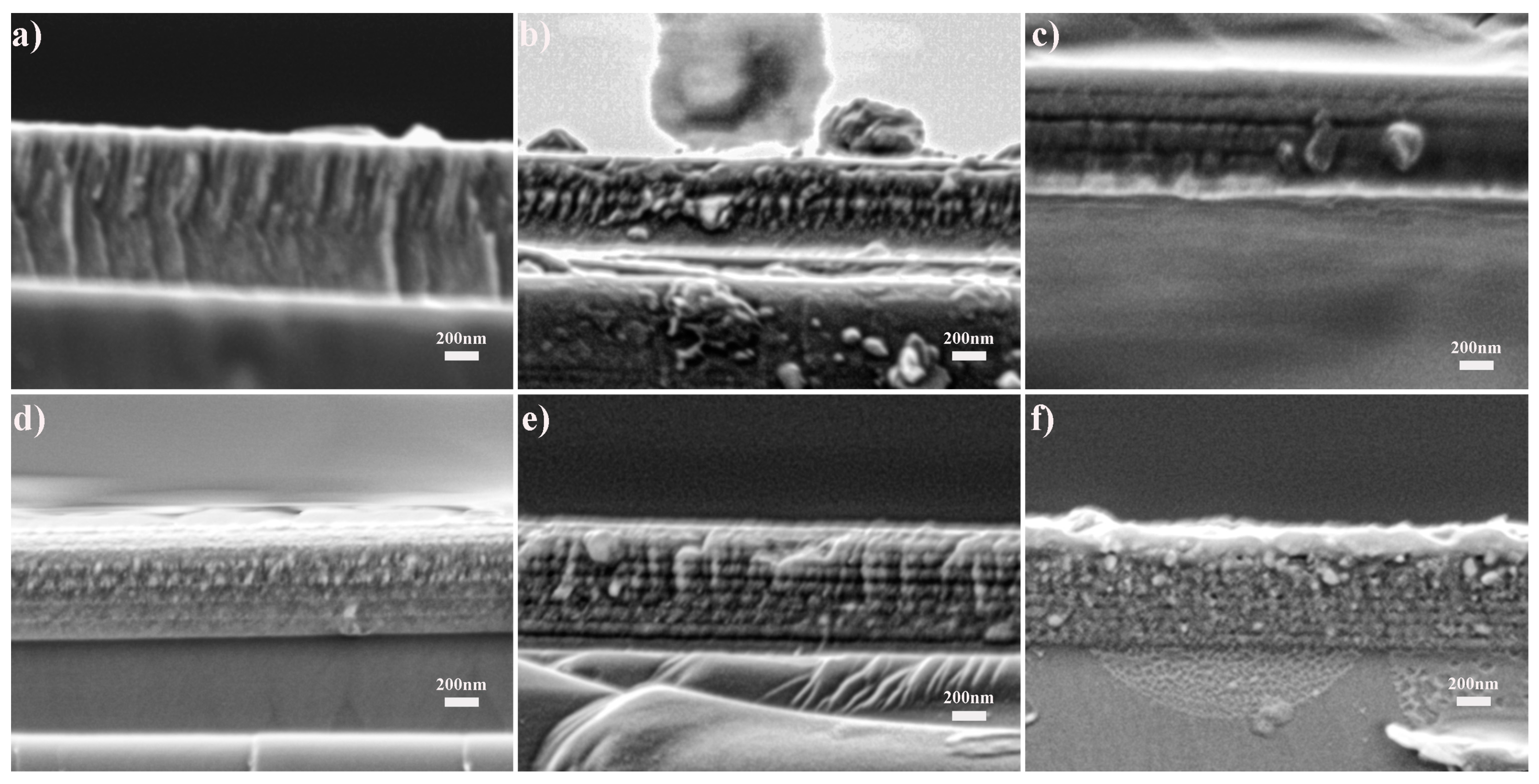
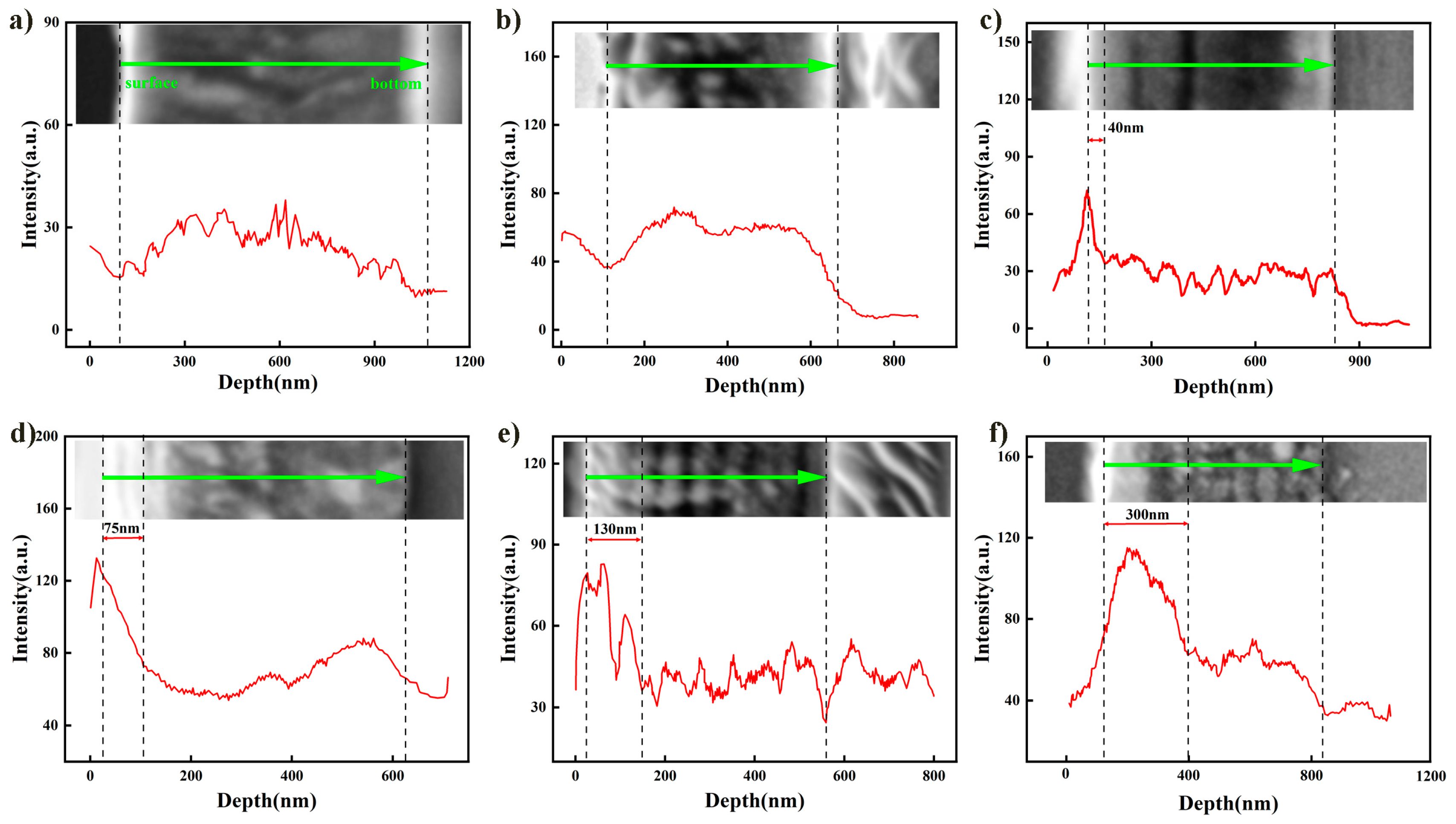
3.2. Oxidation of the Films

Figure 7 shows the XRD patterns of the Mo2N film, MoSi2 film, and Mo2N/MoSi2 multi-layer films after oxidation at different temperatures. Figure 7a shows the XRD pattern of the Mo2N film oxidized at 450 °C. The peaks corresponding to MoO3 (PDF #01-076-1003) are clearly observed, while the intensity of the diffraction peaks of Mo2N is almost negligible. This phenomenon indicates that the Mo2N film is severely oxidized at 450 °C. In contrast, the XRD pattern of the MoSi2 film oxidized at 600 °C shows only the characteristic diffraction peaks of MoSi2 (PDF #01-081-0167), with no peaks of oxidation products, indicating that MoSi2 is almost not oxidized at 600 °C. In this study, all MoSi2/Mo2N multi-layer films exhibit similar changes in oxidation resistance with increasing temperature. Therefore, the 20-layer film with the smallest thickness of the individual layer is used to demonstrate the temperature-dependent changes in oxidation resistance. Figure 7b shows the XRD patterns of the 20-layer Mo2N/MoSi2 film at various oxidation temperatures. At 450 °C, the diffraction peaks for Mo2N and MoSi2 are clearly discernible, and no characteristic peaks of MoO3 are detected, indicating a low level of oxidation in the 20-layer film at this temperature. In the XRD pattern of the 20-layer film at temperatures higher than 500 °C, peaks corresponding to MoO3, Mo2N (PDF #00-025-1366), and MoSi2 are identified. As the temperature increases, the intensity of the MoO3 diffraction peaks gradually increases, and the strongest diffraction peak of MoO3 notably reaches its maximum intensity at 550 °C. While the temperature increases to 600 °C, the intensity of the MoO3 diffraction peak decreases, which is possibly due to the high-temperature volatility of MoO3 [40]. This phenomenon indicates that the 20-layer Mo2N/MoSi2 films begin to oxidize above 500 °C, and the degree of oxidation increases with increasing temperature. Figure 7c exhibits the XRD patterns of Mo2N/MoSi2 multi-layer films with various layer numbers oxidized at 550 °C. For the 4-, 8-, and 12-layer films, diffraction peaks of MoSi2 and Mo2N are observed, while MoO3 peaks are undetectable, indicating that these films have strong oxidation resistance at 550 °C. The 16-layer film exhibits weak MoO3 peaks, indicating that the film was slightly oxidized. In contrast, the 20-layer film shows significantly strong MoO3 peaks, indicating that the film was severely oxidized. Nevertheless, the diffraction peaks of Mo2N remain visible, suggesting that Mo2N in the film still partially retains a structure that has not been completely oxidized. These results indicate that the Mo2N/MoSi2 multi-layer films significantly enhance oxidation resistance. However, the oxidation resistance of MoSi2/Mo2N multi-layer films decreases progressively with decreasing the thickness of the individual layer.
By comparing the phase structural alterations of the Mo2N/MoSi2 multi-layer films before and after oxidation, the possible oxidation reactions can be identified as follows:
M o 2 N   ( s ) + 3 O 2   ( g ) = 2 M o O 3   ( s ) + 1 2 N 2   ( g )
M o O 3   ( s ) = M o O 3   ( g )
To investigate the changes in the structure and morphology of the oxidized MoSi2/Mo2N multi-layer films, the surface and cross-sectional morphologies of the MoSi2 film and Mo2N/MoSi2 multi-layer films oxidized at 550 °C are displayed in Figure 8 and Figure 9, respectively. The surface morphologies of the MoSi2 film and 4-, 8-, and 12-layer Mo2N/MoSi2 films after oxidation are not significantly different from those before oxidation (Figure 2), as shown in Figure 8a–d. Figure 8e shows the grain boundary voids on the surface of the 16-layer film after oxidation. As shown in Figure 8f, the oxidized 20-layer film demonstrates a porous network structure, indicating that the film is severely oxidized.
Figure 9 shows the cross-sectional morphologies of the MoSi2 film and Mo2N/MoSi2 multi-layer films oxidized at 550 °C. In Figure 9a,b, the cross-sectional morphologies of the MoSi2 film and 4-layer film show little change compared to those before oxidation, except for a slightly smoother edge profile in the oxidized sample. In Figure 9c–e, the cross-sectional morphologies of the 8-layer, 12-layer, and 16-layer films underwent slight changes, although the inner layer boundaries remained visible. As shown in Figure 9f, the cross-sectional morphology of the 20-layer film underwent a significant change compared to that before oxidation. The interlayer interface became increasingly blurred from the bottom to the top, and the top four layers form a continuous monolithic structure. The columnar structure of the middle and lower layers of the 20-layer film was transformed into a granular structure. The cross-sectional morphologies of the oxidized films revealed that both the layer number and thickness of the individual layers of Mo2N/MoSi2 multi-layer films profoundly affect the oxidation resistance. As the thickness of the individual layer increases, the oxidation resistance of the multi-layer improves.
To quantitatively investigate the oxidation behavior of the MoSi2 film and Mo2N/MoSi2 multi-layer films, the oxygen distribution on the cross-section of the oxidized film, analyzed using EDS line scanning, is shown in Figure 10. In Figure 10a,b, the oxygen content curves of the MoSi2 film and the 4-layer film are smooth, and no obvious peaks are observed; this phenomenon indicates that the oxygen diffusion depth of the MoSi2 film and the 4-layer film is approximately 0. In Figure 10c–f, the oxygen diffusion depths of the 8-, 12-, 16-, and 20-layer films are approximately 40, 70, 130, and 300 nm, respectively. Based on Fick’s second law of one-dimensional diffusion [41]:
r 2 = 4 d t
where r is the diffusion depth (nm), d is the diffusion coefficient, and t is the experimental time (min). In this case, the diffusion time is 290 min for all films, where rn and dn represent the oxide thickness and diffusion coefficient of the films with different layer numbers, respectively. From Figure 10, the values of rMoSi2, r4, r8, r12, r16, and r20 are approximately 0, 0, 40, 70, 130, and 300 nm, respectively. According to Formula (4), dMoSi2, d4, d8, d12d16, and d20 can be calculated as 0, 0, 1.38, 4.23, 14.57, and 77.59 nm2/min, respectively. These results indicate that the diffusion velocity gradually increases with an increase in the number of layers.
Comprehensive XRD, FESEM, and EDS analyses indicate that Mo2N/MoSi2 multi-layer films can enhance the oxidation resistance of the Mo2N film. However, with an increasing number of layers, the thickness of the individual layer gradually decreases, and the oxidation resistance of the Mo2N/MoSi2 films declines. The oxidation resistance of Mo2N/MoSi2 multi-layer films is stronger than that of Mo2N, which can be explained in two ways. First, the MoSi2 layer on the surface of Mo2N/MoSi2 multi-layer films possesses excellent oxidation resistance [42]. Second, the interfacial structure between the multi-layer acts as a barrier layer, significantly impeding oxygen diffusion [43]. The degradation in the oxidation resistance of Mo2N/MoSi2 multi-layer films with an increasing number of layers is attributed to two primary mechanisms: First, when the number of layers is low, the thick MoSi2 surface layer effectively blocks the propagation of oxidation into the inner layers [44]. When the layer number is higher, pinhole defects on the surface of the films provide oxygen diffusion channels. Second, the volatilization of MoO3 creates voids that facilitate the inward propagation of oxidation through the inner layers [45,46].

3.3. Nanoindentation of the Films

Figure 11 shows the hardness (H) and elastic modulus (E) of the Mo2N/MoSi2 multi-layer films. In this study, the hardness and elastic modulus values were determined by averaging the values obtained in the 100–200 nm depth range, which effectively reduces the interference from surface roughness and substrate materials. In the 100–200 nm depth range, the number of layers corresponding to 4-, 8-, 12-, 16-, and 20-layer films is 1, 1–3, 2–4, 3–6, and 4–8 layers, respectively. To ensure data reliability, all specimens were subjected to multiple tests under identical experimental conditions, and the final results were obtained by averaging three valid measurements. The hardness improved from 21.65 ± 1.08 GPa in the 4-layer film (largest thickness of the individual layer) to 32.14 ± 1.38 GPa in the 20-layer film (smallest thickness of the individual layer). The Mo2N/MoSi2 multi-layer films achieved a hardness of 32 GPa, which is within the high range reported in the literature for other Mo2N-based multi-layer systems [16,47]. The improvement in the hardness of the Mo2N/MoSi2 multi-layer films can be attributed to the following factors: First, the hardness of the multi-layer films is primarily affected by the variation in the thickness of the individual layer. As the thickness of an individual layer decreases, the number of interlayer interfaces increases, leading to an increase in the film hardness [48,49]. Additionally, the variation in the thickness of the individual layer also affects the grain size, and the grain size of Mo2N and MoSi2 becomes progressively finer with decreasing thickness of the individual layer. In accordance with the Hall-Petch relationship [50], the hardness of the film increases with decreasing grain size when the grain size is below 100 nm [51]. The elastic modulus of the Mo2N/MoSi2 multi-layer films increased from 256.62 ± 7.04 GPa in the 4-layer film (the largest thickness of the individual layer) to 331.17 ± 9.59 GPa in the 20-layer film (the smallest thickness of the individual layer). This result demonstrates a clear correlation between the reduction in the thickness of the individual layers and the improvements in both the hardness and elastic modulus.
In addition to the trends in hardness and elastic modulus, the H/E and H3/E2 values were calculated to evaluate the tribological properties of the films. Leyland’s hypothesis suggests that the H/E and H3/E*2 ratios are associated with the tribological properties of the films, including durability, elastic strain resistance, and plastic deformation resistance [52,53]. The H/E ratio represents the elastic strain failure factor, with a higher value indicating a greater fracture resistance of the films. The H3/E*2 ratio represents the resistance to plastic deformation, where E* = E/(1 − ν2), here E is the elastic modulus and ν is Poisson’s ratio (ν = 0.25). A higher H3/E*2 value indicates that the film can withstand higher contact stress and offers better wear resistance [54,55]. Figure 12 shows the H/E and H3/E*2 values for different thicknesses of the MoSi2 individual layer. As the thickness of the MoSi2 individual layer decreases, the H/E values increases from 0.084 (thickness of MoSi2 individual film is 220 nm) to 0.098 (thickness of MoSi2 individual film is 71 nm) and then exhibited minor fluctuations, while the H3/E*2 values consistently increased from 0.136 (thickness of MoSi2 individual film is 220 nm) to 0.266 (thickness of MoSi2 individual film is 43 nm). This phenomenon indicates that as the thickness of the individual layer decreases, the increase in both H/E and H3/E*2 values will gradually enhance the wear resistance and fracture resistance of the Mo2N/MoSi2 multi-layer films [56].

4. Conclusions

Mo2N/MoSi2 multi-layer films are deposited on Si (100) and stainless steel substrates by reactive magnetron sputtering. The primary conclusions of this research are summarized as follows:
(1)
The Mo2N/MoSi2 multi-layer films consist of cubic Mo2N and hexagonal MoSi2 phases, and the average grain size decreases with decreasing thickness of the individual layer. The decrease in grain size is attributed to the confinement effect of the interlayer interfaces, which inhibits grain growth and refines the grain size.
(2)
The Mo2N/MoSi2 multi-layer films exhibit better oxidation resistance than the pure Mo2N films. This is primarily attributed to the superior oxidation resistance of the MoSi2 layer and the barrier effect of the multi-layer interfaces. However, as the number of layers increases and the thickness of the individual layers decreases, the pinhole defects on the surface of the films provide oxygen diffusion channels, leading to a gradual decline in the oxidation resistance of the film. Additionally, under high-temperature conditions, the degradation in the oxidation resistance of the multi-layer films may be attributed to the volatilization of the oxidation product MoO3, which creates channels for oxygen ingress.
(3)
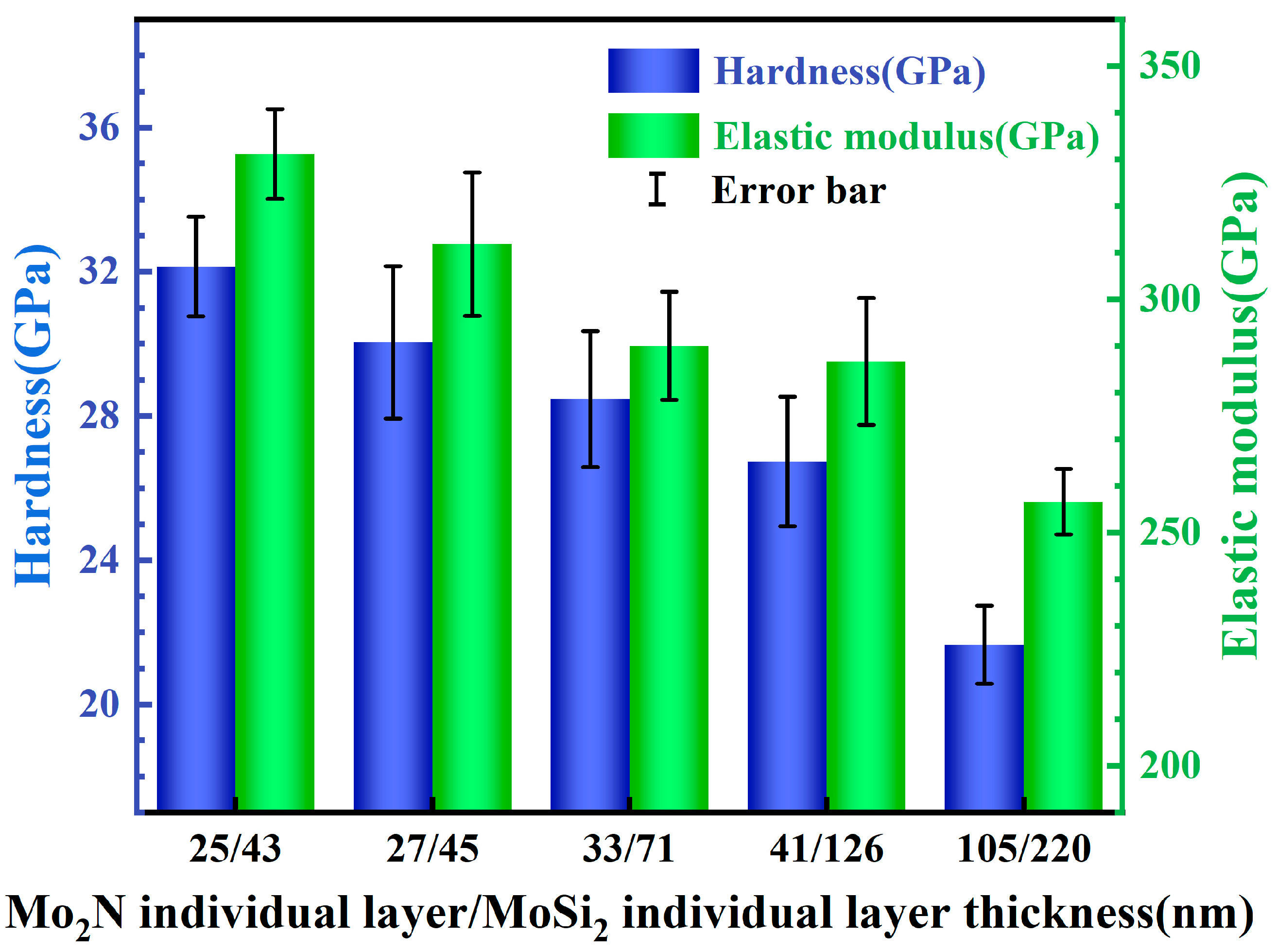
The Mo2N/MoSi2 multi-layer films exhibit higher elastic modulus and hardness than the MoSi2 and Mo2N films. The elastic modulus and hardness of the Mo2N/MoSi2 multi-layer films increase progressively with an increasing number of layers, which can be ascribed to the combined action of the reduction in the thickness of the individual layer, the increase in the interlayer interface, and grain refinement.
(4)
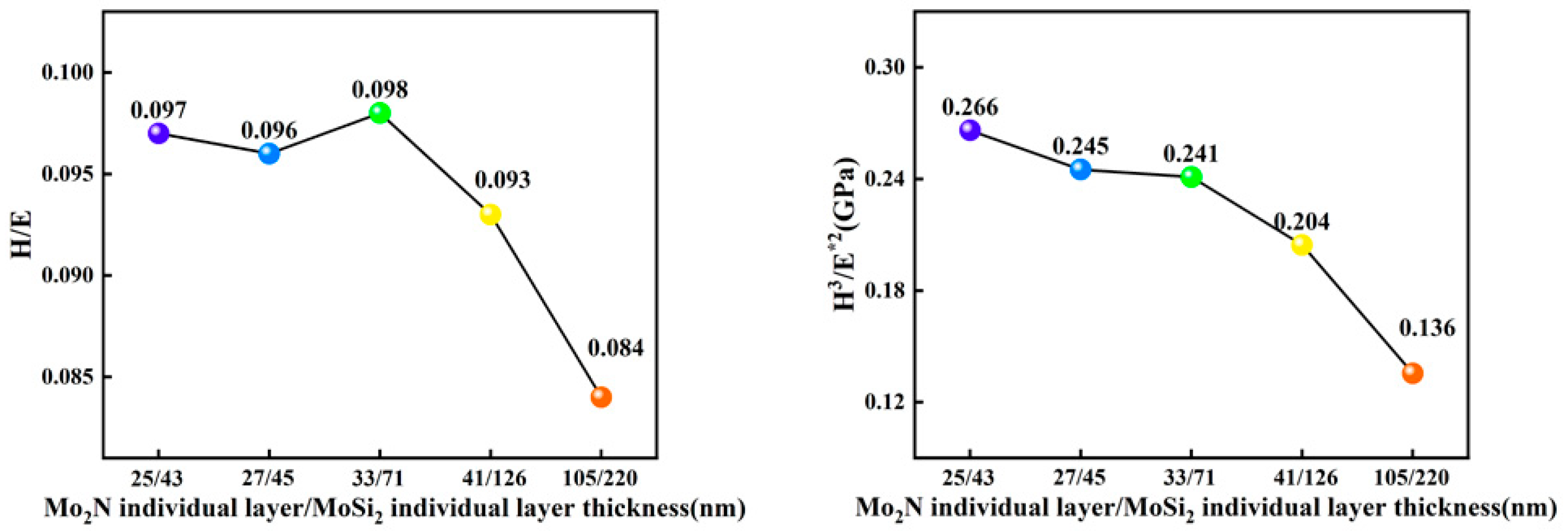
The H/E and H3/E*2 values of the 20-layer Mo2N/MoSi2 multi-layer film are relatively high, indicating that the 20-layer film has excellent tribological properties.

Author Contributions

Conceptualization, Z.Y. and L.S.; methodology, Z.Y. and G.Y.; software, Z.Y. and G.Y.; validation, Z.Y., L.S. and G.Y.; formal analysis, Z.Y., G.Y. and R.M.; investigation, S.M. and Z.C.; resources, Z.Y., L.S., J.Y., Y.L. and Q.F.; data curation, Z.Y., G.Y. and R.M.; writing—original draft preparation, Z.Y. and G.Y.; writing—review and editing, L.S. and Z.Y.; visualization, Y.L., Q.F. and J.Y.; supervision, L.S. and Y.L.; project administration, S.M. and Z.C.; funding acquisition, L.S. and Z.Y. All authors have read and agreed to the published version of the manuscript.

Funding

This work has been subsidized by the National Natural Science Foundation of China (Grant No. 11904268, U22B2066) and the Major Science and Technology Projects of Anhui Province (No. 202103a05020016).

Institutional Review Board Statement

Not applicable.

Informed Consent Statement

Not applicable.

Data Availability Statement

Data are contained within this article.

Conflicts of Interest

The authors declare no conflicts of interest.

References

  1. Xu, J.; Ju, H.; Yu, L. Influence of Silicon Content on the Microstructure, Mechanical and Tribological Properties of Magnetron Sputtered Ti-Mo-Si-N Films. Vacuum 2014, 110, 47–53. [Google Scholar] [CrossRef]
  2. Zhou, R.; Ju, H.; Liu, S.; Zhao, Z.T.; Xu, J.; Yu, L.; Qian, H.; Jia, S.; Song, R.; Shen, J. The Influences of Ag Content on the Friction and Wear Properties of TiCN-Ag Films. Vacuum 2022, 196, 110719. [Google Scholar] [CrossRef]
  3. Kindlund, H.; Sangiovanni, D.G.; Petrov, I.; Greene, J.E.; Hultman, L. A Review of the Intrinsic Ductility and Toughness of Hard Transition-Metal Nitride Alloy Thin Films. Thin Solid Films 2019, 688, 137479. [Google Scholar] [CrossRef]
  4. Zhang, X.; Tian, X.B.; Zhao, Z.W.; Gao, J.B.; Zhou, Y.W.; Gao, P.; Guo, Y.Y.; Lv, Z. Evaluation of the Adhesion and Failure Mechanism of the Hard CrN Coatings on Different Substrates. Surf. Coat. Technol. 2019, 364, 135–143. [Google Scholar] [CrossRef]
  5. Mei, H.; Cai, Z.; Ding, J.; Yan, K.; Li, Q.; Zhao, Z.; Gong, W. The Additions of V and Cu on the Microstructure and Mechanical Properties of Mo-N Coatings. Coatings 2022, 12, 1129. [Google Scholar] [CrossRef]
  6. Hao, J.; Zhang, K.; Ren, P.; Chen, J.; Wang, M.; Zhang, Y.; Wen, M. Tuning the Wettability, Mechanical and Tribological Properties of NbN Films by Doping Rare Earth Cerium. J. Alloys Compd. 2020, 814, 152339. [Google Scholar] [CrossRef]
  7. Sun, L.; Mao, J.H.; Li, Y.C.; Zhou, Q.; Yuan, Z.G.; Xiong, X.S.; Fang, Q.F.; Gong, W.B.; Lu, J.J.; Tang, L.B.; et al. Microstructures and Mechanical Properties of MoNx Isomeric Multilayer films with Different Number of Layers Deposited by DC Magnetron Sputtering. Materialia 2023, 28, 101714. [Google Scholar] [CrossRef]
  8. Krysina, O.V.; Ivanov, Y.F.; Koval, N.N.; Prokopenko, N.A.; Shugurov, V.V.; Petrikova, E.A.; Tolkachev, O.S. Composition, Structure and Properties of Mo-N Coatings Formed by the Method of Vacuum-Arc Plasma-Assisted Deposition. Surf. Coat. Technol. 2021, 416, 127153. [Google Scholar] [CrossRef]
  9. Wang, C.; Wang, Y.; Wu, X.; Li, X.; Luo, J. The Preparation and Superconducting Properties of Mo2N Nano Films by High Temperature Nitriding Method. Mater. Lett. 2021, 287, 129292. [Google Scholar] [CrossRef]
  10. Liu, C.; Ju, H.; Yu, L.; Xu, J.; Geng, Y.; He, W.; Jiao, J. Tribological Properties of Mo2N Films at Elevated Temperature. Coatings 2019, 9, 734. [Google Scholar] [CrossRef]
  11. Wang, T.; Zhang, G.J.; Liu, Z.N.; Jiang, B.L. Oxidation Behavior of Magnetron Sputtered Mo2N /AlN Multilayer Coatings During Heat Treatment. Ceram. Int. 2015, 41, 7028–7035. [Google Scholar] [CrossRef]
  12. Bouaouina, B.; Besnard, A.; Abaidia, S.E.; Haid, F. Residual Stress, Mechanical and Microstructure Properties of Multilayer Mo2N/CrN Coating Produced by RF Magnetron Discharge. Appl. Surf. Sci. 2017, 395, 117–121. [Google Scholar] [CrossRef]
  13. Cheng, W.J.; Wang, J.J.; Ma, X.; Liu, P.; Liaw, P.K.; Li, W. A Review on Microstructures and Mechanical Properties of Protective Nano-Multilayered Films or Coatings. J. Mater. Res. Technol. 2023, 27, 2413–2442. [Google Scholar] [CrossRef]
  14. Yuan, Z.G.; Li, Y.C.; Sun, L.; Yang, J.F.; Mei, S.Q.; Xiong, X.S.; Fang, Q.F.; Chen, Z.; Liu, Y. Microstructures and Tribological Properties of MoS2/ Mo2N Multilayer Gradient Films Deposited by Reactive Magnetron Sputtering. J. Mater. Res. Technol. 2024, 31, 1507–1517. [Google Scholar] [CrossRef]
  15. Gulbiński, W.; Suszko, T. Thin Films of Mo2N/Ag Nanocomposite—The Structure, Mechanical and Tribological Properties. Surf. Coat. Technol. 2006, 201, 1469–1476. [Google Scholar] [CrossRef]
  16. Ju, H.B.; Zhou, R.; Luan, J.; Yu, L.H.; Xu, J.H.; Zuo, B.; Yang, J.F.; Geng, Y.X.; Zhao, L.J.; Fernandes, F. Multilayer Mo2N-Ag/SiNx Films for Demanding Applications: Morphology, Structure and Temperature-Cycling Tribological Properties. Mater. Des. 2022, 223, 111128. [Google Scholar] [CrossRef]
  17. Ju, H.B.; Zhou, R.; Liu, S.J.; Yu, L.H.; Xu, J.H.; Geng, Y.X. Enhancement of the Tribological Behavior of Self-Lubricating Nanocomposite Mo2N/Cu Films by Adding the Amorphous SiNx. Surf. Coat. Technol. 2021, 423, 127565. [Google Scholar] [CrossRef]
  18. Lin, Z.X.; Liu, Y.C.; Huang, C.R.; Guillon, M.; Wu, F.B. Input Power Effect on Microstructure and Mechanical Properties of MoSiN Multilayer Coatings. Surf. Coat. Technol. 2020, 383, 125222. [Google Scholar] [CrossRef]
  19. Liang, B.H.; Hsieu, F.S.; Wu, F.B. Modulation Effect on Mechanical Properties of Nanolayered MoN/MoSiN Coatings. Surf. Coat. Technol. 2022, 436, 128278. [Google Scholar] [CrossRef]
  20. Leonov, A.A.; Denisova, Y.A.; Denisov, V.V.; Syrtanov, M.S.; Shmakov, A.N.; Savostikov, V.M.; Teresov, A.D. Structure and Properties of CrN/TiN Multi-Layer Coatings Obtained by Vacuum-Arc Plasma-Assisted Deposition Method. Coatings 2023, 13, 351. [Google Scholar] [CrossRef]
  21. Gao, Z.C.; Buchinger, J.; Koutná, N.; Wojcik, T.; Hahn, R.; Mayrhofer, P.H. Ab Initio Supported Development of TiN/MoN Superlattice Thin Films with Improved Hardness and Toughness. Acta Mater. 2022, 231, 117871. [Google Scholar] [CrossRef]
  22. Hahn, R.; Koutná, N.; Wójcik, T.; Davydok, A.; Kolozsvári, S.; Krywka, C.; Holec, D.; Bartosik, M.; Mayrhofer, P.H. Mechanistic Study of Superlattice-Enabled High Toughness and Hardness in MoN/TaN Coatings. Commun. Mater. 2020, 1, 62. [Google Scholar] [CrossRef]
  23. Schlögl, M.; Mayer, B.; Paulitsch, J.; Mayrhofer, P.H. Influence of CrN and AlN Layer Thicknesses on Structure and Mechanical Properties of CrN/AlN Superlattices. Thin Solid Films 2013, 545, 375–379. [Google Scholar] [CrossRef]
  24. Tian, C.X.; Xiang, Y.X.; Zou, C.W.; Yu, Y.J.; Abudouwufu, T.; Yang, B.; Fu, D.J. Mechanical and Tribological Properties of CrWN/MoN Nano-Multilayer Coatings Deposited by Cathodic Arc Ion Plating. Coatings 2024, 14, 367. [Google Scholar] [CrossRef]
  25. Wu, Z.T.; Ye, R.L.; Bakhit, B.; Petrov, I.; Hultman, L.; Greczynski, G. Improving Oxidation and Wear Resistance of TiB2 Films by Nano-Multilayering with Cr. Surf. Coat. Technol. 2022, 436, 128337. [Google Scholar] [CrossRef]
  26. Ren, S.M.; Cui, M.J.; Pu, J.B.; Xue, Q.J.; Wang, L.P. Multilayer Regulation of Atomic Boron Nitride Films to Improve Oxidation and Corrosion Resistance of Cu. ACS Appl. Mater. Interfaces 2022, 9, 27152–27165. [Google Scholar] [CrossRef]
  27. Li, Z.; Ma, G.Z.; Xing, Z.G.; Yong, Q.S.; Zhao, H.C.; Huang, Y.F.; Guo, W.L.; Zhang, Z.N.; Wang, H.D. The Effects of Cr and B Doping on the Mechanical Properties and Tribological Behavior of Multi-Layered Hydrogenated Diamond-Like Carbon Films. Surf. Coat. Technol. 2022, 431, 127977. [Google Scholar] [CrossRef]
  28. Martinez, E.; Sanjindopinges, R.; Karimi, A.; Esteve, J.; Lévy, F. Mechanical Properties of Nanocomposite and Multilayered Cr-Si-N Sputtered Thin Films. Surf. Coat. Technol. 2004, 180, 570–574. [Google Scholar] [CrossRef]
  29. Zhu, L.; Chen, P.; Cai, Z.M.; Feng, P.Z.; Kang, X.Q.; Akhtar, F.; Wang, X. Fabrication of MoSi2 Coatings on Molybdenum and Its High-Temperature Anti-Oxidation Properties. Trans. Nonferrous Met. Soc. China 2022, 32, 935–946. [Google Scholar] [CrossRef]
  30. Ren, X.R.; Lv, J.S.; Li, W.; Hu, Y.W.; Sun, K.; Ma, C.; Chu, H.A.; Wang, W.G.; Xu, L.H.; Li, Z.Y.; et al. Influence of MoSi2 on Oxidation Protective Ability of TaB2-SiC Coating in Oxygen-Containing Environments within a Broad Temperature Range. J. Adv. Ceram. 2020, 9, 703–715. [Google Scholar] [CrossRef]
  31. Liu, Y.Q.; Shao, G.; Tsakiropoulos, P. On the Oxidation Behaviour of MoSi2. Intermetallics 2001, 9, 125–136. [Google Scholar] [CrossRef]
  32. Isik, M.; Gasanly, N.M.; Rustamov, F.A. Determination of mechanical properties of Bi12TiO20 crystals by nanoindentation. Mater. Sci. Semicond. Process. 2022, 140, 106389. [Google Scholar] [CrossRef]
  33. McDonald, I.G.; Moehlenkamp, W.M.; Arola, D.; Wang, J. Residual Stresses in Cu/Ni Multilayer Thin Films Measured Using the Sin2ψ Method. Exp. Mech. 2019, 59, 111–120. [Google Scholar] [CrossRef]
  34. Cullity, B.D.; Stock, S.R. Elements of X-Ray Diffraction, 3rd ed.; Prentice-Hall: Upper Saddle River, NJ, USA, 2001; ISBN 0-201-61091-4. [Google Scholar]
  35. Bokuniaeva, A.O.; Vorokh, A.S. Estimation of Particle Size Using the Debye Equation and the Scherrer Formula for Polyphasic TiO2 Powder. J. Phys. Conf. Ser. 2019, 1410, 012057. [Google Scholar] [CrossRef]
  36. Anu, A.; Khadar, M.A. Charge transport in grain size tuned CuO nanocrystal films. J. Electroceram. 2020, 45, 15–21. [Google Scholar] [CrossRef]
  37. Mohamed, L.; Noureddine, M.; Mokhtar, B.; Al-Douri, J.; Djillali, B.; Lakhdar, B.; Abd El-Rehim, A.F.; Jadan, M. Dislocations and crystallite size distribution of cadmium oxide thin films synthesized by spray pyrolysis technique. Mater. Sci. Eng. B 2022, 286, 116055. [Google Scholar] [CrossRef]
  38. Caicedo, J.C.; Amaya, C.; Yate, L.; Gómez, M.E.; Zambrano, G.; Alvarado-Rivera, J.; Muñoz-Saldaña, J.; Prieto, P. TiCN/TiNbCN multilayer coatings with enhanced mechanical properties. Appl. Surf. Sci. 2010, 20, 5898–5904. [Google Scholar] [CrossRef]
  39. Gao, S.W.; Hu, Y.F. Simultaneously Higher Thermal Stability and Lower Resistance Drifting for Sb/In48.9Sb15.5Te35.6 Nanocomposite Multilayer films. CrystEngComm 2022, 24, 1638–1644. [Google Scholar] [CrossRef]
  40. Solak, N.; Ustel, F.; Urgen, M.; Aydin, S.; Cakir, A.F. Oxidation Behavior of Molybdenum Nitride Coatings. Surf. Coat. Technol. 2003, 174, 713–719. [Google Scholar] [CrossRef]
  41. Ellery, A.J.; Baker, R.E.; Simpson, M.J. Communication: Distinguishing between short-time non-Fickian diffusion and long-time Fickian diffusion for a random walk on a crowded lattice. J. Chem. Phys. 2016, 144, 171104. [Google Scholar] [CrossRef]
  42. Liu, L.; Zhang, H.Q.; Lei, H.; Li, H.Q.; Gong, J.; Sun, C. Influence of Different Coating Structures on the Oxidation Resistance of MoSi2 Coatings. Ceram. Int. 2020, 46, 5993–5997. [Google Scholar] [CrossRef]
  43. He, Y.X.; Wang, X.B.; Guo, T.; Gao, K.W.; Pang, X.L. Effect of Interface on Oxidation Behavior and Tribological Properties of CrAlN/SiNx multi-layer films. Ceram. Int. 2023, 49, 1369–1380. [Google Scholar] [CrossRef]
  44. Knittel, S.; Mathieu, S.; Vilasi, M. Oxidation Behaviour of Arc-Melted and Uniaxial Hot Pressed MoSi2 at 500 °C. Intermetallics 2010, 18, 2267–2274. [Google Scholar] [CrossRef]
  45. Fu, T.; Shen, F.Q.; Zhang, Y.Y.; Yu, L.H.; Cui, K.H.; Wang, J.; Zhang, X. Oxidation Protection of High-Temperature Coatings on the Surface of Mo-Based Alloys—A Review. Coatings 2022, 12, 141. [Google Scholar] [CrossRef]
  46. Abdollahi, A.; Ehsani, N.; Valefi, Z.; Khalifesoltani, A. SiC Nanoparticles Toughened-SiC/MoSi2-SiC Multilayer Functionally Graded Oxidation Protective Coating for Carbon Materials at High Temperatures. J. Mater. Eng. Perform. 2017, 26, 2878–2889. [Google Scholar] [CrossRef]
  47. Beltrami, M.; Mavrič, A.; Dal Zilio, S.; Kapun, G. A comparative study of nanolaminate CrN/Mo2N and CrN/W2N as hard and corrosion resistant coatings. Surf. Coat. Technol. 2023, 455, 129209. [Google Scholar] [CrossRef]
  48. Yuan, Z.G.; Mao, J.H.; Li, Y.C.; Sun, L.; Yang, J.F.; Fang, Q.G.; Gong, W.B.; Xiong, X.S.; Su, G.B. The Oxidation Resistance and Mechanical Properties of MoNx/AlN Multilayer Gradient Films Prepared by Magnetron Sputtering. J. Alloys Compd. 2024, 976, 172989. [Google Scholar] [CrossRef]
  49. Liu, H.H.; Yan, J.X.; Pei, Z.L.; Gong, J.; Sun, C. Effects of Mo Content on the Grain Size, Hardness and Anti-Wear Performance of Electrodeposited Nanocrystalline and Amorphous Ni-Mo Alloys. Surf. Coat. Technol. 2020, 404, 126476. [Google Scholar] [CrossRef]
  50. Hansen, N. Hall–Petch Relation and Boundary Strengthening. Scr. Mater. 2004, 51, 801–806. [Google Scholar] [CrossRef]
  51. Kariper, İ.A. Hardness of Mn2V2O7 Thin Films and Its Influential Factors. Int. J. Miner. Metall. Mater. 2015, 22, 987–991. [Google Scholar] [CrossRef]
  52. Leyland, A.; Matthews, A. On the Significance of the H/E Ratio in Wear Control: A Nanocomposite Coating Approach to Optimised Tribological Behaviour. Wear 2000, 246, 1–11. [Google Scholar] [CrossRef]
  53. Beake, B.D. The Influence of the H/E Ratio on Wear Resistance of Coating Systems–Insights from Small-Scale Testing. Surf. Coat. Technol. 2022, 442, 128272. [Google Scholar] [CrossRef]
  54. Shugurov, A.; Panin, A.; Dmitriev, A.; Nikonov, A. The Effect of Crystallographic Grain Orientation of Polycrystalline Ti on Ploughing Under Scratch Testing. Wear 2018, 408, 214–221. [Google Scholar] [CrossRef]
  55. Shtanskii, D.V.; Kulinich, S.A.; Levashov, E.A.; Moore, J.J. Structure and Physical-Mechanical Properties of Nanostructured Thin Films. Phys. Solid State 2003, 45, 1177–1184. [Google Scholar] [CrossRef]
  56. Pshyk, A.V.; Coy, L.E.; Nowaczyk, G.; Kempiński, M.; Peplińska, B.; Pogrebnjak, A.D.; Beresnev, V.M.; Jurga, S. High Temperature Behavior of Functional TiAlBSiN Nanocomposite Coatings. Surf. Coat. Technol. 2016, 305, 49–61. [Google Scholar] [CrossRef]
Figure 1. Schematic diagram of Mo2N/MoSi2 multi-layer films.
Coatings 15 00457 g001
Figure 2. The surface morphologies of MoSi2 film and Mo2N/MoSi2 multi-layer films: (a) MoSi2, (b) 4-layer, (c) 8-layer, (d) 12-layer, (e) 16-layer, (f) 20-layer.
Coatings 15 00457 g002
Figure 3. The cross-section morphologies of MoSi2 film and Mo2N/MoSi2 multi-layer films: (a) MoSi2, (b) 4-layer, (c) 8-layer, (d) 12-layer, (e) 16-layer, (f) 20-layer.
Coatings 15 00457 g003
Figure 4. XRD patterns of different films: (a) Mo2N film and MoSi2 film, (b) Mo2N/MoSi multi-layer films and the grain sizes of Mo2N and MoSi2 in the multi-layer films: (c) Mo2N, (d) MoSi2.
Coatings 15 00457 g004
Figure 5. Elemental content of pure MoSi2 film tested by EDS.
Coatings 15 00457 g005
Figure 6. The 3D surface topographies of MoSi2 film and Mo2N/MoSi2 multi-layer films: (a) MoSi2, (b) 4-layer, (c) 8-layer, (d) 12-layer, (e) 16-layer, (f) 20-layer.
Coatings 15 00457 g006
Figure 7. XRD patterns of oxidized films: (a) pure Mo2N film oxidized at 450 °C and pure MoSi2 film oxidized at 600 °C, (b) 20-layer Mo2N/MoSi2 multi-layer film oxidized at different temperatures, (c) Mo2N/MoSi2 multi-layer films with different layer number oxidized at 550 °C.
Coatings 15 00457 g007
Figure 8. The surface morphologies of MoSi2 film and Mo2N/MoSi2 multi-layer films oxidized at 550 °C: (a) MoSi2, (b) 4-layer, (c) 8-layer, (d) 12-layer, (e) 16-layer, (f) 20-layer.
Coatings 15 00457 g008
Figure 9. The cross-section morphologies of MoSi2 film and Mo2N/MoSi2 multi-layer films oxidized at 550 °C: (a) MoSi2, (b) 4-layer, (c) 8-layer, (d) 12-layer, (e) 16-layer, (f) 20-layer.
Coatings 15 00457 g009
Figure 10. EDS line scans of oxygen content in the cross-section of MoSi2 film and Mo2N/MoSi2 multi-layer films: (a) MoSi2, (b) 4-layer, (c) 8-layer, (d) 12-layer, (e) 16-layer, (f) 20-layer.
Coatings 15 00457 g010
Figure 11. Hardness and elastic modulus of Mo2N/MoSi2 multi-layer films.
Coatings 15 00457 g011
Figure 12. H/E and H3/E*2 ratio of Mo2N/MoSi2 multi-layer films.
Coatings 15 00457 g012
Table 1. Deposition parameter of different films.
Deposition Parameters Mo2NMoSi2
Mo/Si Sputter Power (W) 8080/100
N2/Ar Flow Rate (sccm) 10/200/25
Deposition Temperature (°C) 450
Working Pressure (Pa) 0.78
Deposition Time per Layer (s)pure Mo2N7200-
pure MoSi2-7200
4-layer18001800
8-layer900900
12-layer600600
16-layer450450
20-layer360360
Disclaimer/Publisher’s Note: The statements, opinions and data contained in all publications are solely those of the individual author(s) and contributor(s) and not of MDPI and/or the editor(s). MDPI and/or the editor(s) disclaim responsibility for any injury to people or property resulting from any ideas, methods, instructions or products referred to in the content.

