Article

Morphological, Compositional and Optical Properties of CuxS Films on FTO Glass

by
Dominyka Zubrickaite
,
Asta Bronusiene
and
Ingrida Ancutiene
*
Department of Physical and Inorganic Chemistry, Kaunas University of Technology, Radvilenu Str. 19, LT-50254 Kaunas, Lithuania
*
Author to whom correspondence should be addressed.
Coatings 2025, 15(10), 1221; https://doi.org/10.3390/coatings15101221
Submission received: 25 September 2025 / Revised: 10 October 2025 / Accepted: 16 October 2025 / Published: 17 October 2025

Abstract

In this study, by varying the concentrations of the precursors used, copper sulfide films were deposited on FTO glass using the sequential ionic layer adsorption and reaction (SILAR) method and the following copper sulfide phases were detected: anilite, djurleite, chalcocite, and yarrowite. It was found that the films of copper sulfides are unevenly distributed, that the crystallinity of the films increases with increasing annealing temperature from 100 to 400 °C, and that the particles aggregate into agglomerates. The films formed were found to be dominated by copper sulfides, and the calculated molar ratio of copper to sulfur varied with the concentrations of the precursors used, ranging from 1.4 to 2.2. The values of the band gap energy were not significantly affected by the change in the concentrations of the precursors and the annealing temperature, varying between 1.0 and 1.5 and 1.95–2.15 eV.

1. Introduction

The growing global demand for energy, coupled with concerns over fossil fuel depletion and environmental pollution, has intensified the search for alternative, sustainable, and low-emission energy sources. Among the materials being explored, copper sulfides (Cu2−xS) have attracted significant interest due to their favorable optical, electrical, and thermoelectric properties, as well as their abundance, low toxicity, and cost-effectiveness [1,2,3,4,5,6,7].
Copper sulfides are promising candidates for applications such as lithium-ion batteries, solar cells, thermoelectric devices, and other optoelectronic systems. With band gap energies ranging from 0.6 to 2.35 eV, their semiconducting nature makes them suitable for a variety of energy-related applications [1,8,9]. Compared to copper oxides, copper sulfides exhibit higher electrical conductivity and greater theoretical capacities as electrode materials (e.g., ~335 mAh/g for Cu2S and ~560 mAh/g for CuS) [3,10]. However, issues such as rapid capacity fading and limited active material utilization have hindered their broader application [10]. To overcome these limitations, researchers have explored morphological tuning (e.g., nanotubes, nanofibers, hollow spheres) and composite formation with conductive polymers or carbon-based materials to enhance electrochemical performance [10,11].
Copper sulfides exist in multiple stoichiometries—from copper-rich chalcocite (Cu2S) and djurleite (Cu1.95S) to sulfur-rich covellite (CuS)—each with distinct crystal structures and phase stability depending on temperature and synthesis method [12]. Owing to intrinsic copper vacancies, these materials typically behave as p-type semiconductors. Their high electrical conductivity and low thermal conductivity have also made them candidates for thermoelectric applications, with reported figures of merit (zT) as high as 1.9 at 970 K for dense Cu2−xS compositions [13].
In addition to energy storage and conversion, copper sulfides have been investigated for their optical and electronic properties in light-harvesting, photocatalysis, and sensor applications [6,7]. Morphology-dependent changes in band gap energy, for instance, in CuS microspheres (~2.06 eV), nanoparticles (~1.88 eV), and nanotubes (~2.06 eV), enable efficient absorption in the UV-visible range [14]. CuS nanostructures also exhibit photoluminescence, with blue emission around 465 nm, making them attractive for optoelectronic applications [14]. However, the direct relevance of optical absorption to gas sensing and conductive film performance remains underexplored.
Despite extensive study, the relationship between synthesis conditions, phase composition, and the resulting properties of copper sulfide thin films, especially for applications in optoelectronics and photocatalysis, remains insufficiently understood. The aim of the present work was to synthesize and characterize CuxS thin films deposited on FTO substrates using a sequential ionic layer adsorption and reaction method, a low-cost and accessible technique commonly employed for chalcogenide film fabrication. The effects of precursor concentrations and annealing on the films’ structural, morphological, and optical properties were systematically investigated. Characterization techniques included X-ray diffraction (XRD), scanning electron microscopy with energy-dispersive X-ray spectroscopy (SEM/EDS), and UV-Vis spectroscopy.
Despite extensive research, the relationship between synthesis conditions, phase composition, and the resulting properties of copper sulfide thin films, especially for optoelectronics and photocatalysis applications, is still not sufficiently investigated.

2. Materials and Methods

Materials. Copper sulfate pentahydrate (CuSO4 × 5H2O) (99.5% purity) and hydroquinone (C6H4(OH)2) (99%) were received from Labochema.com. Sodium sulfide nonahydrate (Na2S × 9H2O) (98%) was supplied by Honeywell.com. As the substrate, the fluorine-doped tin oxide (FTO) glass slides measuring 20 mm × 15 mm with a measured sheet resistance of 9.38 ± 0.38 Ω/sq were provided by Ossila.com.
Formation of CuxS films on FTO glass slides. A very important criterion is the preparation of the substrate. To ensure the optimal contact and favorable interaction between deposited film and substrate, FTO surface should be cleaned of any possible contaminants such as organic impurities, adventitious carbons, and dust particles [15]. In addition, surface contaminants may affect the film delamination at a later stage.
The preparation of the FTO glass substrates started with cleaning with soap and rinsing with water, followed by sonicating in acetone for 10–15 min. After this, the substrates were washed with distilled water and dried in air. The growth of copper sulfides films on FTO glass slides was carried out using the SILAR method. Copper sulfate solution with a reducing agent hydroquinone, which led to the change of Cu2+ to Cu+, was used as a cationic precursor. Sodium sulfide solution was used as an anionic precursor. For the deposition of copper sulfides, 40 °C solutions were applied.
Prepared glass slides were immersed in a cationic precursor solution for 30 s, then in anionic precursor solution for 30 s. Following immersion in the anionic precursor, the films were rinsed in distilled water to remove the excess of the precursors. After rinsing in distilled water, the substrate was immersed in cationic precursor solution and the SILAR deposition cycle began. The experimental steps are schematically illustrated in Figure 1.
Thin copper sulfide films on the FTO glass slides were formed by the following reaction:
2Cu+ + Cu2+ + 2S2− → Cu2S + CuS.
Annealing of samples. After the deposition, samples were placed for 1 h annealing in air in a muffle furnace SNOL-6.7/1300 (SnolTherm, Utena, Lithuania) at temperatures 100 °C, 200 °C, 300 °C, and 400 °C. After the annealing, the samples were cooled and used for following measurements.
The numbering of the samples and the concentrations of the precursors are given in Table 1.
XRD characterization. X-ray diffraction analysis of CuxSy films was carried out using a D8 Advance diffractometer (Bruker AXS, Karlsruhe, Germany). Operating voltage and current in the tubes of the device were 40 kV and 40 mA. To record diffraction patterns in the Bragg–Brentano geometry, a fast-counting one-dimensional Bruker LynxEye detector (Bruker AXS, Karlsruhe, Germany) based on silicon strip technology was used. The X-ray was filtered through a 0.02 mm Ni filter to suppress Cu-k alpha radiation, and the samples were scanned in the 2θ = 5–70° range at a scan rate of 1°/1 min−1. The diffractometer is supplied together with the software package DIFFRAC.SUITETM (Diffract. EVA. v. 4.5, Bruker AXS, Karlsruhe, Germany). X-ray diffractograms of formed films were processed using the software packages Crystallographica Search-Match v. 2.1, ConvX v.1.0, and Microsoft Office Excel.
SEM/EDS characterization. The surface structure and morphology of the samples were analyzed using a Hitachi S-3400N (Chiyoda, Tokyo, Japan) scanning electron microscope (SEM) with an IR CCD camera and high-quality secondary and backscattered electron detectors optimized for low vacuum. A Bruker Quad 5040 detector (Bruker AXS Microanalysis GmbH, Berlin, Germany) was used for energy-dispersive spectroscopy (EDS).
UV-Vis spectroscopy analysis. UV-Vis spectra were recorded at room temperature on a PerkinElmer Lambda 35 UV/VIS Spectrometer (Waltham, MA, USA) with The Labsphere RSA-PE-20 Diffuse Reflectance Sphere (LABSPHERE, INC., North Sutton, NH, USA) with compensation of the absorption of PA 6 sheet in the range of 200–1100 nm.

3. Results and Discussion

3.1. XRD Analysis

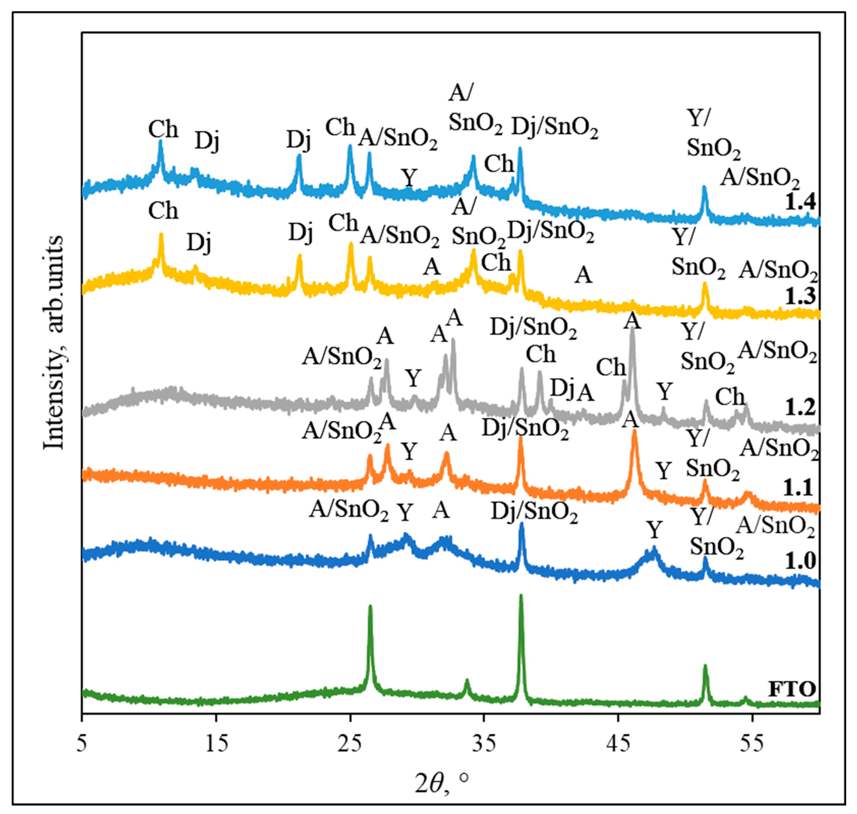
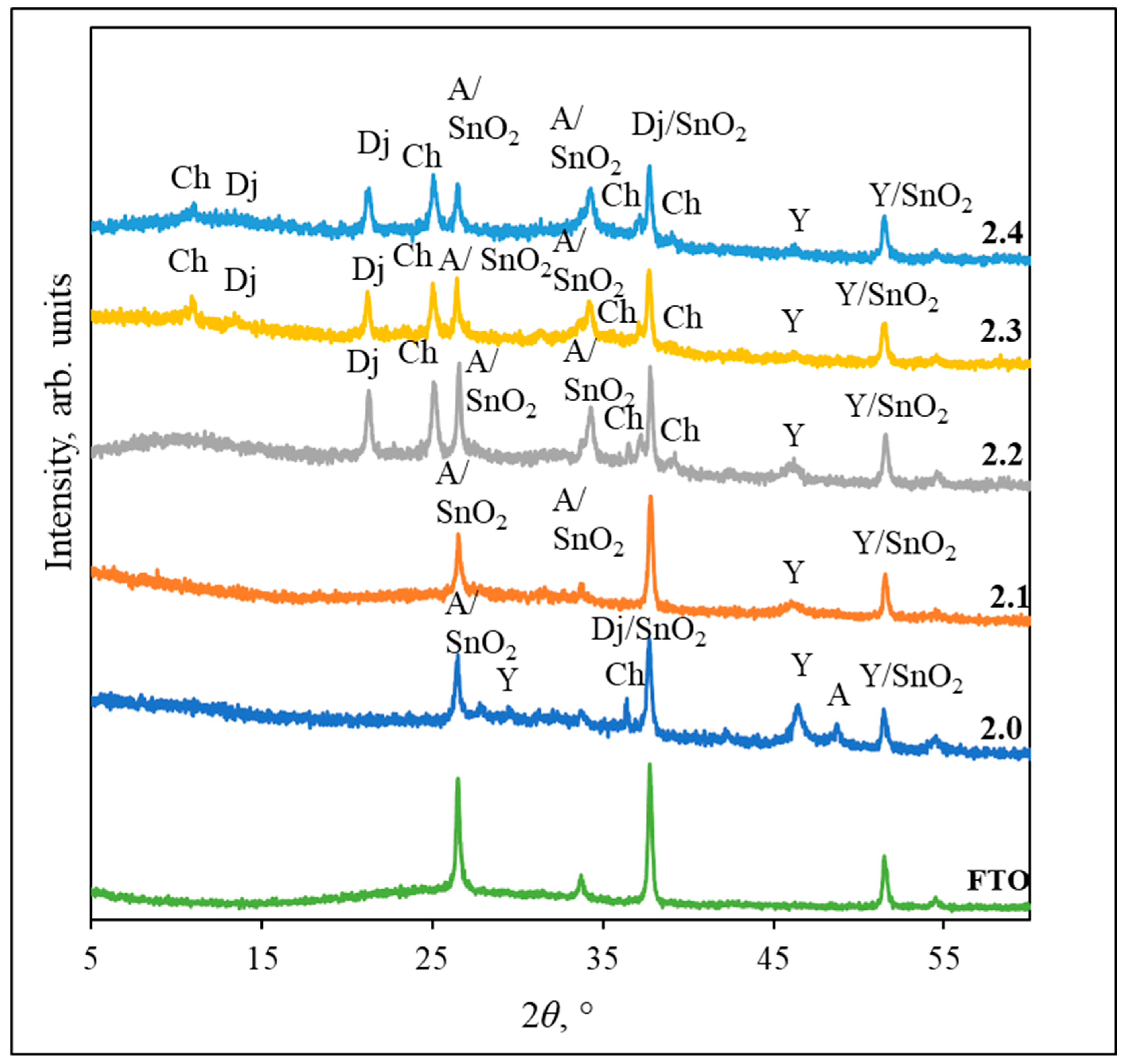
X-ray diffraction analysis was applied to the structural characterization of the obtained films and the results are given in Figure 2, Figure 3 and Figure 4. The XRD patterns of copper sulfides films obtained from all experiments correspond to a mixture of orthorhombic anilite (ICDD PDF no. 72-0617), hexagonal and orthorhombic chalcocite (JCPDS PDF no. 84-0207 and 12-0227), monoclinic djurleite (JCPDS PDF no. 42-0564), and hexagonal yarrowite (JCPDS PDF no. 36-0379) phases, as illustrated in Figure 2, Figure 3 and Figure 4. Copper sulfides (CuxS) in the obtained films vary from copper-rich phases including chalcocite (Cu2S), djurleite (Cu31S16 or Cu1.9375S), and anilite (Cu7S4 or Cu1.75S) to the copper-poor phase yarrowite (Cu9S8 or Cu1.125S). It can be seen that as-deposited samples (1.0, 2.0, and 3.0) consist mainly of anilite, djurleite, and yarrowite.
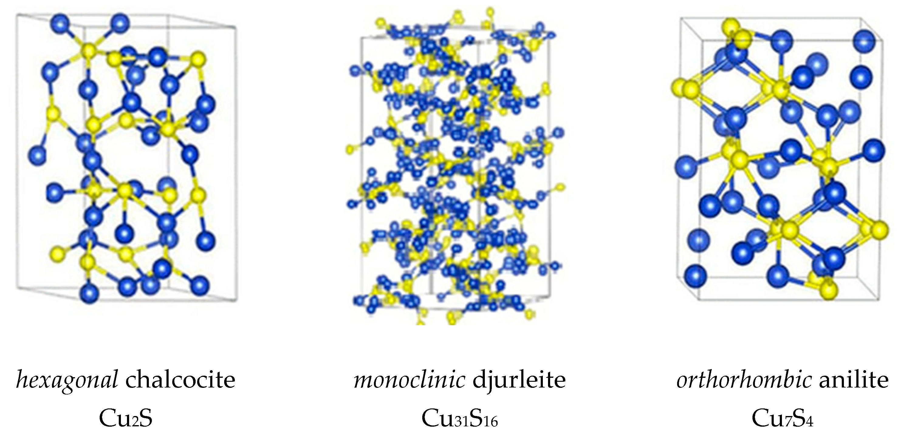
Since the position of Cu atoms in the close-packed S lattice varies with x, CuxS (1 ≤ x ≤ 2) has many crystal forms and can have cubic, hexagonal, orthorhombic, and monoclinic packing [10]. In Figure 2, crystal forms of some CuxS phases are presented.
Figure 3, Figure 4 and Figure 5 show the diffractogram of FTO glass, in which five peaks can be seen at 2θ = 26.60; 33.72; 37.86; 51.67; and 54.81°, corresponding to SnO2 (JCPDS PDF no. 46-1088) on the glass surface. The data in Figure 3 represents the results of samples prepared using 0.2 M CuSO4 solution with 0.2 M hydroquinone and 0.2 M Na2S. These conditions facilitate more amorphous films formation (Figure 3, curve 1.0). There are two peaks at 2θ = 26.55 and 32.13° (the interplanar spacings d are 3.3551 and 2.7832 Å), which match to the anilite phase, as well as three peaks with the broadening of the yarrowite phase at 2θ = 29.10, 47.60, and 51.40° (d = 3.0663, 1.9089, and 1.7761 Å). The most intensive peak at 2θ = 37.77° (d = 2.3799 Å) belongs to djurleite, but this peak could also be attributed to the SnO2, which is on top of the glass slide, and to the fact that the background of the FTO mirroring is not masked. Other intensive peaks with a similar situation are at 2θ = 26.55 and 51.40°, where anilite and yarrowite overlap with SnO2.
Annealing of the samples led to the formation of more copper sulfide phases, and different annealing temperatures affect this. Also, increasing the heating temperature improves the crystallinity of the films and intensifies the peaks of copper sulfides. Lower temperatures (100 and 200 °C) improve the growth of anilite [16,17], while higher temperatures (300 and 400 °C) increase the formation of chalcocite and djurleite [18,19]. After annealing the samples at low temperatures, it can be observed that the composition of the films changes slightly. The diffraction patterns of samples heated at 100 and 200 °C (1.1 and 1.2) show better intensity peaks of the anilite phase at 2θ = 26.55, 27.80, 32.13, and 46.25° and the djurleite phase at 2θ = 37.77°. With increasing temperature, the amount of the yarrowite phase decreases slightly, which, possibly due to diffusion processes in the film and phase transformations, transforms into the most stable anilite phase:
5Cu1.125S (yarrowite) + 18Cu1.9375S (djurleite) → 23Cu1.75S (anilite).
With a further increase in the annealing temperature to 300 °C and then to 400 °C, the presence of CuxS phases with high x value (chalcocite and djurleite) were observed due to the loss of sulfur in the form of sulfur dioxide, which evaporates and reacts with atmospheric oxygen [20]. The phase composition of the samples heated at temperatures of 300 and 400 °C (1.3 and 1.4) is similar; the peaks of djurleite, chalcocite, and anilite phases are predominant in these diffractograms. In the X-ray diffraction patterns of samples heated at 300 and 400 °C, another intensive peak of the djurleite phase appears at 2θ = 21.25° (d = 4.1786 Å), and two intensive peaks assigned to the chalcocite phase appear at 2θ = 10.89 and 25.05° (d =8.4939 and 3.5517 Å). Similarly to the previous results, there are also some peaks where CuxS overlaps with the SnO2 that is on top of the glass.
Figure 4 represents results of samples prepared using 0.2 M CuSO4 solution with 0.2 M hydroquinone and 0.1 M Na2S, where more crystalline patterns were observed. It can be seen that CuxS phases with a higher x value predominate in the films when a lower concentration sodium sulfide solution is used for the film formation. The X-ray diffraction pattern of the as-deposited film (2.0) shows less yarrowite phase, as only two more intensive yarrowite peaks are observed at 2θ = 29.10 and 51.40°. The sample is dominated by the peaks of the anilite phase and an intensive peak of the djurleite phase at 2θ = 37.77°. It can be noticed that the X-ray pattern of the film annealed at 100 °C (2.1) differs slightly from the diffractogram of the as-deposited film. The X-ray diffraction patterns (2.2, 2.3 and 2.4) of the samples annealed at 200, 300, and 400 °C are similar in composition, and the same abundant peaks of the anilite phase, a yarrowite phase peak at 2θ = 51.40°, two intensive djurleite phase peaks at 2θ = 21.25 and 37.77°, and an intensive peak at 2θ = 25.05° assigned to chalcocite can be observed in them. There are also some peaks where anilite, djurleite, and yarrowite overlap with the SnO2 that is on the surface of the FTO glass.
The composition of copper sulfide films prepared using a 0.2 M CuSO4 solution, but with a lower concentration (0.1 M) of hydroquinone and 0.2 M solution of Na2S, is presented in Figure 5. Peaks of the anilite, yarrowite, and djurleite phases are observed in the X-ray diffraction pattern of the as-deposited films (3.0). The lower concentration of hydroquinone significantly affects the formation of anilite, as fewer low-intensity peaks are observed in the diffraction pattern.
In the X-ray diffraction patterns of the heated samples at 100 and 200 °C (3.1 and 3.2), the same peaks of the anilite, djurleite, and yarrowite phases are observed as in the unannealed sample. In the diffractogram of sample 3.2, peaks of the chalcocite phase also appear at 2θ = 39.12 and 45.43° (d = 2.3008 and 1.9948 Å). In the X-ray diffraction patterns of samples 3.3 and 3.4 annealed at high temperatures (300 and 400 °C), more peaks of chalcocite and djurleite phases were detected. The figure shows very intensive peaks of the djurleite phase at 2θ = 21.25 and 37.77° and the chalcocite phase at 2θ = 10.89 and 25.05°.
Summarizing the X-ray diffraction patterns of the samples, it can be stated that with an increase in heating temperature, phase peaks of higher intensity and separation of peaks are observed. Based on the data presented in Figure 3, Figure 4 and Figure 5, it can be said that some of the peaks of anilite, djurleite, and yarrowite phases are in very similar locations to the peaks of SnO2 and overlap with one other.
Having assessed the results obtained, it can be concluded that the phase composition of copper sulfide films is influenced by both the concentration of the precursors used and the heating temperature of the samples.

3.2. SEM and EDS Analysis

The surface morphology of the copper sulfide films as deposited and annealed at different temperatures was investigated using SEM.
CuxS particles grow forming thin films on FTO glass slides and are well adhered to the substrate. As evident from the SEM images in Figure 6, the concentration of the solutions used affects the growth of the particles and the compactness of the obtained films. The deposited copper sulfide films consist of spherical particles that are not uniform in size, form clusters with voids and pinholes, and have a layered structure. These images show CuxS nanoparticles that are connected to each other to form dendrites.
The image shows that the film of sample 1.0 has an irregular morphology consisting of nanoparticle clusters that are densely packed. CuxS particles range in size between 150 and 500 nm. There are also deep voids visible, so the deposited film is not uniform. The film of sample 2.0 is very uneven, with visible deep voids and pinholes, so there may be uncovered areas of the substrate. Here it is clearly visible that copper sulfide forms irregularly shaped particles, and their size ranges from 120 to 400 nm. The surface morphology of the sample 3.0 changes to a more homogeneous one as the nanograins decrease in size (100–250 nm), but the film still has small voids.
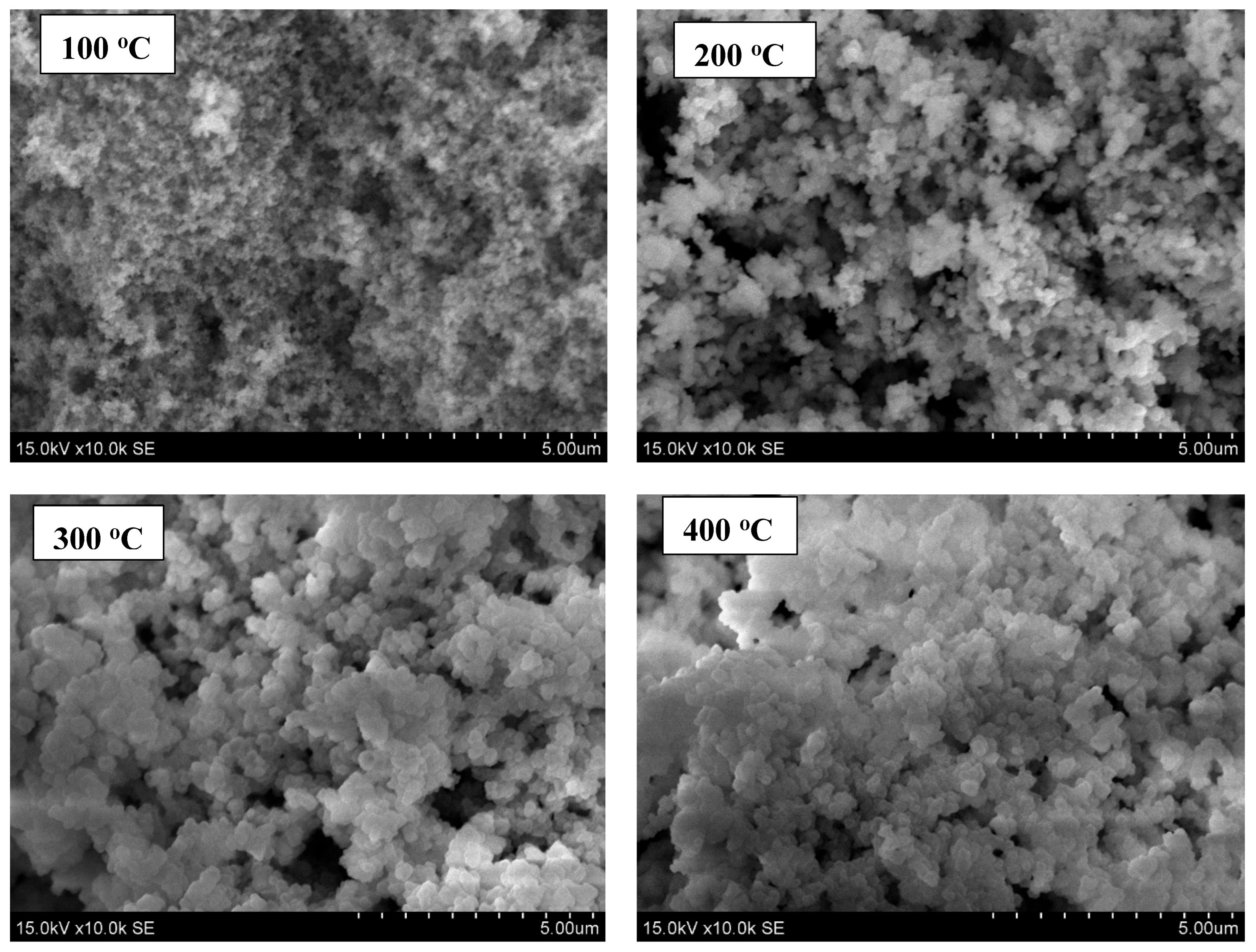
SEM analysis clearly demonstrates that annealing has a significant effect on particle size and surface roughness (Figure 7). At low annealing temperature (sample 1.1) copper sulfide nanoparticles with various sizes (110–250 nm) combined into big agglomerates. The film becomes more uniform and denser with formed clusters, so the surface does not look so deep. The annealing of the sample at 100 °C improved the morphology and compactness of the film. With increasing annealing temperature, the fragmentation of agglomerates increases. In the image of sample 1.2, it can be seen that the CuxS particles are in a range of 140–350 nm and the film contains deep voids. After increasing the annealing temperature to 300 °C, the nanoparticles turn into larger, well-packed agglomerates. The film of sample 1.3 is more homogeneous with spherical nanocrystalline grains in a range of 200–400 nm. On further annealing of the films at 400 °C, the CuxS grains agglomerate significantly and the surface of sample 1.4 is coated by tightly packed spherical grains with a size between 220 and 500 nm. Due to the observable agglomeration of nanoparticles, the film becomes the most uniform, as the particles merge into big clusters. As evident from the SEM images, as the annealing temperature increases, the particle size also increases.
The elemental composition of the as-deposited (1.0, 2.0 and 3.0) CuxS films determined using EDS analysis was studied. EDS spectra show that the copper peaks are dominant, and the sulfur peak is also very intense. It was observed that all spectra also contain oxygen peaks, but there are no tin or silicon peaks in the EDS spectra, which means that the oxides of these elements are not detected, so it is quite likely that oxygen adsorbed from the air may be present in the voids and pinholes between the dendrites. The spectrum of sample 3.0 also shows a sodium peak; this element could have remained adsorbed in the film due to insufficient washing during the formation of the CuxS film using the SILAR method. Data in Table 2 presents the elemental composition of the films (at. %), on the basis of which the molar ratio of copper and sulfur was calculated.
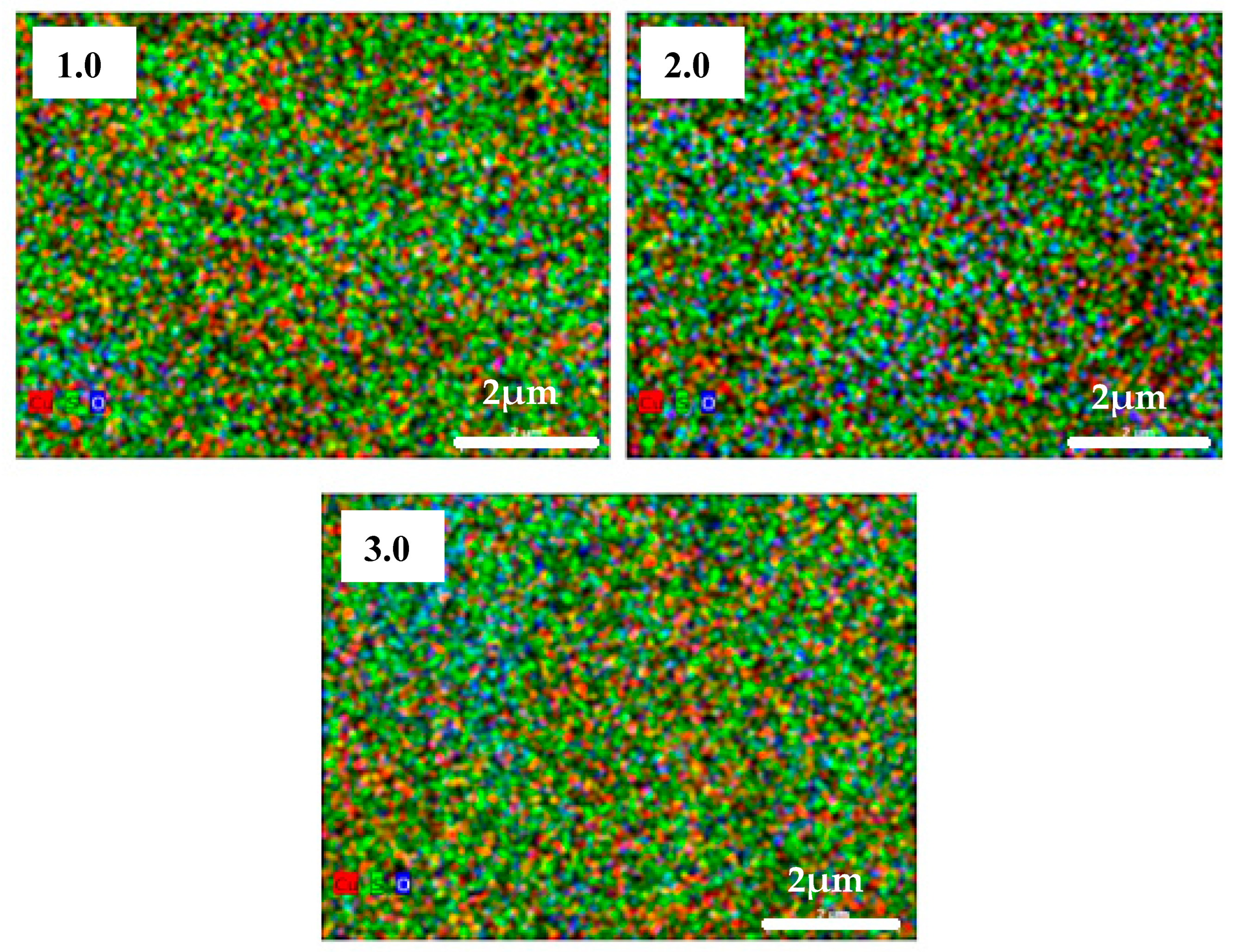
As can be seen from the data presented in Table 2, the highest percentage content in the obtained film is copper (49.4–61.0 at. %), followed by sulfur, which is slightly lower (27.9–38.0 at. %). Thus, it can be concluded that the obtained copper sulfides contain more copper atoms than sulfur. And this is confirmed by the calculated molar ratio of copper and sulfur. The molar ratio of Cu to S is significantly higher in sample 2.0, and it also has the lowest percentage of sulfur, which can be explained by the fact that in this case a lower concentration of Na2S solution (0.1 M) was used as an anionic precursor during the formation of the copper sulfide film. The different amounts of hydroquinone (samples 1.0 and 3.0) did not have a significant effect on the composition of CuxS films, as the percentages of copper and sulfur in the as-deposited films are very similar. The distribution of copper, sulfur, and oxygen can be seen on the element distribution maps of the as-deposited films in Figure 8. This picture shows how the sulfur and copper atoms are bonded to each other. Due to the unevenness of the film, oxygen from the air is adsorbed in the voids and pinholes, so it is possible to see where they are.

3.3. Optical Properties

Copper sulfides are of great interest for the production of solar cells because they can act as a light-absorbing layer in solar cells [13]. Copper sulfides are known as p-type semiconductors due to the presence of copper vacancies in the lattice. The authors of the article [21] argue that CuxS can replace the most commonly used Cu(In,Ga)Se2 in solar cells, since it has high efficiency and low cost. However, solar cells made from CuxS have only 10% efficiency and suffer from stability problems. In the study [17], it is stated that the direct band gap values of the chalcocite phases are 1.3–1.5 eV, and those of the anilite phase are 1.4 eV; therefore, it is the anilite phase, as the most stable form of copper sulfides [13], that can be used as an absorber in solar cells.
The band gap (Eg) of CuxS exhibits stoichiometry dependence. An increase in the band gap occurs with a decrease in the x value in the copper sulfides, for example, Eg is equal to 1.2 eV for Cu2S, 1.5 eV for Cu1.8S, and 2.0 eV for CuS [22]. The authors of the article [13] also state that the band gap values of copper sulfides vary with stoichiometry in CuxS and decrease with copper deficiency, as evident from band gap values in Cu2S (1.1–1.4 eV), Cu1.8S (1.5 eV), and CuS (~2.0 eV). The band gap values in the research [23] were estimated as ~1.5 eV for the Cu-rich Cu2S phase, ~1.9 eV for the Cu7.2S4 phase, and ~2.3 eV for the Cu-deficient CuS phase. This means that controlling the composition of copper sulfides is an effective way to tune their optoelectronic properties according to requirements [13].
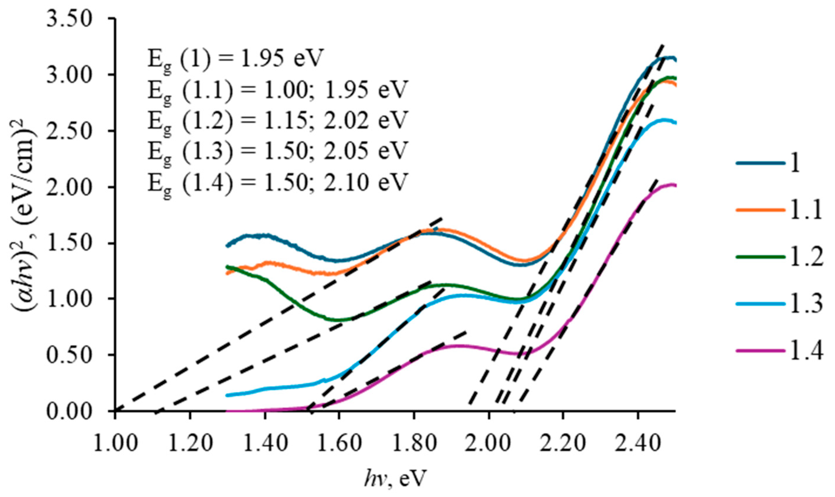
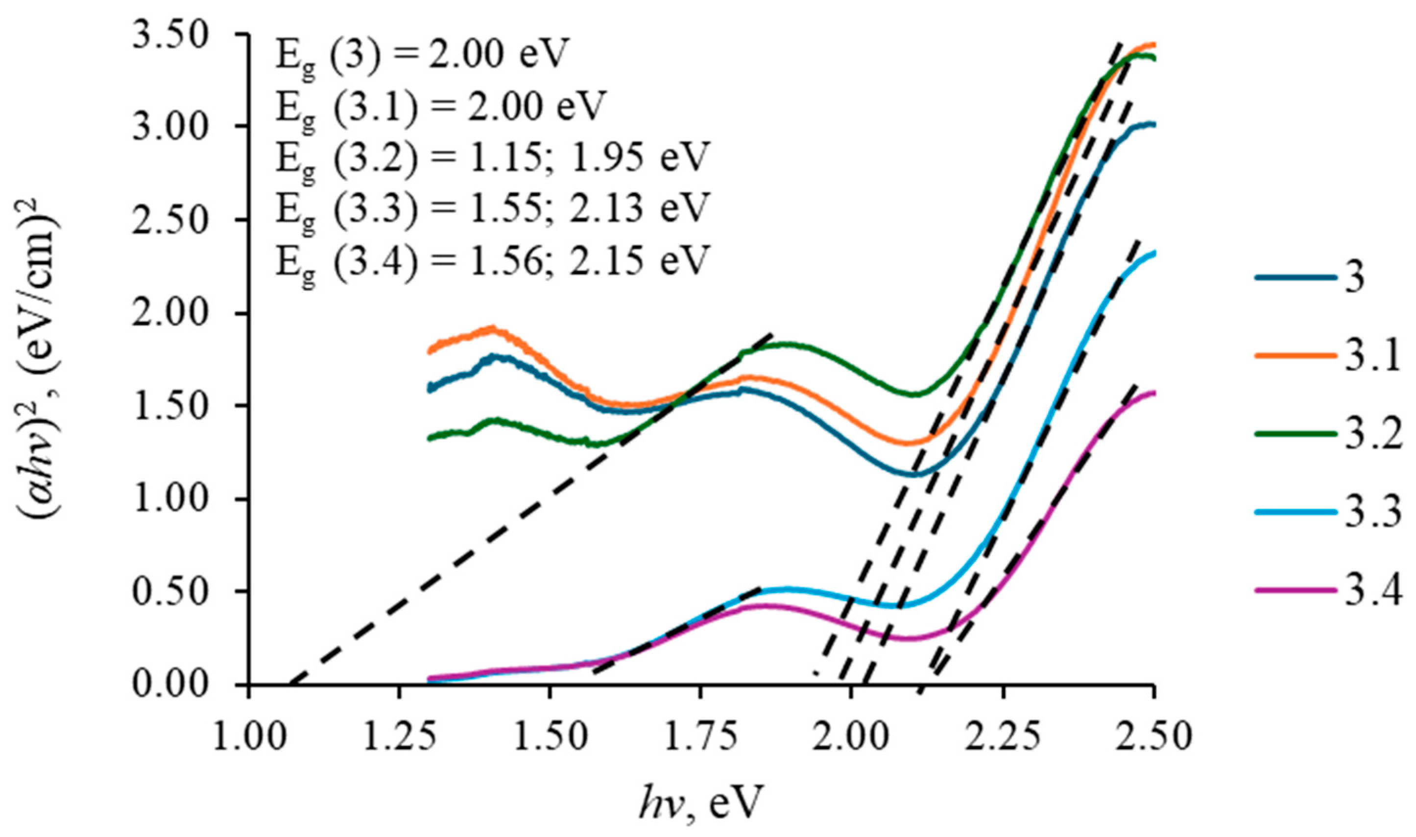
The Tauc’s plot between (αhυ)n and photon energy (hυ) was plotted to find out the optical band gap using the previously described method [24,25,26], from the absorption spectra, as seen in Figure 9, Figure 10 and Figure 11. The best linear fit was found corresponding to n = 2, which indicates direct band gap of the deposited and heated copper sulfide films. The direct band gap energies of the as-deposited and annealed CuxS films were determined by extrapolating the straight-line portion of the plot to intersect the hυ axis and were found in the range of 1.0–2.15 eV. Since there are no tin peaks in the EDS spectra, the band gap values belong to copper sulfides. Several Eg values were obtained because X-ray diffraction analysis showed that the films contain different CuxS phases. The band gap values are given in the legends and are very similar to those described theoretically.
As can be seen from the presented data (Figure 9, Figure 10 and Figure 11), almost all samples contain two band gap values corresponding to copper sulfides and depending on the value of x. Based on XRD analysis, the polycrystalline nature of the copper sulfide film with several copper sulfide phases in the samples was determined; therefore, several values of the band gap energy corresponding to CuxS with different x values were obtained. The band gap value of the as-deposited and annealed at 100 °C samples is close to 2.0 eV, which is consistent with the X-ray diffraction analysis data, since the samples are dominated by CuxS phases with a low x value.
The band gap values of the samples annealed at high temperatures (200, 300, and 400 °C) are also in the range of 1.0–1.56 eV, which corresponds to the chalcocite, djurleite, and anilite phases.

4. Conclusions

In this work, copper sulfide thin films were successfully synthesized using the sequential ionic layer adsorption and reaction (SILAR) method by varying the concentrations of cationic and anionic precursors. Structural characterization revealed that the films primarily consist of anilite, djurleite, yarrowite, and chalcocite phases, and that the phase composition can be moderately tuned through precursor concentration and annealing temperature. Notably, increasing the annealing temperature promoted a shift toward djurleite and anilite as dominant phases.
Morphological analysis using SEM showed that precursor concentration significantly affects film compactness and grain growth, with higher annealing temperatures leading to grain agglomeration. EDS confirmed copper and sulfur as the main elements, with variations in the Cu:S molar ratio (1.4 to 2.2) depending on synthesis conditions. Optical characterization indicated that the films possess band gap energies in the range of 1.0–1.5 and 1.95–2.15 eV, consistent with copper sulfide materials, though these values were relatively stable across different annealing temperatures and precursor concentrations.
The main contribution of this study lies in demonstrating how the phase composition, morphology, and optical properties of CuxS thin films can be subtly but systematically controlled through a low-cost, scalable SILAR technique, without the need for complex equipment. This provides valuable insights into the phase engineering of copper sulfides and offers a practical pathway to optimize their structural properties for applications in thin film-based sensors, optoelectronics, and photovoltaic systems. By linking synthesis parameters to phase behavior and morphology, this study addresses a previously underexplored area in copper sulfide thin film development.

Author Contributions

Conceptualization, I.A.; methodology, I.A.; software, A.B.; validation, A.B. and IA.; formal analysis, D.Z.; investigation, A.B. and D.Z.; resources, I.A.; data curation, I.A.; writing—original draft preparation, I.A. and A.B.; writing—review and editing, I.A.; visualization, D.Z.; supervision, I.A. All authors have read and agreed to the published version of the manuscript.

Funding

This research received no external funding.

Institutional Review Board Statement

Not applicable.

Informed Consent Statement

Not applicable.

Data Availability Statement

The original contributions presented in this study are included in the article. Further inquiries can be directed to the corresponding author.

Conflicts of Interest

The authors declare no conflicts of interest.

References

  1. Samdhyan, K.; Chand, P.; Anand, H. Effective Doping of Phosphorus in Copper Sulfide for High Performance Energy Storage Devices. J. Alloys Compd. 2023, 936, 168322. [Google Scholar] [CrossRef]
  2. Chiu, Y.H.; Chung, R.J.; Yougbaré, S.; Lin, L.Y. Novel Synthesis of Copper Sulfide Plate-Assembled Hollow Cages as Electrocapacitive Material of Energy Storage Device. J. Solid State Chem. 2023, 324, 124096. [Google Scholar] [CrossRef]
  3. Meng, X.; Riha, S.C.; Libera, J.A.; Wu, Q.; Wang, H.H.; Martinson, A.B.F.; Elam, J.W. Tunable Core-Shell Single-Walled Carbon Nanotube-Cu2S Networked Nanocomposites as High-Performance Cathodes for Lithium-Ion Batteries. J. Power Sources 2015, 280, 621–629. [Google Scholar] [CrossRef]
  4. Kim, W.J.; Cho, S.; Hong, J.; Hong, J.P. Hierarchically Nanostructured 1D-2D Flowerlike Copper Sulfide Electrode for High-Performance Supercapacitor Application by One-Pot Synthetic Procedure. Appl. Surf. Sci. 2022, 578, 152086. [Google Scholar] [CrossRef]
  5. Geng, P.; Zheng, S.; Tang, H.; Zhu, R.; Zhang, L.; Cao, S.; Xue, H.; Pang, H. Transition Metal Sulfides Based on Graphene for Electrochemical Energy Storage. Adv. Energy Mater. 2018, 8, 1703259. [Google Scholar] [CrossRef]
  6. Xiong, F.; Yuan, K.; Aftab, W.; Jiang, H.; Shi, J.; Liang, Z.; Gao, S.; Zhong, R.; Wang, H.; Zou, R. Copper Sulfide Nanodisk-Doped Solid-Solid Phase Change Materials for Full Spectrum Solar-Thermal Energy Harvesting and Storage. ACS Appl. Mater. Interfaces 2021, 13, 1377–1385. [Google Scholar] [CrossRef]
  7. Majumdar, D. Recent Progress in Copper Sulfide Based Nanomaterials for High Energy Supercapacitor Applications. J. Electroanal. Chem. 2021, 880, 114825. [Google Scholar] [CrossRef]
  8. Chandrasekaran, S.; Yao, L.; Deng, L.; Bowen, C.; Zhang, Y.; Chen, S.; Lin, Z.; Peng, F.; Zhang, P. Recent Advances in Metal Sulfides: From Controlled Fabrication to Electrocatalytic, Photocatalytic and Photoelectrochemical Water Splitting and Beyond. Chem. Soc. Rev. 2019, 48, 4178–4280. [Google Scholar] [CrossRef]
  9. Zhang, L.; Guo, Y.; Iqbal, A.; Li, B.; Gong, D.; Liu, W.; Iqbal, K.; Liu, W.; Qin, W. One-Step Synthesis of the 3D Flower-like Heterostructure MoS2/CuS Nanohybrid for Electrocatalytic Hydrogen Evolution. Int. J. Hydrogen Energy 2018, 43, 1251–1260. [Google Scholar] [CrossRef]
  10. Shi, Y.; Yang, B.; Guo, X.; Wu, X.; Pang, H. Copper Sulfides and Their Composites for High-Performance Rechargeable Batteries. Mater. Today Chem. 2022, 23, 100675. [Google Scholar] [CrossRef]
  11. Liu, M.; Liu, Y.; Gu, B.; Wei, X.; Xu, G.; Wang, X.; Swihart, M.T.; Yong, K.T. Recent Advances in Copper Sulphide-Based Nanoheterostructures. Chem. Soc. Rev. 2019, 48, 4950–4965. [Google Scholar] [CrossRef]
  12. Tezuka, K.; Sheets, W.C.; Kurihara, R.; Shan, Y.J.; Imoto, H.; Marks, T.J.; Poeppelmeier, K.R. Synthesis of Covellite (CuS) from the Elements. Solid State Sci. 2007, 9, 95–99. [Google Scholar] [CrossRef]
  13. Roy, P.; Srivastava, S.K. Nanostructured Copper Sulfides: Synthesis, Properties and Applications. CrystEngComm 2015, 17, 7801–7815. [Google Scholar] [CrossRef]
  14. Podder, J.; Kobayashi, R.; Ichimura, M. Photochemical Deposition of CuxS Thin Films from Aqueous Solutions. Thin. Solid. Films 2005, 472, 71–75. [Google Scholar] [CrossRef]
  15. Ratnayake, S.P.; Ren, J.; Colusso, E.; Guglielmi, M.; Martucci, A.; Della Gaspera, E. SILAR Deposition of Metal Oxide Nanostructured Films. Small 2021, 17, 2101666. [Google Scholar] [CrossRef]
  16. Rickard, D.T. Copper Sulphide Formation Chemistry at Low Temperatures; Springer: Berlin/Heidelberg, Germany, 1972. [Google Scholar]
  17. Wei, S.-H.; Xu, Q.; Huang, B.; Zhao, Y.; Yan, Y.; Noufi, R. Stability and electronic structures of CuxS solar cell absorbers. In Proceedings of the 2012 38th IEEE Photovoltaic Specialists Conference, Austin, TX, USA, 3–8 June 2012. [Google Scholar]
  18. Chen, M.; Li, K.; Luo, Y.; Shi, J.; Weng, C.; Gao, L.; Duan, G. Improved SERS Activity of Non-Stoichiometric Copper Sulfide Nanostructures Related to Charge-Transfer Resonance. Phys. Chem. Chem. Phys. 2020, 22, 5145–5153. [Google Scholar] [CrossRef] [PubMed]
  19. Dunn, J.G.; Ginting, A.R.; O’connor, B. A Thermoanalytical Study of the Oxidation of Chalcocite. J. Therm. Anal. Calorim. 1994, 41, 671–686. [Google Scholar] [CrossRef]
  20. Rawat, P.; Kala, S. Effect of Annealing on Structure and Morphology of Copper Sulfide Nanoparticles Prepared by Green Methodology. Mater. Today Proc. 2022, 67, 719–725. [Google Scholar] [CrossRef]
  21. Xu, Q.; Huang, B.; Zhao, Y.; Yan, Y.; Noufi, R.; Wei, S.H. Crystal and Electronic Structures of Cu XS Solar Cell Absorbers. Appl. Phys. Lett. 2012, 100, 3682503. [Google Scholar] [CrossRef]
  22. Zhao, Y.; Pan, H.; Lou, Y.; Qiu, X.; Zhu, J.; Burda, C. Plasmonic Cu 2-XS Nanocrystals: Optical and Structural Properties of Copper-Deficient Copper(I) Sulfides. J. Am. Chem. Soc. 2009, 131, 4253–4261. [Google Scholar] [CrossRef]
  23. Senthilkumar, M.; Mary, C.I.; Manobalaji, G.; Babu, S.M. Ligand Assisted Tunability of Morphological and Optical Properties of Copper Sulfide Nanocrystals. Mater. Sci. Semicond. Process 2019, 104, 104685. [Google Scholar] [CrossRef]
  24. Vikraman, D.; Thiagarajan, S.; Karuppasamy, K.; Sanmugam, A.; Choi, J.H.; Prasanna, K.; Maiyalagan, T.; Thaiyan, M.; Kim, H.S. Shape- and Size-Tunable Synthesis of Tin Sulfide Thin Films for Energy Applications by Electrodeposition. Appl. Surf. Sci. 2019, 479, 167–176. [Google Scholar] [CrossRef]
  25. Bronusiene, A.; Popov, A.; Barauskiene, I.; Ancutiene, I. Effect of Ascorbic Acid on the Properties of Tin Sulfide Films for Supercapacitor Application. Surf. Interfaces 2021, 25, 101275. [Google Scholar] [CrossRef]
  26. Bronusiene, A.; Kleinauskas, R.; Ancutiene, I. Facile Synthesis and Characterization of TiO2/SnS Nanocomposites by Eco-Friendly Methods. Coatings 2024, 14, 88. [Google Scholar] [CrossRef]
Figure 1. Schematic representation of experimental steps for obtaining CuxS films on FTO glass sheets using the SILAR method.
Coatings 15 01221 g001
Figure 2. Crystal structures of some copper sulfides.
Coatings 15 01221 g002
Figure 3. X-ray diffraction patterns of CuxS films prepared using 0.2 M CuSO4 solution with 0.2 M hydroquinone and 0.2 M Na2S, as-deposited (1.0) and annealed at 100 °C (1.1), 200 °C (1.2), 300 °C (1.3), and 400 °C (1.4). Abbreviations: Ch—chalcocite, Dj—Djurleite, A—Anilite, Y—Yarrowite.
Coatings 15 01221 g003
Figure 4. X-ray diffraction patterns of CuxS films prepared using 0.2 M CuSO4 solution with 0.2 M hydroquinone and 0.1 M Na2S, as-deposited (2.0) and annealed at 100 °C (2.1), 200 °C (2.2), 300 °C (2.3), and 400 °C (2.4). Abbreviations: Ch—chalcocite, Dj—Djurleite, A—Anilite, Y—Yarrowite.
Coatings 15 01221 g004
Figure 5. X-ray diffraction patterns of CuxS films prepared using 0.2 M CuSO4 solution with 0.1 M hydroquinone and 0.2 M Na2S, as-deposited (3.0) and annealed at 100 °C (3.1), 200 °C (3.2), 300 °C (3.3), and 400 °C (3.4). Abbreviations: Ch—chalcocite, Dj—Djurleite, A—Anilite, Y—Yarrowite.
Coatings 15 01221 g005
Figure 6. SEM images of as-deposited CuxS film surface; magnification of 10,000×. Precursors: 1.0—0.2 M CuSO4 solution with 0.2 M hydroquinone and 0.2 M Na2S solution; 2.0—0.2 M CuSO4 solution with 0.2 M hydroquinone and 0.1 M Na2S solution; 3.0—0.2 M CuSO4 solution with 0.1 M hydroquinone and 0.2 M Na2S solution.
Coatings 15 01221 g006
Figure 7. SEM images of annealed CuxS film surface; magnification of 10,000×. The films were prepared using 0.2 M CuSO4, 0.2 M hydroquinone, and 0.2 M Na2S solutions and annealed at different temperatures.
Coatings 15 01221 g007
Figure 8. Maps of elements in the as-deposited CuxS film: red = Cu, green = S, and blue = O.
Coatings 15 01221 g008
Figure 9. Band gap energies of CuxS films prepared using 0.2 M CuSO4 solution with 0.2 M hydroquinone and 0.2 M Na2S, as-deposited (1.0) and annealed at 100 °C (1.1), 200 °C (1.2), 300 °C (1.3), and 400 °C (1.4).
Coatings 15 01221 g009
Figure 10. Band gap energies of CuxS films prepared using 0.2 M CuSO4 solution with 0.2 M hydroquinone and 0.1 M Na2S, as-deposited (2.0) and annealed at 100 °C (2.1), 200 °C (2.2), 300 °C (2.3), and 400 °C (2.4).
Coatings 15 01221 g010
Figure 11. Band gap energies of CuxS films prepared using 0.2 M CuSO4 solution with 0.1 M hydroquinone and 0.2 M Na2S, as-deposited (3.0) and annealed at 100 °C (3.1), 200 °C (3.2), 300 °C (3.3), and 400 °C (3.4).
Coatings 15 01221 g011
Table 1. Numbering of samples.
Cationic and Anionic PrecursorsSample No
Annealing Temperature, °C
Unannealed100 °C200 °C300 °C400 °C
0.2 M CuSO4 solution with 0.2 M hydroquinone and 0.2 M Na2S solution1.01.11.21.31.4
0.2 M CuSO4 solution with 0.2 M hydroquinone and 0.1 M Na2S solution2.02.12.22.32.4
0.2 M CuSO4 solution with 0.1 M hydroquinone and 0.2 M Na2S solution3.03.13.23.33.4
Table 2. The elemental composition by EDS analysis (excluding C).
Sample No.Cu (at. %)S (at. %)O (at. %)Na (at. %)x in CuxS
1.053.6 ± 2.738.0 ± 1.07.7 ± 0.6-1.4
2.061.0 ± 3.027.9 ± 0.89.6 ± 0.7-2.2
3.049.4 ± 2.732.8 ± 1.010.3 ± 0.86.3 ± 0.81.5
Disclaimer/Publisher’s Note: The statements, opinions and data contained in all publications are solely those of the individual author(s) and contributor(s) and not of MDPI and/or the editor(s). MDPI and/or the editor(s) disclaim responsibility for any injury to people or property resulting from any ideas, methods, instructions or products referred to in the content.