
Effect of SiO2 Layer Thickness on SiO2/Si3N4 Multilayered Thin Films

Abstract
1. Introduction
2. Experimental Methods
2.1. Preparation of SiO2/Si3N4 Thin Films
2.2. Characterization of Thin-Film Structure and Properties
3. Results and Discussion
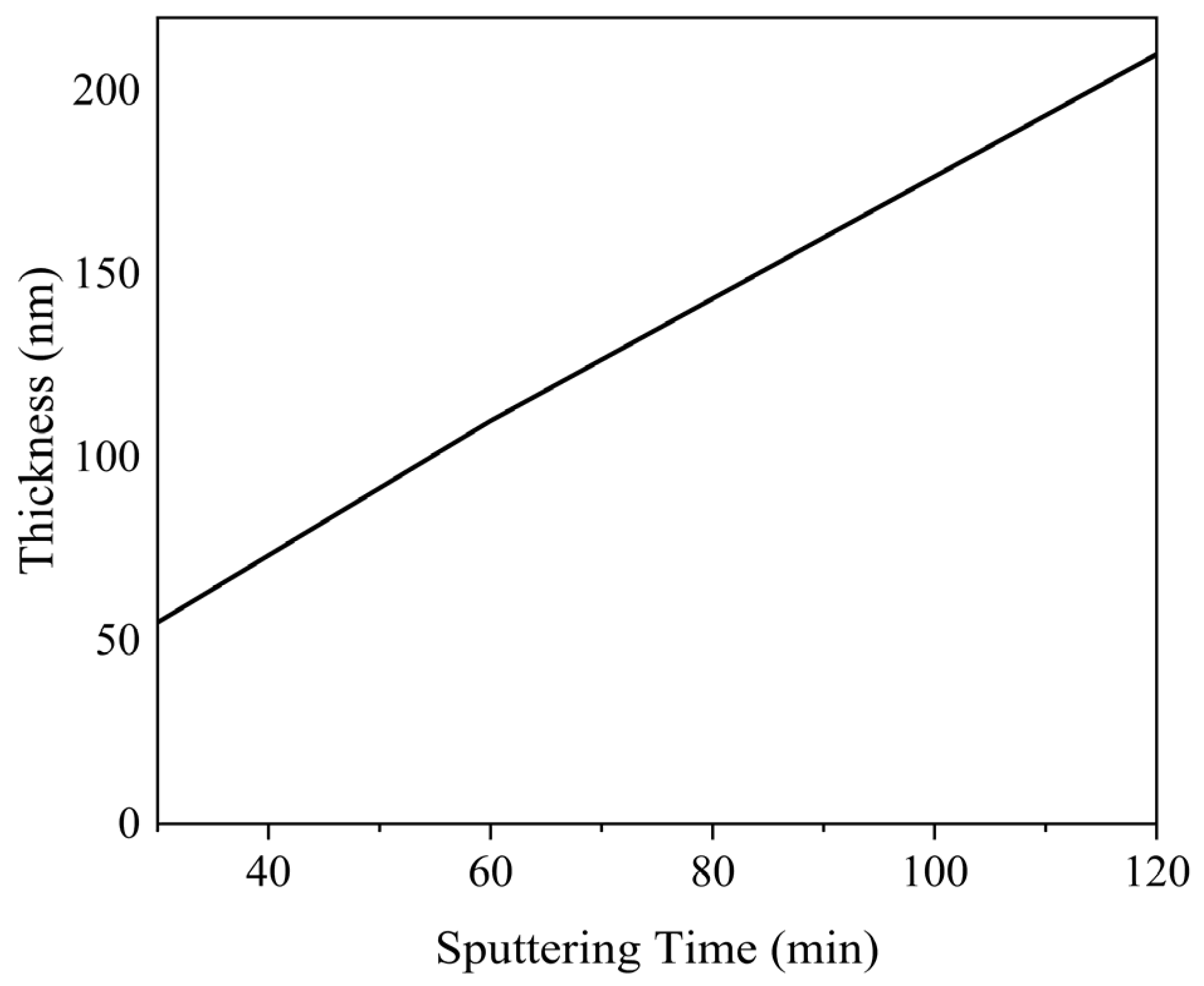
3.1. Sputtering Rate Testing of SiO2 Thin Films
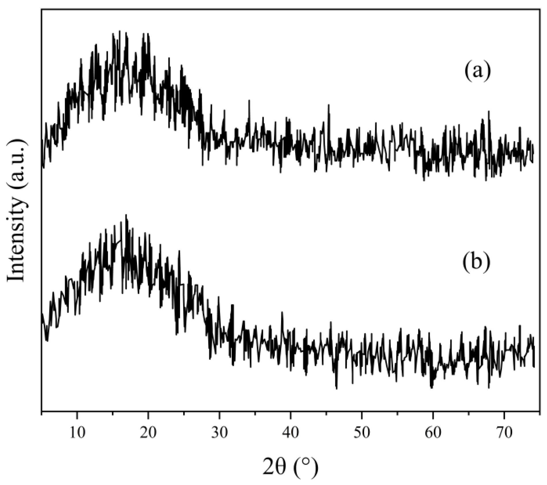
3.2. X-ray Diffraction (XRD)
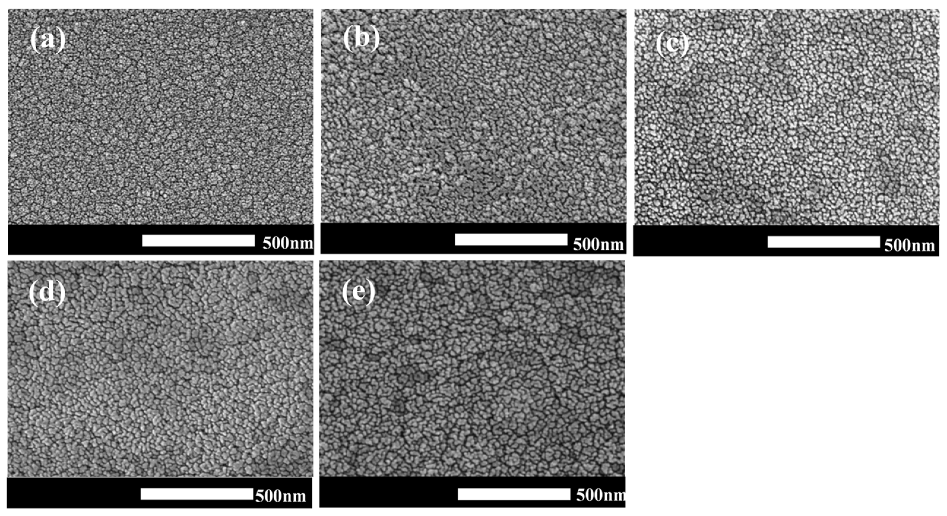
3.3. Scanning Electron Microscopy (SEM)
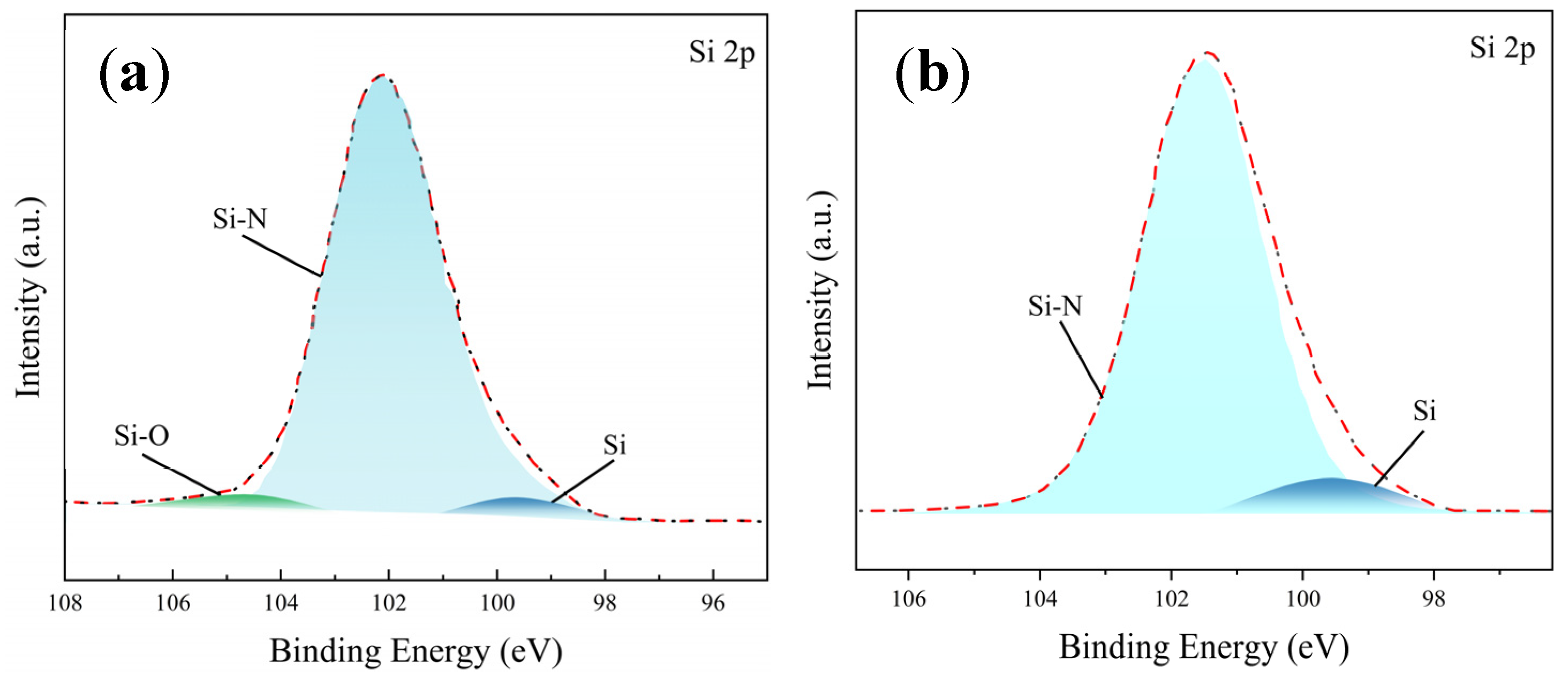
3.4. X-ray Photoelectron Spectroscopy (XPS)
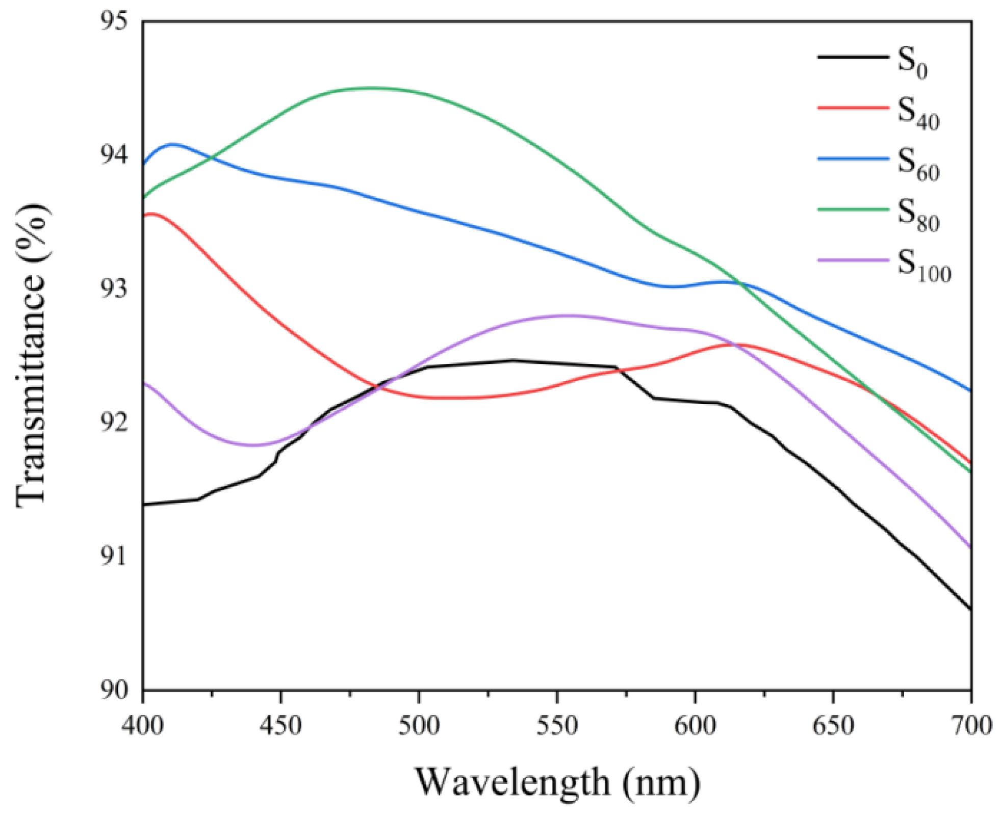
3.5. Optical Performance Analysis
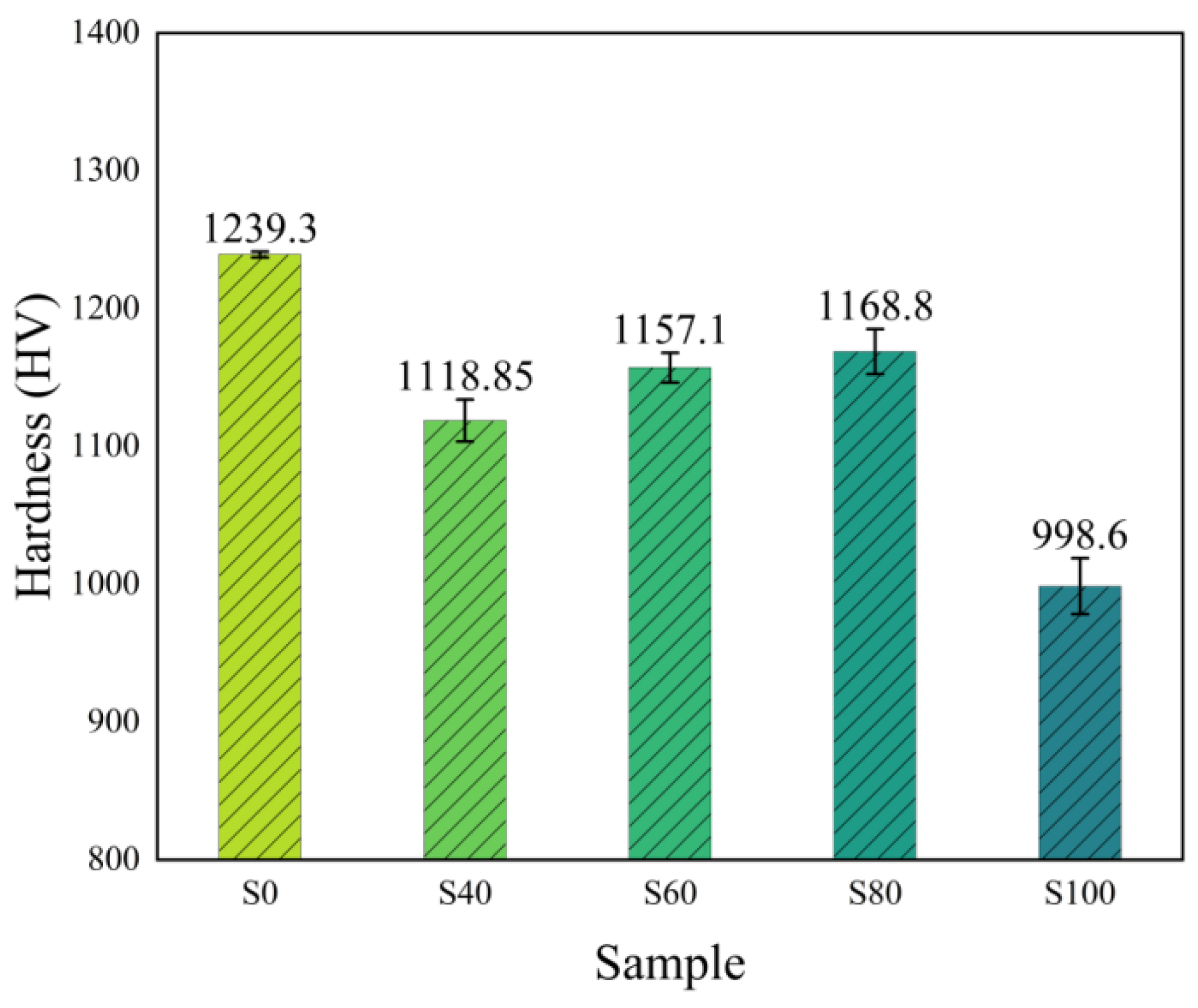
3.6. Vickers Hardness Analysis
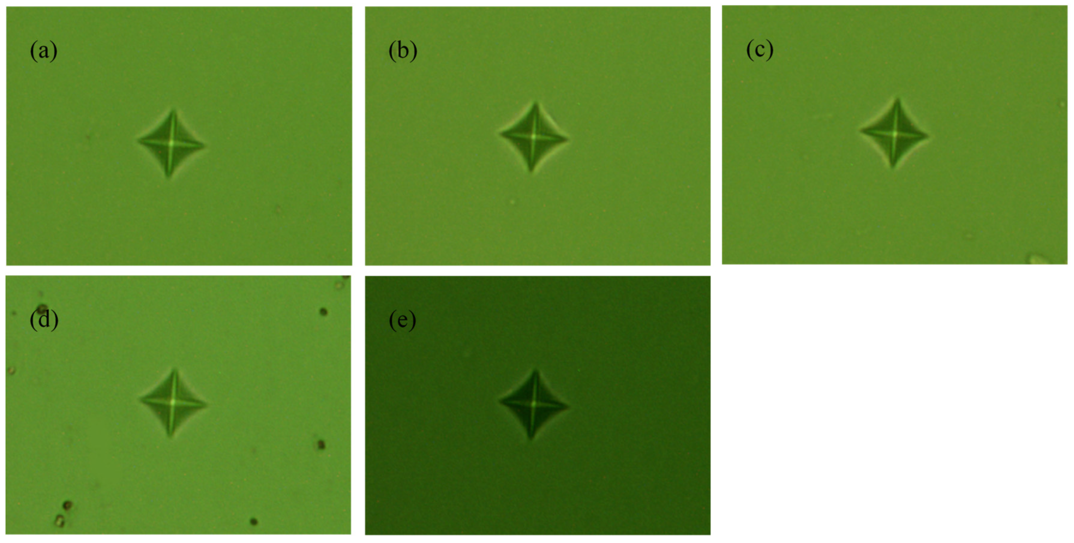
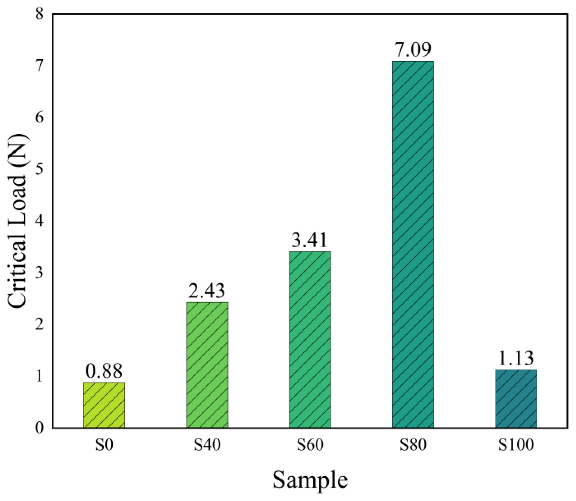
3.7. Analysis of Nanoscratch Performance
4. Conclusions
Author Contributions
Funding
Institutional Review Board Statement
Informed Consent Statement
Data Availability Statement
Conflicts of Interest
References
- Nikolett, H.; Katalin, B.; Csaba, B. Silicon Nitride and Hydrogenated Silicon Nitride Thin Films: A Review of Fabrication Methods and Applications. Materials 2021, 14, 5658. [Google Scholar] [CrossRef] [PubMed]
- Kaloyeros, A.E.; Pan, Y.; Goff, J.; Arkles, B. Review—Silicon Nitride and Silicon Nitride-Rich Thin Film Technologies: State-of-the-Art Processing Technologies, Properties, and Applications. ECS J. Solid State Sci. Technol. 2020, 9, 063006. [Google Scholar] [CrossRef]
- Kopfer, J.M.; Keipert-Colberg, S.; Borchert, D. Capacitance–voltage characterization of silicon oxide and silicon nitride coatings as passivation layers for crystalline silicon solar cells and investigation of their stability against x-radiation. Thin Solid Film. 2011, 519, 6525–6529. [Google Scholar] [CrossRef]
- Silva, J.A.; Quoizola, S.; Hernandez, E.; Thomas, L.; Massines, F. Silicon carbon nitride films as passivation and antireflective coatings for silicon solar cells. Surf. Coat. Technol. 2014, 242, 157–163. [Google Scholar] [CrossRef]
- Pariksha, M.; Harsh, G.; Santanu, G.; Pankaj, S. Study of Optical Properties of Single and Double Layered Amorphous Silicon Nitride Films for Photovoltaics Applications. Silicon 2022, 15, 143–151. [Google Scholar]
- Okada, H.; Kawakami, K.; Shinohara, M.; Ishimaru, T.; Sekiguchi, H.; Wakahara, A.; Furukawa, M. Chemical vapor deposition of silicon nitride film enhanced by surface-wave plasma for surface passivation of AlGaN/GaN device. Am. Inst. Phys. Conf. Ser. 2015, 1649, 41–46. [Google Scholar]
- Wu, E.Y.; Stathis, J.H.; Han, L.K. Ultra-thin oxide reliability for ULSI applications. Semicond. Sci. Technol. 2000, 15, 425–435. [Google Scholar] [CrossRef]
- Tao, M.; Botchkarev, A.E.; Park, D.; Reed, J.; Morkoc, H. Improved Si3N4/Si/GaAs metal nsulator: Emiconductor interfaces by in situ anneal of the as eposited Si. J. Appl. Phys. 1995, 77, 4113–4115. [Google Scholar] [CrossRef]
- Suh, D.; Kang, J. Stress-induced failure of Si3N4 metal-insulator-metal capacitors fabricated by plasma enhanced chemical vapor deposition. J. Vac. Sci. Technol. B 2002, 20, 717–720. [Google Scholar] [CrossRef]
- Wang, C.; Kim, N.Y. Fabrication of Metal-insulator-metal Capacitors with SiNx Thin Films Deposited by Plasma-enhanced Chemical Vapor Deposition. Trans. Electr. Electron. Mater. 2009, 10, 147–151. [Google Scholar] [CrossRef]
- Cong, W.; Fang, Z.; Nam-Young, K. Development and Characterization of Metal-Insulator-Metal Capacitors with SiNx Thin Films by Plasma-Enhanced Chemical Vapor Deposition. Chin. Phys. Lett. 2010, 27, 078101. [Google Scholar] [CrossRef]
- Di, Z.; Lei, H.; Juntang, Y.; Chao, L. Influences of different sputtering current on the microstructure and electrical properties of silicon nitride thin films deposited on cemented carbide tools. Ceram. Int. 2021, 47, 32160–32167. [Google Scholar]
- Khemasiri, N.; Paleeya, N.; Phromyothin, S.T.; Horprathum, M.; Sungthong, A.; Nukeaw, J.; Pratontep, S. Silicon Nitride Thin Films Deposited by Reactive Gas-timing Magnetron Sputtering for Protective Coating Applications. Adv. Mater. Lett. 2015, 6, 554–559. [Google Scholar] [CrossRef]
- Zhang, Y.T.; Wu, W.G.; Han, Y.W.; Wu, X.Y.; Cheng, Y.P.; Liu, L.J. Adhesion analysis of silicon nitride film deposited on stainless steel surface by adding transition layer. Nanotechnology 2020, 31, 215711–215720. [Google Scholar] [CrossRef] [PubMed]
- Ye, M.; Peng, Y.; Yi, Y.S. Silicon-rich silicon nitride thin films for subwavelength grating metalens. Opt. Mater. Express 2019, 9, 1200–1207. [Google Scholar] [CrossRef]
- Sheetz, B.S.; Bandara, Y.N.D.; Rickson, B.; Auten, M.; Dwyer, J.R. Rapid, General-Purpose Patterning of Silicon Nitride Thin Films Under Ambient Conditions for Applications Including Fluid Channel and SERS Substrate Formation. ACS Appl. Nano Mater. 2020, 3, 2969–2977. [Google Scholar] [CrossRef]
- You, D.; Liu, W.; Jiang, Y.; Cao, Y.; Guo, W.; Tan, M. Effect of ion assistance on silicon nitride films deposited by reactive magnetron sputtering. Mater. Sci. Semicond. Process. 2023, 157, 107312. [Google Scholar] [CrossRef]
- Li, D.; Li, B.; Tang, B.; Xiong, W.; Zhang, P.; Yang, Y.; Liu, R.; Li, Z. CMOS-compatible low stress silicon nitride films for photonic integration. In Nanophotonics and Micro/Nano Optics VI; SPIE: Bellingham, WA, USA, 2020; Volume 11556. [Google Scholar]
- Kuo, T.W.; Wang, N.F.; Tsai, Y.Z.; Hung, P.K.; Houng, M.P. Broadband triple-layer SiOx/SiOxNy/SiNx antireflective coatings in textured crystalline silicon solar cells. Mater. Sci. Semicond. Process. 2014, 25, 211–218. [Google Scholar] [CrossRef]
- Li, J.D.; Shen, G.S.; Chen, W.L.; Li, Z.; Hong, R.J. Preparation of SiNx multilayer films by mid-frequency magnetron sputtering for crystalline silicon solar cells. Mater. Sci. Semicond. Process. 2017, 59, 40–44. [Google Scholar] [CrossRef]
- Kluska, S.; Hejduk, K.; Drabczyk, K.; Lipinski, M. Optical properties and passivation effects of silicon nitride three layer stacks deposited by plasma enhanced chemical vapor deposition. Phys. Status Solidi A Appl. Mater. Sci. 2016, 213, 1839–1847. [Google Scholar] [CrossRef]
- Choi, K.; Kim, K.J. Antireflection coating of a SiO/SiN double layer on silicon fabricated by magnetron sputtering. J. Ceram. Process. Res. 2010, 11, 341–343. [Google Scholar]
- Bonilla, R.S.; Reichel, C.; Hermle, M.; Wilshaw, P.R. On the location and stability of charge in SiO2/SiNx dielectric double layers used for silicon surface passivation. J. Appl. Phys. 2014, 115, 551–1072. [Google Scholar] [CrossRef]
- Yang, X.; Wu, M.; Jian, M.; Zhu, S.; Jiang, J.; Yang, L. Feasibility of molecular dynamics simulation for process parameter guidance of silicon nitride thin films by PECVD. Appl. Surf. Sci. 2024, 654, 159401–159407. [Google Scholar] [CrossRef]
- Rodríguez-López, R.; Abundiz-Cisneros, N.; Sanginés, R.; Águila-Muñoz, J.; Machorro-Mejía, R. Plasma emission spectroscopy and optical properties of reactive-sputtered silicon oxynitride films. J. Phys. D Appl. Phys. 2024, 57, 285302. [Google Scholar] [CrossRef]


| No. | SiO2 | Si3N4 | Pressure (Pa) | Flow (sccm) | Temperature (°C) | ||
|---|---|---|---|---|---|---|---|
| Power (W) | Time (min) | Power (W) | Time (min) | ||||
| S0 | / | / | 150 | 30 | 1 | 45 | 200 |
| S40 | 150 | 40 | 150 | 30 | 1 | 45 | 200 |
| S60 | 150 | 60 | 150 | 30 | 1 | 45 | 200 |
| S80 | 150 | 80 | 150 | 30 | 1 | 45 | 200 |
| S100 | 150 | 100 | 150 | 30 | 1 | 45 | 200 |
Disclaimer/Publisher’s Note: The statements, opinions and data contained in all publications are solely those of the individual author(s) and contributor(s) and not of MDPI and/or the editor(s). MDPI and/or the editor(s) disclaim responsibility for any injury to people or property resulting from any ideas, methods, instructions or products referred to in the content. |
© 2024 by the authors. Licensee MDPI, Basel, Switzerland. This article is an open access article distributed under the terms and conditions of the Creative Commons Attribution (CC BY) license (https://creativecommons.org/licenses/by/4.0/).
Share and Cite
Huang, Z.; Duan, J.; Li, M.; Ma, Y.; Jiang, H. Effect of SiO2 Layer Thickness on SiO2/Si3N4 Multilayered Thin Films. Coatings 2024, 14, 881. https://doi.org/10.3390/coatings14070881
Huang Z, Duan J, Li M, Ma Y, Jiang H. Effect of SiO2 Layer Thickness on SiO2/Si3N4 Multilayered Thin Films. Coatings. 2024; 14(7):881. https://doi.org/10.3390/coatings14070881
Chicago/Turabian StyleHuang, Ziming, Jiaqi Duan, Minghan Li, Yanping Ma, and Hong Jiang. 2024. "Effect of SiO2 Layer Thickness on SiO2/Si3N4 Multilayered Thin Films" Coatings 14, no. 7: 881. https://doi.org/10.3390/coatings14070881
APA StyleHuang, Z., Duan, J., Li, M., Ma, Y., & Jiang, H. (2024). Effect of SiO2 Layer Thickness on SiO2/Si3N4 Multilayered Thin Films. Coatings, 14(7), 881. https://doi.org/10.3390/coatings14070881