1. Introduction
In many industrial processes (such as the metallurgical industry, the recycling of various wastes, etc.), during the production of various products, large amounts of heat are released as a byproduct [
1]. A large part of the heat is lost as energy. It is stated in the literature that even one third of the heat intended for heating cities is lost in transmission lines [
1,
2]. As industrial processes develop, more and more heat losses are generated, and the problem arises as to how to use this heat efficiently to extract other types of energy, such as, e.g., electricity. One of the ways to convert the generated heat into electricity is the use of a thermoelectric generator (TEG) [
1,
2]. These devices can be used not only to convert excess heat into electricity, but also as renewable energy sources [
3,
4,
5,
6]. TEGs are used in a variety of applications for electricity generation, including powering space probes such as the Mars Curiosity rover. In addition, TEGs contribute to increasing the efficiency of hybrid cars by converting some of the heat generated by internal combustion engines into electricity. TEGs can be used to create hybrid solar cells that use both visible light and the infrared wavelength range waves. Experimental devices have been developed that are adapted for electricity generation by taking advantage of the fact that there is a temperature difference between the surface and deep layers of natural water bodies [
1,
7,
8,
9,
10].
If one side of the (TEG) piece of metal is heated at a certain time, while the other side is cooled, the electrons on the hot side will have more energy than the equivalent electrons on the cooler side, meaning that the hot electrons have more kinetic energy than those on the cooler side. So, the hot electrons travel to the cold side faster than the cold electrons move towards the hot side, and, finally, the cold end of the thermoelectric generator is negatively charged, and the hot end is charged positively. Due to this voltage, a potential difference is obtained. The operation of these devices is based on the principle of the Seebeck effect [
1,
2,
3]. The efficiency of TEG devices is low and reaches up to 10%, but these are relatively simple devices that serve for a long time and do not require frequent maintenance [
1]. In addition, these devices operate without noise, while producing electricity, and do not emit any harmful substances into the environment. TEG devices can also be made from semiconductor materials, such as silicon, gallium arsenide, or others [
1,
2,
3,
4]. However, making TEGs from semiconductors is more expensive than making them from metals because semiconductors require doping to make them P- or N-type semiconductors. The main task for researchers when forming TEGs is to obtain materials with the highest electrical conductivity, but the lowest thermal conductivity [
2,
11,
12,
13,
14]. These two factors determine the efficiency of TEG while producing electricity from heat. In order to improve the efficiency of TEGs, scientists use various combinations of materials and nanoparticles for their formation, in such a way that the heat flow is slowed down without hindering the free flow of electrical particles. Materials such as bismuth telluride (Bi
2Te
3), lead telluride (PbTe) and others are often used in TEG production [
2,
3]. One of the main parameters defining the suitability of a material for TEG production is the Seebeck coefficient, whose expression is as follows: S = ∆V/∆T, where ∆V is the potential difference between different heated and cooled metal ends, and ∆T is the temperature difference between these different metals [
1,
2,
15,
16,
17,
18]. Another important factor that must be taken into account when manufacturing TEGs is thermal expansion and plasticity, since at different temperatures, materials expand unequally, and various micro-strains and lattice defects are formed [
1,
2,
3,
4]. In the case of insufficient plasticity and temperature changes, the produced TEG may lose its operational properties faster [
2,
19,
20,
21,
22]. The compatibility coefficient (denoted by the letter S) is used to determine the compatibility of materials in the production of TEG. The literature states that if the compatibility coefficient between the materials differs by more than two times, the TEG device is unsuitable for use, as it will work inefficiently [
1,
2]. The materials used for the production of TEGs are divided into low temperature (TEG operation up to 450 K, with materials such as bismuth (Bi), which is combined with antimony (Sb), tellurium (Te), etc.), medium temperature (operating up to 850 K; various lead alloys are used). High-temperature materials—up to 1300 K—are semiconductors such as silicon–germanium (SiGe) alloys, etc. [
1,
2,
3,
22,
23,
24,
25,
26].
Additional materials are often used to improve the efficiency of TEGs, allowing them to store the generated excess heat. One of such materials is a phase change material (PCM) [
1,
2]. PCM stores thermal energy by changing phase and can release it (as thermal energy) when needed, e.g., for the heating of a TEG active element. In this way, when creating PCM and TEG hybrid systems, it is possible to improve the efficiency of the process when the generated excess heat is used to generate electricity [
2]. The modern production design of TEG devices is constantly improving, and more and more complex structures are produced. TEGs must have both good performance characteristics and wide versatility, which depends on very specific heat-releasing systems [
2,
27,
28,
29,
30]. Various methods, such as plasma thermal deposition, material diffusion technology, etc. are used to manufacture TEGs and expand the design functionality. In order to improve the thermal characteristics of TEGs, active elements of TEG are coated with heat insulators, such as metal ceramics, etc. [
1,
2,
3]. In order to use TEGs for electricity generation, it is necessary to form a very thin (20–300 nm) active layer with superior plasticity and flexibility from various irregularly shaped surfaces. In this case, it is necessary that the geometric shape of the TEG surface reproduces the irregular relief of the heating surface. A thin layer has a lower thermal conductivity, which allows more efficient use of the temperature difference between the warm and cold surface, which is necessary for the Seebeck effect to work. Thin layers can have a higher Seebeck coefficient. This is important, because a higher Seebeck coefficient means a higher generated electrical voltage at the same temperature difference. Thin layers (can be flexible, not only thin) adapt more easily to irregular surfaces and shapes. This is important, if you want to integrate TEG into various forms, such as bendable objects, or even clothing. In addition, the use of thin nano-metric layers for TEG allows to ensure that the mass and dimensions of the overall system will not be increased [
2,
3,
31,
32,
33,
34].
The Bi-Ni combination was chosen in this research because both bismuth and nickel have low thermal conductivity, which helps to ensure high working efficiency for electricity generation. In addition, such combination can work at relatively high temperatures (e.g., in a waste incineration reactor, where the process temperature is up to 1200 K, etc.) because the melting temperature of Ni is 1726 K. The Bi-Ni combination is long-lasting and stable because no chemical reaction occurs between the materials and an environment that may contain various compounds (e.g., in a household waste processing reactor). When forming thin TEG layers (e.g., using the magnetron sputtering method, etc.), it is recommended that the junction is made of single-component metals, since using their alloy or composite (compound) greatly increases the probability of mechanical defects. Meanwhile, when using single-component materials (as in the case of this study, with the Bi-Ni junction), it is technologically possible to obtain solid layers, which are characterized by good plasticity and thermal expansion compatibility. Using compounds (composites), poses a huge problem when working with TEG (thin-layers 20–300 nm) in a high-temperature environment (800 K and more) due to the stability of the layer structure (stresses, defects are formed, plasticity decreases, etc.).
In order to fill the gaps in the thin-film TEG results in the scientific literature, the purpose of this work is to form a thin-film Bi-Ni (TEG) using magnetron sputtering deposition technology and to study its characteristics.
2. Materials and Methods
Magnetron sputtering technology was used to form the thin-film TEG. The TEG layer is formed from bismuth (Bi) and nickel layers (Ni).
Bilayer structures composed of bismuth and nickel were grown utilizing DC magnetron sputtering within an argon gas environment, maintaining a pressure (p) of 1.33 Pa to ensure deposition process stability. To regulate the gas environment, an argon flow meter connected to the chamber enabled the adjustment of oxygen gas flow rates within the range of 0 to 500 cm
3/min. The bismuth and nickel disc targets, each possessing a 3-inch diameter, were sourced from Kurt J. Lesker Company in Jefferson Hills, PA, USA, with a noteworthy purity of 99.95%. The spatial arrangement of the deposition system involved maintaining a constant distance of 6 cm between the magnetrons and the substrate, as illustrated in
Figure 1a. Notably, the fixed target currents for bismuth and nickel were set at 0.2 A and 0.5 A, respectively. During the magnetron deposition process, the samples were subjected to a controlled heating mechanism, maintaining a substrate temperature of 423 K. Elevating the substrate temperature serves a dual purpose: enhancing adhesion between the deposited layers and the substrate, and augmenting the energy and mobility of atoms on the substrate surface. This strategic manipulation of temperature contributes to the overall quality and characteristics of the deposited bilayer structures. The deposition times for bismuth and nickel were precisely delineated at 5 min and 10 min, respectively. This temporal control plays a pivotal role in determining the thickness and properties of the resultant layers, ensuring a tailored approach to achieving the desired bilayer structure. In summary, this detailed deposition process involves a comprehensive control strategy, encompassing gas flow rates, pressure, target currents, substrate temperature, and deposition times. The thickness of each layer was about 50–100 nm.
The bismuth layer was grown first because half of the wafer was covered with a silicon wafer. The silicon wafer was then placed on top of the previously deposited Bi layer, and a nickel layer was grown. In order to form the Bi-Ni junction, during the formation of the nickel layer, part of the Bi layer (5 mm) was exposed (not covered by the silicon wafer; for this reason, a portion of the nickel layer covered the surface of the open bismuth part, thus forming the Bi-Ni junction). The width of the Bi layer is 5 mm, the length is 25 mm, and the width of the Ni layer is 5 mm and the length is 30 mm. The total surface area of the TEG (including Bi and Ni layers) is 275 mm
2. A general schematic view (concept) of the TEG is presented in
Figure 1b. The substrate is a thin 0.1 mm steel sheet coated with a non-conductive dielectric Al
2O
3 surface. Spiral-shaped nichrome wire (diameter—0.5 mm and length—150 mm) is used for TEG heating. The Ni layer was heated because it is considered to be resistant to high temperatures.
The temperature difference in the TEG junction was measured using copper-constantan thermocouples. Two thermocouples were used to measure the temperature difference: one thermocouple measured the temperature of the Bi layer, while the other thermocouple measured the temperature of the Ni layer. In order to maintain the temperature difference between the Bi and Ni layers, the Bi layer was immersed in melting ice (about 50% of the Bi surface area was immersed, while maintaining a distance of about 12.5 mm between the Bi-Ni junction and the ice-immersed part). Meanwhile, the Ni layer, 50% of the surface area, was heated using a nichrome wire, keeping a distance of about 15 mm between the Bi-Ni junction and the heated Ni part.
The heat flux of TEG was found using the formula: Q = S·ΔT, where S is the thermoelectric power (which is found based on the Seebeck coefficient values); and ΔT is the temperature difference between the hot and cold sides of the TEG.
A Hitachi S-3400 N model scanning electron microscope (SEM) was used to evaluate the surface morphology of the Bi-Ni layer. Meanwhile, the energy dispersive X-ray spectroscopy (EDS) method was used to determine the elemental composition of the surface, which was performed together with surface scanning electron microscopy. X-ray diffraction (XRD) with standard Bragg–Brentan focusing was used for the crystallographic study of the samples. When determining the operating characteristics of the formed TEG, heating was carried out using a heater made of nichrome wire. Electrical characteristics (including results for copper-constantan thermocouples) were measured using a Keithley 5487 multimeter, transmitting data to a computer.
3. Results and Discussion
TEG was formed from the junction of the dissimilar metals bismuth (Bi) and nickel (Ni). Bismuth is the most suitable metal for TEG formation, as it has the highest efficiency in converting heat energy into electricity [
1]. Meanwhile, nickel was chosen because it has good resistance to environmental conditions, as well as good mechanical flexibility and electrical conductivity. During this research work, the goal was to form a thin-layer (about 100–300 nm thick) TEG element. The method of magnetron sputtering was chosen for the formation of TEG because using this technology makes it possible to control the thickness of the grown layer precisely, and the resulting Bi-Ni layer is dense, non-porous.
Figure 2 shows the surface microrelief image of the Bi-Ni layer obtained by SEM.
Figure 1a shows the surface of the Bi-Ni layer at 200× microscope magnification. The layer has a visible Bi-Ni junction (the boundary between the dark and light layers). Therefore, we can say that the Bi-Ni layer has a good electrical contact.
Figure 1b shows the surface of the TEG at a SEM magnification of 500. A clear boundary between the layers is also visible in this figure.
Figure 2c,d are SEM images when the magnification is 1000 and 2000, respectively. It can be noticed that in this case, the boundary of the Bi-Ni layer is not so clearly visible. In addition, it is possible to observe formed formations of irregular shape on the surface, the dimensions of which change within the limits of 1–3 µm. These irregularly shaped formations are formed during magnetron sputtering. Some of the microstructures on the surface are similar to the shape of a drop. This is because, as the layers grow, the material undergoes phase transformations (crystallization, when the material changes from a liquid state to a solid state). In addition, derivatives (on the TEG surface) are formed in such a way that the surface bond energy is the lowest.
Figure 3 shows the elemental distribution of the TEG (Bi-Ni) layer on the surface using the EDS method.
Figure 3a shows an image of the surface of the TEG (magnification of 1000) obtained using SEM, which measured the distribution of the elemental composition on the surface.
Figure 2b shows the surface distribution of bismuth, nickel, and oxygen. As it can be seen, the red color represents the distribution of nickel, the green color bismuth, and the blue color the oxygen on the surface. A clear Bi-Ni junction boundary is also visible in this figure.
Figure 3c shows the surface distribution of bismuth (green), while
Figure 3d shows the surface distribution of nickel. According to the color distribution of the elements, both Bi and Ni layers can be identified in the SEM images. In this case, in the previous SEM images, the brighter area represents the Bi layer, while the darker one the Ni layer.
In addition, it can be stated that the formed Bi-Ni layers are technologically suitable, since there is a clearly visible color border marking the deviation of their elemental composition. The percentage elemental composition of the surface was determined using the EDS method. EDS studies facilitate the determination of the elemental composition of the TEG surface (which is especially useful in the production of TEG from various components) and the distribution of individual elements over the entire area. In addition, it allows to identify whether the TEG is composed of the right (planned) elements. EDS studies complement other methods (e.g., XRD, as in the case of this study), as it is possible to identify the composition more precisely. According to atomic mass measurements, the surface composition consists of 4.3% oxygen, 13.9% bismuth, and 81.8% nickel. The composition was obtained by evaluating the entire surface of the TEG layer (Bi-Ni taken together) and determining the amount of each element. A small amount of oxygen accumulates in the micropores of the surface, but not in the form of metal oxides. The fact that these are not metal oxides is confirmed by the XRD studies (presented below), as no peaks characteristic of metal oxides were recorded in the radiographs.
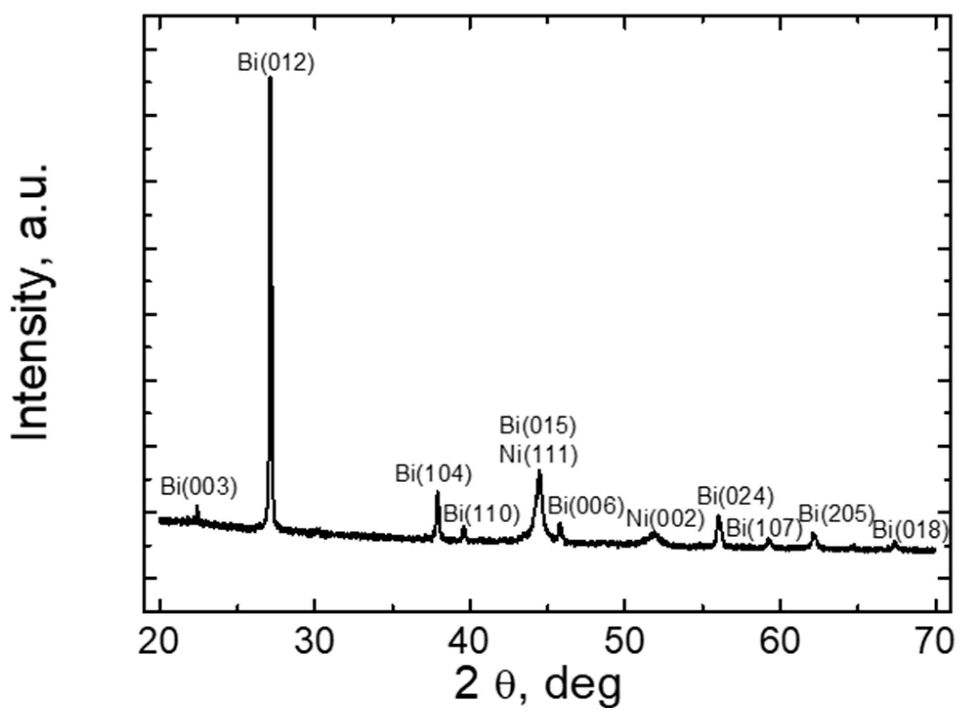
Figure 4 presents the results of XRD studies of the Bi-Ni layer. As the results show, the Bi-Ni layer formed by TEG is polycrystalline. As it can be seen by analyzing the XRD radiographs, a clear spectrum of Bi is obtained. The characteristic peaks of Bi are at 22.5; 27; 38; 39; 44; 46; 56; 59; 62; and 67 degrees. Accordingly, the orientation planes of the Bi polycrystal were determined for each peak, the values of which are given in the XRD radiographs. Meanwhile, characteristic peaks of Ni are observed at 44 and 52 degrees. As we can see at 44 degrees, there is also a spectrum peak characteristic of Bi, so this peak is characteristic for both Bi and Ni elements. Analyzing the spectra, the crystallographic orientations of the planes were also identified in the peaks of the Ni spectrum, the values of which can be found in the Ni spectrogram in
Figure 4. The characteristic peaks of the Ni layer can be observed in the radiographs incomparably less prominently than the peaks characteristic of the Bi layer. This is likely because the Ni layer is composed of very small diameter nanocrystallites that do not have an orderly orientation among themselves.
As the Bi-Ni layer is polycrystalline, this layer structure results in higher electrical conductivity of TEG than in the case of the amorphous structure. Therefore, TEG layers with a polycrystalline structure are more suitable for technological use than the amorphous ones. The XRD study was performed, taking the entire surface area of the TEG. In addition, the XRD study helps to determine whether the layer obtained is composed of pure layers of Bi and Ni metals and whether the metal oxides were formed (metal oxides have a negative effect on the electrical conductivity).
As you know, for a TEG to produce electricity, a temperature difference must be created between two different ends of the metal. During this study, a Bi-Ni layer with a thickness of about 50–100 nm was formed.
Figure 5 shows the results of measuring the temperature difference between the Bi-Ni layers.
As it can be seen from the measurements, the temperature difference between different metals reaches up to 125 K. In addition, the temperature difference was reached quickly enough, within 100 s. This is because metals have a fairly good thermal conductivity, and, as mentioned, these are very thin layers of metals that heated up quite quickly to the chosen maximum temperature difference during this experiment. A rapid onset of temperature difference between metals is a desirable feature, as the TEG begins to operate at maximum capacity to produce electricity. However, at the same time, the good thermal conductivity of metals reduces TEG efficiency. Analyzing the results presented in
Figure 5, it can be seen that the growth of the temperature difference over time is not a uniform process. As mentioned earlier, the Bi-Ni layer was heated using a nichrome heater, but a part of the TEG surface (about 50%) was in contact with the environment (the ambient temperature was close to room temperature). These factors contributed to the uneven growth of the temperature difference over time. The hotter the TEG gets, the more heat it gives off to the environment. Hence, at higher temperatures, the TEG heats up more slowly (as in the case of this study, the growth of the temperature difference slows down sharply when it reaches about 110 K). In real/operating conditions, the growth of the TEG temperature difference is not a monotonic process (and is not described by the dv/dt characteristic).
The goal of using TEGs for electricity generation is to get these devices up and running at maximum capacity as quickly as possible. In other words, so that the TEG reaches the maximum potential difference in the shortest time possible.
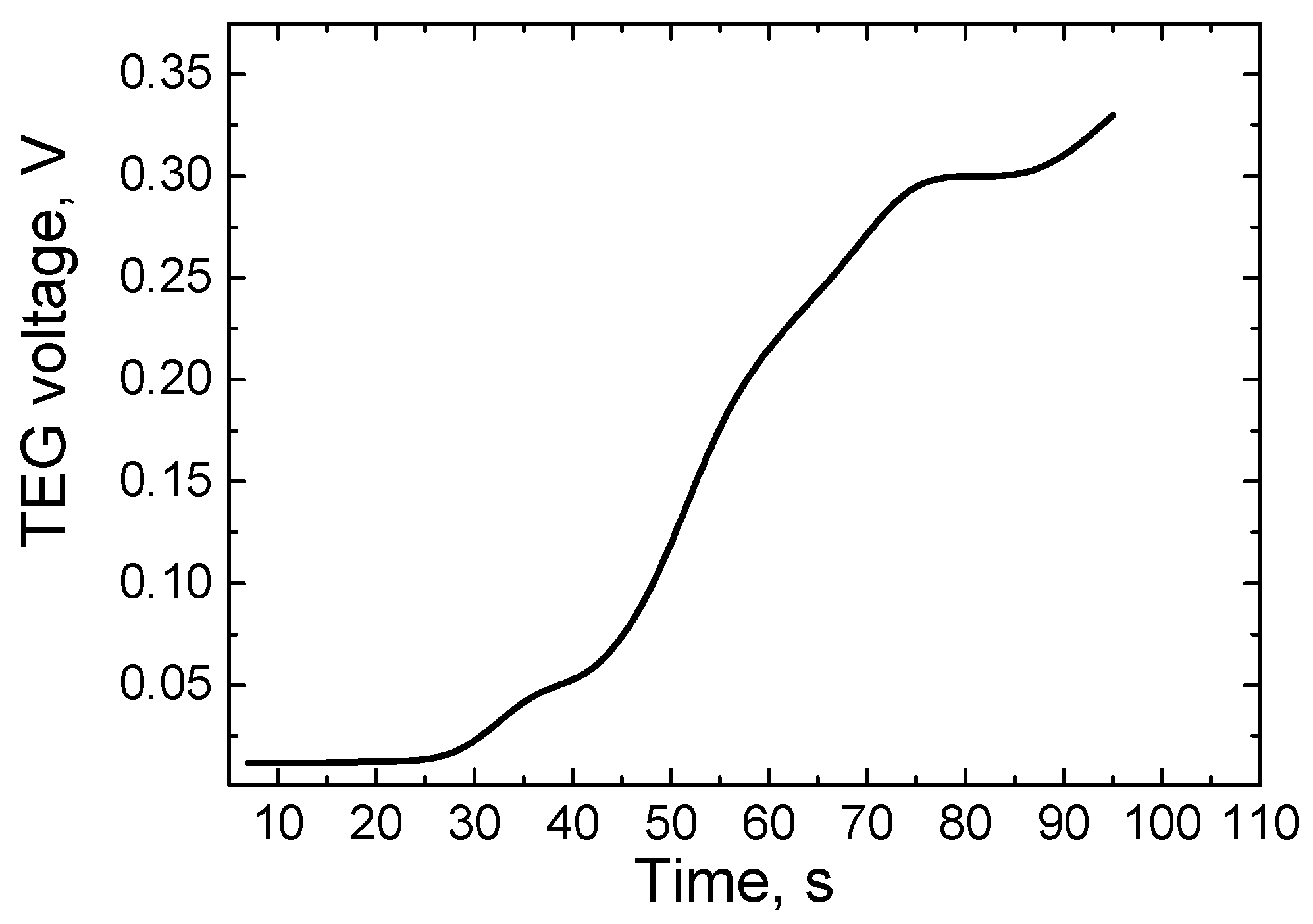
Figure 6 shows the time dependence of the TEG potential difference. As mentioned earlier, the speed at which the TEG reaches its maximum potential difference depends on the thickness of the TEG layers, thermal conductivity, and the external heat source.
As the results of the measurements show, during this study, the maximum potential difference of the TEG used—about 0.35 V—is reached in approximately 100 s. As is known, the potential difference of TEG is partially correlated with the variation of temperature difference. As we can see from the results, the growth of the potential difference over time is not a smooth process, due to the interaction of part of the TEG surface area with the environment. Hence, in real working conditions, the growth of the TEG potential difference over time is not an ideal linear dependence (a part of the TEG surface will always be in contact with a colder environment). In addition, it can be observed that the TEG potential difference begins to grow noticeably after heating for 25 s (which corresponds to a temperature difference of about 80 K). This can be explained by the fact that with such a temperature difference, the electrons in the warm part of the TEG acquire enough kinetic energy and participate in the phenomena of electric current formation.
The electric potential difference of TEG depends on the temperature, but during this research work, we tried to show how this potential difference depends on the heat flux. The dependence of the TEG potential difference on the heat flux is shown in
Figure 7.
As it can be seen from the measurement results, as the heat flux increases from 0 to 4.5 kW/m2, the electrical potential difference increases from 0 to 0.35 V. The greatest change in the growth of the potential difference (from 0.06 to 0.35 V) is observed when the heat flux increases from 2 to 4 kW/m2. Such an uneven growth of the potential difference can be explained by the fact that the active TEG surfaces receive heat from a heat source or radiation by contact. Also, as already mentioned, heat flux transfer to the TEG surfaces depends on the quality of the contact between the TEG surface and the heat source. It can be noticed that with a heat flux higher than 4 kW/m2, the potential difference generated by the TEG does not change. Hence, at this value of the heat flux, the maximum number of accelerated electrons which participate in the process of electric current transfer is reached.
As it is well known, a potential difference (∆U) is formed by the Seebeck mechanism when there is a temperature difference between the different metals that make up the TEG. The dependence of the potential difference on the temperature difference of the formed Bi-Ni layer was measured. The results of the measurement are shown in
Figure 8.
As the research shows, at a temperature difference ranging from 30 to 75 K, the potential difference is minimal, does not change within this temperature range, and reaches about 0.01 V. Meanwhile, a more pronounced increase in the potential difference is observed at a temperature difference of 80 K between the TEG layers, and with an increase in the temperature difference from 80 to 120 K, respectively, the voltage generated by the TEG increases from 0.01 to 0.03 V. Such a change in the potential difference can be explained by the increasing movement of free charge carriers, as the temperature rises between the Bi and Ni layers, and the electric particles move towards the material with a lower electrochemical potential [
1,
2,
3].
The voltage measurement was performed between the Bi and Ni layers. The potential difference of one Bi-Ni junction was measured, for the sake of accuracy, in order to find out the properties of one junction (the aim was to determine how the temperature difference affects the formation of the potential difference in one Bi-Ni junction). Measuring more than one junction leads to measurement distortions, since the total voltage generated by the TEG would be measured, not the individual potential difference of a single TEG junction. Therefore, in order to accurately assess how the temperature difference affects the formation of the potential difference of one junction, it would be impossible to do so by measuring the total generated voltage of many junctions. In addition, when measuring the total voltage (which would be generated by several TEG junctions), it would not be possible to evaluate the characteristic of the Seebeck coefficient because it is evaluated only for one TEG junction, and, in order to evaluate this characteristic, it is necessary to know the dependence of the potential difference of an individual TEG junction on the temperature difference.
During this study, not only the potential difference generated by the TEG was measured, but also the power (measured using a Keithley 5487, a universal instrument for measuring electrical parameters). The dependence of the generated electric power on the temperature difference between the different Bi-Ni layers was also evaluated while studying the operating characteristics of the TEG. These research results are presented in
Figure 9. As it can be seen from the research results, the power generated by the TEG is very low, and as the temperature changes from 70 to 120 K, the generated power increases from 30 to 150 µW. The increase in power generated by a TEG is directly dependent on the change in temperature, which also results in a potential difference. The power of one TEG cell is quite small; this is because only a part of the heat energy falling on the TEG sample is used for the formation of the potential difference. In order to obtain the necessary TEG power (depending on the specific purpose of use), it is necessary to form a battery of TEG cells in which the cells themselves would be connected using a mixed electrical circuit connection [
1,
2,
3,
4]. Various stencil masks can be used for this purpose, when with their help it is possible to deposit not only an individual TEG element, but also to form a whole battery of TEG elements.
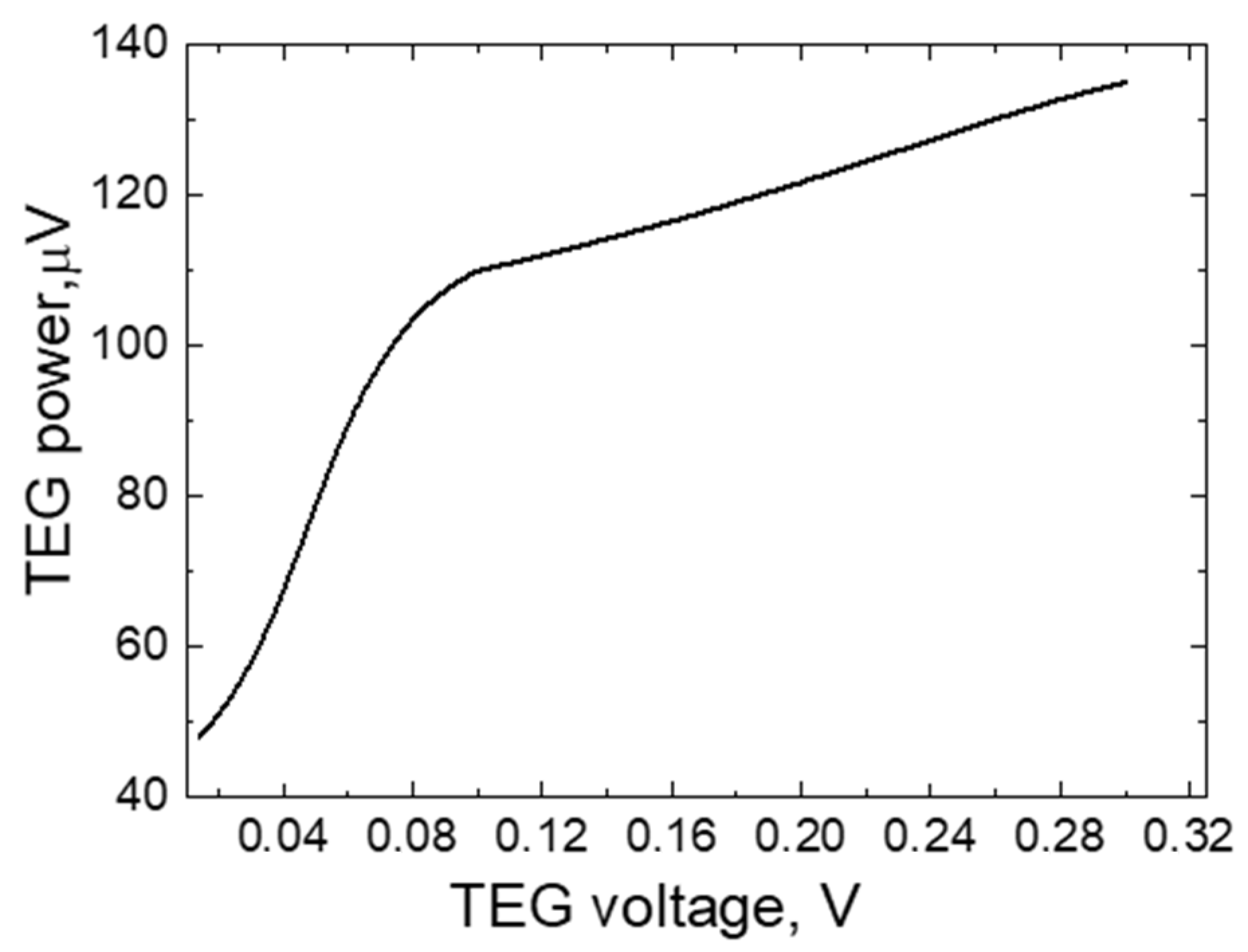
Figure 10 shows the dependence of the power generated by the TEG element on the resulting potential difference. As it can be seen from the results, the power dependence graph consists of two straight lines. The first part of the graph shows that the TEG power increases from 50 to 110 µW when the electric potential difference increases from 0.03 to 0.1 V. Meanwhile, as the voltage increases from 0.01 to 0.3 V, the power increase is slower, from 110 to 135 µW.
Such phenomena are observed because, as the temperature difference between the ends of the TEG increases, the growth in the number of electrical particles slows down. In addition, it can be observed that the interdependence of TEG electrical parameters deviates from Ohm’s law, which is a strictly linear characteristic. This is due to the fact that the number of electrified particles grows non-linearly as the temperature changes [
1,
2].
One of the most important parameters when evaluating the TEG suitability for application is the Seebeck coefficient. The dependence of this parameter on the temperature change is presented in
Figure 11.
The Seebeck coefficient represents the ratio between the potential difference and the temperature change between the TEGs at different ends of the sample. As it can be seen from
Figure 11, the dependence of the Seebeck coefficient on the temperature increase is not linear. This is due to the fact that the number of free electrified particles, on which the potential difference depends, also varies non-linearly. In addition, the literature states that the change in the number of electric free particles is influenced not only by thermodynamic factors but also by quantum phenomena, such as, e.g., the interaction of the metal surface with various electromagnetic fields (when the metal surface interacts with the electromagnetic field, the electrified particles with an elastic connection with atoms are also diluted) [
1,
2,
3]. The suitability of materials for TEG production can be judged from the Seebeck coefficient curve; however, this is not the only characteristic that determines the choice of materials. It is necessary to consider the properties of materials, such as resistance to temperature, thermal expansion properties, etc.
As it is known, the TEG has low efficiency in producing electric current. It is stated in the literature that TEG efficiency varies between 1 and 10% [
1,
2,
3]. The dependence of the efficiency factor of the Bi-Ni-based TEG element on the temperature change is presented in
Figure 12. As the measurements show, efficiency increases from 1 to 4.5% when the temperature change increases from 30 to 119 K.
As it can be seen in this particular case, the efficiency factor of the TEG depends on the temperature change: with a larger temperature change, the TEG works a little more efficiently. Such a dependence of the efficiency factor on the change in temperature is explained (as in the case of electrical characteristics) by the uneven increase in the number of electrified particles as the temperature difference between the ends of different metals increases [
1,
2,
3,
4].
When forming TEGs, the materials for their production are selected taking into account several factors, such as price, prevalence, efficiency, resistance to environmental effects, complexity of formation, physical characteristics, etc.; in other words, the choice of materials depends on the specifics and purpose of the TEG use.


