Article

Influence of the Cadmium Sulfide Chemical Bath Deposition Temperature on Cadmium Sulfide/Zinc Oxide Thin Films

by
Egle Usoviene
,
Neringa Petrasauskiene
*,
Gediminas Jakubauskas
and
Edita Paluckiene
Department of Physical and Inorganic Chemistry, Kaunas University of Technology, Radvilenu 19, 50254 Kaunas, Lithuania
*
Author to whom correspondence should be addressed.
Coatings 2023, 13(7), 1197; https://doi.org/10.3390/coatings13071197
Submission received: 8 June 2023 / Revised: 23 June 2023 / Accepted: 28 June 2023 / Published: 3 July 2023
(This article belongs to the Special Issue Recent Advances in Semiconducting Thin Films)

Abstract

:
The spin-coating method has been employed for nanostructured crystalline zinc oxide (ZnO) thin film preparation on FTO glass substrates. Cadmium sulfide (CdS) layers were then deposited on the surface via the chemical bath deposition method. To investigate the effect of the formation of the CdS layer on ZnO/FTO, the deposition of these layers was performed at three different temperatures (40, 60, and 80 °C). The synthesized CdS/ZnO composite was found to have homogenously distributed crystalline grains of both ZnO and CdS. The uniform distribution of the grains and the equal molar ratio of the two components resulted in excellent optical and photocatalytic performance. Analysis of CdS/ZnO thin films was performed using XRD analysis, UV-vis spectroscopy, scanning electron microscopy, energy-dispersive X-ray spectroscopy, and linear sweep voltammetry. The best optical, morphological, and electrical properties and the highest photocurrent value of the CdS/ZnO thin films were obtained when the CdS layers were formed at 60 °C. X-ray diffraction characterization revealed that CdS/ZnO thin films crystallized into hexagonal wurtzite ZnO and cubic CdS. The crystallite size of ZnO and CdS/ZnO was ~38 nm and ~19 nm, respectively. The band gap calculated for CdS/ZnO, formed at different temperatures, varies from 2.05 to 2.15 eV.

1. Introduction

While developing new material processing techniques, the most common problem that can occur is the use of materials that do not have desirable properties. These problems are often avoided through altering the surface of the material by adding new functional materials. After such operations are performed, the materials can be applied to a wider range of various fields. Although this branch of science is not new, different experimental methods are emerging today, making it possible to achieve ever higher surface electrical conductivity [1,2].
Fluorine-doped tin oxide (FTO) is a transparent oxide that has conductive properties. The band gap values of these substrates range from 3.2 eV to 4.6 eV [3]. Polycrystalline tin oxide operates by absorbing oxygen and trapping electrons on its surface while creating a barrier around this coating. However, when there is a lack of oxygen on the surface, this coating can act as an n-type semiconductor. This phenomenon is explained by the decrease in the ionization level that occurs on the surface. Other factors that determine the conductivity of FTO are impurities and the relative amount of fluorine and tin (F/Sn) on the surface of the substrate [4]. Fluorine-doped tin oxide is used in the production of transparent semiconductors (e.g., ZnO, SnO2, CdS, and CdO). This process improves the optical and electrical properties of the surface [5].
Nanoparticle chemistry is a new branch of science that has emerged in the past 30 years. The concepts used to describe nanoparticles in different fields of science and research often differ, but are generally described as particles that are not larger than 1 to 100 nm in size and whose physical properties would change if the material were composed of larger particles [6]. Zinc oxide nanoparticles have a high exciton binding energy of 60 meV at standard ambient temperature [7,8] and are characterised by high photosensitivity and stability [9]. Because of this, zinc oxide exhibits optical properties that are widely studied for its application in semiconductor photocatalysts [10,11], producing devices that use photons [12]. It is important to note that due to their high surface-to-volume ratio, ZnO nanoparticles increase the number of photogenerated charge carriers [13]. Due to this property, they are often used for various surface coatings [14]. ZnO is an n-type broad direct band gap of ~3.3 eV semiconductor, which means that it can only be activated by UV light, and it is disadvantageous regarding radiation absorption in the visible light region of the solar spectrum [15,16,17]. To enhance the photocatalytic efficiency of ZnO under visible light, it could be essentially combined with visible light sensitizers. It is known that combined nanocrystals or heterostructures exhibit a collective and enhanced property that is distinct from that of any component in them. The heterostructures of different semiconductors can improve the photocatalytic efficiency by mutual transfer of photogenerated charge carriers. In comparison to ZnO, cadmium sulfide possesses a suitable energy band alignment that encourages electron-hole dissociation at the interface and increases the lifetime of the photoexcited charges, thus enhancing the photocatalytic efficiency. Additionally, CdS is photocatalytically active in the visible spectrum due to its narrow band gap (2.4 eV) [18]; Consequently, it has the potential to significantly expand the absorption range of ZnO-CdS heterostructures [19]. The lattice structure of CdS is similar to that of ZnO, so CdS resembles the most suitable visible light sensitizer for ZnO to create a close interaction between the two semiconductors. CdS is a material that exhibits semiconductor properties and is classified as an n-type semiconductor. The excellent thermal and chemical stability makes CdS one of the most important electronic materials in photodetectors and sensors. This material has various electrical properties that depend on the size and temperature of CdS particles [19]. CdS and its thin films are being researched and used in solar cells because of their optoelectronic properties. The efficiency of these solar cells is controlled by thickness variations [20]. The electron transfer process in which photogenerated electrons can flow from CdS to ZnO is promoted by the energy band structure of the materials [21], therefore, achieving a good physical separation of the charge carriers upon their generation.
Combining ZnO and CdS to form the heterostructure should improve their physical and chemical properties. The interface of CdS and ZnO should form a type-II band alignment (Figure 1), which would benefit the electrons transferred from CdS to ZnO, and the holes would be transferred from ZnO to CdS.
Due to the different directions of electron and hole transfer, electron-hole recombination is less likely to occur [22].
In this work, we have introduced a synthesized CdS/ZnO heterostructure on the FTO surface. The ZnO layer was deposited on the FTO substrates via the spin-coating method. The CdS layers were deposited on the ZnO layer using the chemical bath deposition method. These methods are controllable, tunable, simple, and effective. XRD analysis, UV-vis spectrophotometry, scanning electron microscopy, and energy-dispersive X-ray spectroscopy were employed to characterize the features. Finally, we investigated the photocatalytic properties of the samples under ultraviolet and visible light using linear sweep voltammetry.

2. Materials and Methods

2.1. Materials

The bilayer film of the CdS/ZnO structure was deposited on fluorine-doped tin oxide (FTO, TEC 10, Ossila, Sheffield, UK, 3.2 mm thick, 12 Ω/sq,) glass substrates. Commercial zinc oxide nanoparticles (ZnO NP, <100 nm particle size, Sigma-Aldrich, Hamburg, Germany) were used for thin film deposition. The experiments were conducted with freshly prepared solutions without deaeration during the process.
Acetone (CH3COCH3, 99.5%), alcohol (CH3CH2OH, 95%), and all other chemicals used for deposition were purchased from Sigma-Aldrich and were of analytical grade, used without further purification.

2.2. Formation of CdS/ZnO Thin Film

First, the FTO substrates were ultrasonically and sequentially cleaned with nitric acid, acetone, distilled water, and ethanol for 10 min. The FTO substrate was dried in air and then transferred to an oven for 2 h at 100 °C.
To produce the ZnO layer on the FTO substrate, the spin-coating method was used. The suspension of zinc oxide nanoparticles was achieved by ultrasonically dispersing the ZnO nanoparticles in ethanol (0.2 g (ZnO)/10 mL (C2H5OH). The mixture was stirred for 30 min at room temperature to produce a homogeneous suspension. Then, at room temperature, the FTO substrate was spin-coated with the nanoparticle suspension at 3000 rpm for 30 s. The samples were prepared with ten cycles of ZnO nanoparticle deposition. For each cycle, the samples were placed in the oven for 5 min at a temperature of 400 °C to dry before depositing any other layers (Figure 2).
The cadmium sulfide (CdS) layer on ZnO/FTO was grown using the chemical bath deposition technique, as shown in Figure 2. 0.002 M cadmium chloride (CdCl2·2H2O) was complexed with solutions of 0.4 M ammonium chloride (NH4Cl) and 0.02 M ammonia (NH3·H2O), and then mixed with 0.05 M thiourea (CS(NH2)2) as a sulfur source to form a precursor solution for the CdS deposition. The reactions that occur during the formation of the CdS layer are shown below:
CdCl2 + 4NH3·H2O ⟶ [Cd(NH3)4Cl2 + 4H2O,
[Cd(NH3)4Cl2 + CS(NH2)2 + 2HO ⟶ CdS + CH2N2 + 4NH3 + 2H2O.
To investigate the effect of CdS layer formation in different temperature solutions on various properties of CdS/ZnO thin films, solutions at various temperatures were used to form the CdS layer. The ZnO/FTO substrates were immersed in the precursor solution and kept at three different temperatures: 40 °C, 60 °C and 80 °C for 30 min. This process was repeated up to five times (cycles) for the same sample to achieve a higher thickness of the CdS thin film. The prepared samples were washed several times with distilled water, followed by drying at 200 °C for 10 min. The substrates were found to be covered with yellow deposits.

2.3. Characterization of Copper Selenide Films

The crystal phase of the CdS/ZnO samples was examined using an X-ray diffractometer (D8 Advance diffractometer, Bruker AXS, Karlsruhe, Germany). The obtained peaks were identified according to those available in the PDF-2 database. The experimental data values of the zinc oxide and cadmium sulfide lattice spacing d were achieved from the Bragg relation [23] by attributing the θ value of the peak data of the XRD pattern:
n λ = 2 d sin θ
where n (an integer) is the order of diffraction, λ is the wavelength of the incident X-rays, d is the interplanar spacing of the crystal, and θ is the peak position.
The average grain size (D) was calculated based on the full width at the half maximum intensity (FWHM) of the main reflections by applying the Debye Scherrer’s formula [24,25]:
D = 0.9 λ β cos θ
where D is the crystallite size, λ is the X-ray wavelength used, β is the angular line width at half-maximum intensity in radians, and θ is Bragg’s angle.
To perform scanning electron microscopy/energy-dispersive X-ray spectroscopy (SEM/EDX) measurements, a Hitachi S-3400N microscope (Hitachi Ltd., Mito Works, Hitachinaka City, Ibaraki Prefecture, Japan) equipped with the Bruker Quad 5040 EDS system was used.
Atomic force microscopy (AFM) imaging was performed using a NanoWizard 3 NanoScience microscope (JPK Instruments AG, Berlin, Germany).
The optical properties of the CdS/ZnO samples were measured at room temperature using the UV-vis spectrometer SPECTRONIC® GENESYS8 (Perkin Elmer, Waltham, Massachusetts, USA) in the range from 200 to 800 nm. The Tauc plot was used to determine the optical band gap from diffuse absorbance measurements [26,27]:
Ahν = A (hν − Eg)n
where α is the absorption coefficient; hν—photon energy; Eg—energy band gap; A—a constant; n—a constant for a given transition (n = 2 for direct transition). The optical band gap can be estimated from the extrapolation of the linear portion of the (αhν)2 plots versus hν to α = 0.
Linear sweep voltammetry (LSV) for active surface measurements was performed with BioLogic SP-150 (BioLogic Science Instruments, Seyssinet-Pariset, France) potentiostat–galvanostat. EC-Lab® V10.39 software was used for the collection and treatment of experimental data. A standard three-electrode cell (volume 100 mL) was used with platinum wire as the counter electrode, Ag,AgCl|KCl(sat) as the reference electrode, and CdS/ZnO formed on FTO as the working electrode. As the supporting electrolyte, a 0.1 M sodium thiosulfate solution (pH 6.3) was used. During LSV measurements, the potential was swept from −0.4 to +1.0 V in the frequency range of 5 kHz to 50 Hz with a sinus amplitude of 10 mV.

3. Results and Discussion

3.1. Structural Studies

The crystal structures of the CdS/ZnO thin films were determined by the X-ray diffraction pattern. The temperature effect of the solutions used to form the CdS layer on the crystal structure of the CdS/ZnO thin films was investigated. It was observed that the use of different temperature solutions to form CdS resulted in diffractograms with no significant differences in the position of the peaks, their intensities, and full width at half maximum values.
Three sets of diffraction peaks in Figure 3 for the thin film of CdS/ZnO on FTO (the layer of CdS was formed at a temperature of 60 °C) can be attributed to tetragonal rutile SnO2, hexagonal wurtzite ZnO, and cubic CdS, respectively, suggesting its components of ZnO and CdS. The FTO diffraction peaks are located at the 2θ values of 26.78°, 33.96°, 37.98°, 51.75°, 61.99°, and 65.82 (Figure 3a), which correspond to the crystal faces (110), (101), (200), (211), (310) and (301) of tetragonal cassiterite SnO2, respectively. The diffraction peaks confirm the standard card (JCPDS No. 71–0652) and there are no other diffraction peaks except polycrystalline SnO2.
Figure 3b shows the XRD patterns of polycrystalline ZnO formation with characteristic diffraction peaks of hexagonal wurtzite (JCPDS No. 36–1451). Characteristic diffraction peaks of ZnO were observed: 2θ = 31.94°, 34.61°, 36.42°, 47.94°, 57.05°, 63.29°, and 68.37°. The sharpening of these peaks is well defined and narrow; this shows that an asymmetry was formed in the crystalline shapes. This observation is consistent with those of the literature [28,29,30].
The diffractogram of the XRD pattern of the prepared layer of CdS/ZnO (Figure 3c) shows three new broad peaks at values of 2θ = 26.56°, 44.26°, and 54.89° scattered from the planes (111), (220), and (311), respectively, indicating that this composite sample contained ZnO and CdS. These indexed facets agree with the standard JCPDS reference (No.75-0581) [28,29,31,32]. No impurity peak was detected in the XRD patterns, demonstrating the formation of a pure CdS/ZnO thin film. It should be noted that the diffraction peaks observed in the ZnO/FTO structure are sharper, while the diffraction peaks of CdS/ZnO are broader and weaker, which implies the highly crystalline character of ZnO and the small particle size of CdS. The crystal grain size was quantitatively calculated using the Scherrer equation according to the broadening of the diffraction peak in the XRD curves: the grain size of ZnO was ~38 nm, and CdS/ZnO was ~19 nm.
The intensity of ZnO peaks also decreases with the formation of the CdS/ZnO structure. As a result of the significant overlap of the background and peaks, the crystallite size was not calculated. The results of the XRD analysis were compared with the JCPDS data and are given in Table 1.

3.2. Elemental Analysis

To confirm the formation of the CdS layer in the CdS/ZnO thin films, EDX spectroscopy was performed on all samples. The temperature of the solutions used for the formation of the CdS layer was found to have influenced the elemental composition of the thin films of CdS/ZnO (Table 2).
The largest increase in the amount of cadmium can be seen in samples with CdS layers formed at a temperature of 60 °C. The greatest increase in the amount of sulfur can be seen in samples that have CdS layers formed at a temperature of 80 °C. The molar ratio of Cd/S was close to the stoichiometric ratio of CdS (1:1), which confirmed the formation of CdS. With increasing the temperature of deposition of the CdS layer from 60 °C to 80 °C, the value of the molar ratio increases significantly.

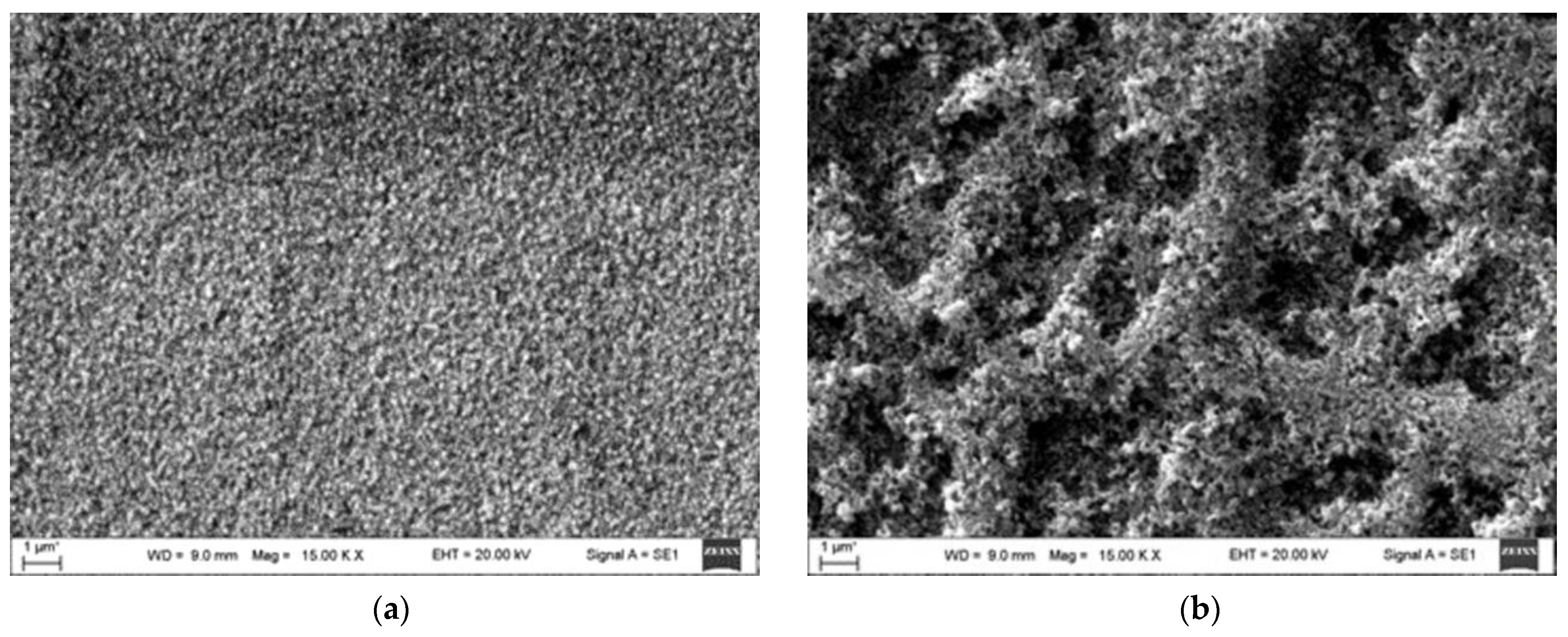
3.3. Morphological Analysis

The morphology of the ZnO layer on FTO and thin films of the CdS/ZnO on FTO was evaluated by SEM and AFM. SEM images of bare FTO and ZnO/FTO are shown in Figure 4. The ZnO layer uniformly covers the FTO substrate, and the surface remains smooth and free of cracks.
The AFM measurements confirmed the findings discussed above. The 2D and 3D images of 10 μm × 10 μm areas of FTO and ZnO/FTO are presented in Figure 5.
To further analyze the surface of the sample, its roughness measurements were taken as well. The results obtained were further investigated by quantifying the parameters of the sample surface. These parameters can be seen in Table 3.
The values of the root mean square (RMS) roughness Rq, the average roughness A, and RMS peak to valley roughness Rsk decrease when the ZnO nanoparticle layer is deposited on FTO glass, indicating that the ZnO structure becomes smoother (Table 3).
The SEM images show the crystalline structure of CdS/ZnO thin films obtained by using different CdS layer formation conditions, using different chemical bath temperatures (Figure 6).
An increase in the temperature of CdS deposition was found to form a denser layer of CdS/ZnO, composed of tightly packed grains that form agglomerates with diameters ranging from 200 nm (80 °C) to 1 μm (40 °C).
During the formation of CdS/ZnO layers, it was found that the films prepared at a temperature of 60 °C (Figure 6b) are quite dense, have good crystallinity, and are more compact than the CdS/ZnO films prepared at a temperature of 40 °C. (Figure 6a). It can be seen that a crystalline structure prevails at a temperature of 40 °C, which acquires a dense dendritic structure when the temperature is raised to 80 °C (Figure 6c). The height and surface morphology of the CdS/ZnO thin film formed on the surface of the FTO depend on the deposition temperature: at different deposition temperatures, the microstructures of the thin films differ. The surface images obtained show a rough film surface with particles gathered in agglomerates. A more compact and denser surface, with greater uniformity and homogeneity than the other surfaces, is obtained by the deposition of CdS at 60 °C (Figure 7c).
As can be seen, the thin film of CdS/ZnO deposited in a solution at a temperature of 60 °C has the lowest values of the morphological parameters given in Table 3.

3.4. Optical Analysis

To investigate the optical properties, the UV-vis absorption spectra of the ZnO and CdS/ZnO thin films prepared on a FTO substrate were measured. ZnO demonstrates strong absorption in the ultraviolet region with a spectral wavelength of around 400 nm (Figure 8).
After the deposition of the CdS layer on ZnO, the absorption peak shifted to the visible region. This indicates that the CdS/ZnO semiconductor has the appropriate band gap for visible light activation to improve the photocatalytic efficiency [10,30,31]. The results illustrated in Figure 8 show a higher absorption intensity peak for CdS/ZnO compared to that of ZnO. This confirms that the thin film structure is composed more of CdS and less of ZnO in amount [10].
As shown in Figure 9, the band gap value calculated for ZnO is 3.2 eV, which corresponds to the value in the literature (~3.3 eV) [15,16,17]. The band gap calculated for CdS/ZnO, formed at different temperatures, varies from 2.05 to 2.15 eV and appears to be independent of the deposition conditions.
Shifts towards the visible light region can be the cause of the quantum confinement effect observed on CdS/ZnO semiconductors. These results show that the CdS layer effectively increases the photoabsorption capacity of ZnO in the visible region [33]. Therefore, it is expected that the extended photoresponse range and well-matched band edges in the heterostructure would be widely applicable in the field of photocatalysis, allowing a higher proportion of visible light for photocatalytic reactions and achieving higher efficiencies in the separation of electron-hole pairs.

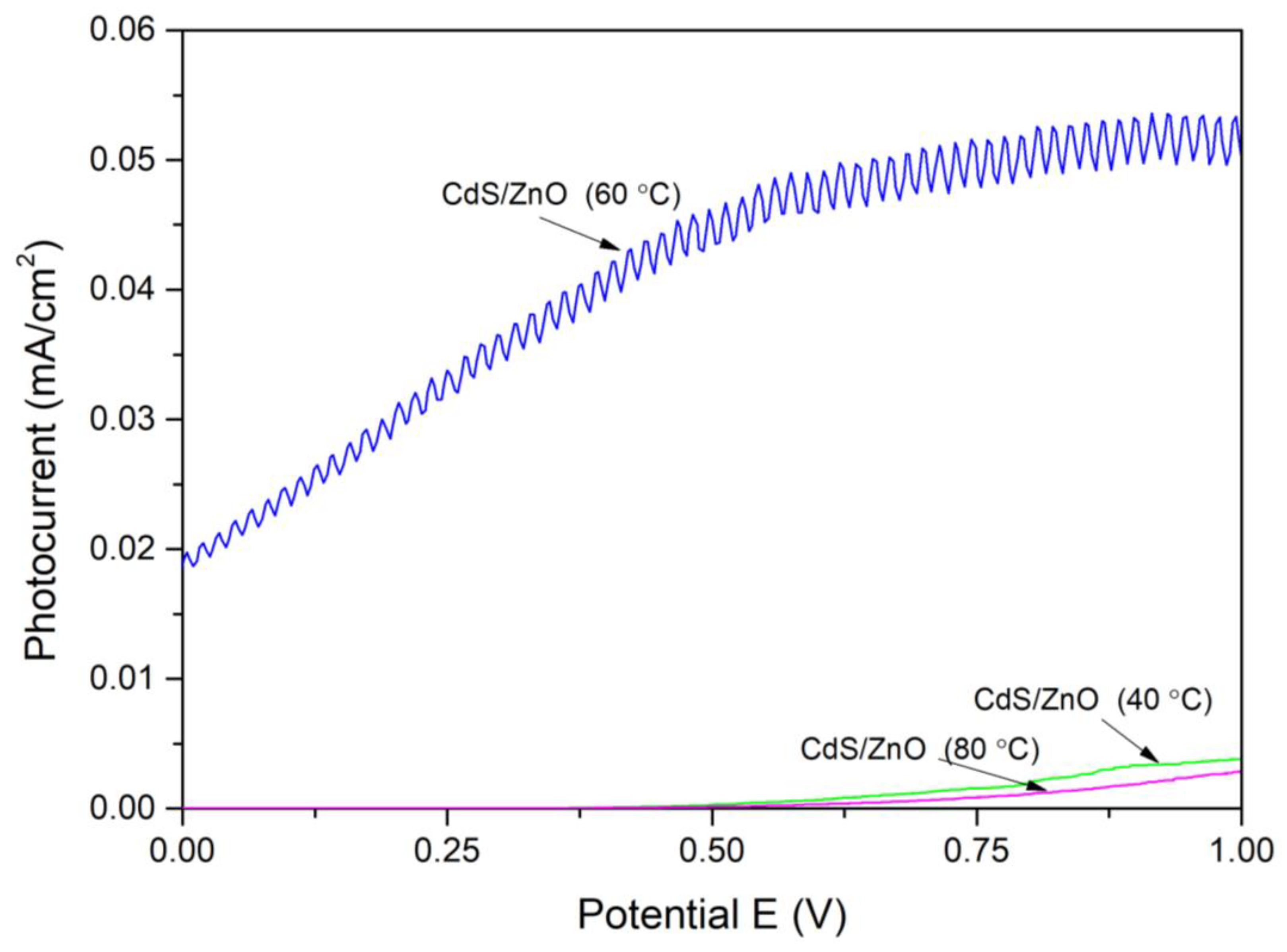
3.5. Electrochemical Analysis

The linear sweep voltammetry (LSV) study of the thin film CdS/ZnO is shown in Figure 10. One of the most important properties of semiconductors is the change in electrical conductivity when light is added to them. This analysis allows us to fully characterize the semiconduction properties of the thin films obtained by using measurements of the photoelectrochemical conductivity by polarization in the dark and exposure to ultraviolet radiation in a 0.1 M Na2S2O3 electrolyte solution. LSV results show that all samples exhibit current density values in the dark and in ultraviolet radiation at 1.0 V (Table 4).
The dependence of the photocurrent variation on the potential of the CdS/ZnO thin film formed at three different temperatures is shown in Figure 10.
The highest photocatalytic efficiency was demonstrated when a thin CdS/ZnO film was formed at 60 °C.

4. Conclusions

CdS/ZnO thin films were successfully prepared on the FTO substrate. The ZnO layer was deposited on the FTO substrate via the spin-coating method, and the CdS layer was deposited on the ZnO layer using the chemical bath deposition method.
The CdS/ZnO thin films were thoroughly characterized by different standard techniques. To investigate the effect of CdS layer formation in different temperature solutions on the properties of CdS/ZnO thin films, the deposition was performed at three different temperatures (40, 60, and 80 °C). The best optical, morphological, and electrical properties and the highest photocurrent value of the CdS/ZnO thin films were obtained when the CdS layers were formed at 60 °C. The XRD pattern showed that the crystalline phases of the CdS/ZnO thin films consist of hexagonal wurtzite ZnO and cubic CdS. The crystallite size of ZnO and CdS/ZnO was ~38 nm and ~19 nm, respectively. The SEM and AFM analysis exposed that the grains combined into agglomerates with diameters from 200 nm (80 °C) to 1 μm (40 °C). A more compact and denser surface, with greater uniformity and homogeneity than the other surfaces, is obtained by deposition of CdS at 60 °C. The value of the direct band gap of the ZnO layer on the FTO obtained with UV-vis spectroscopy was 3.2 eV. The band gap calculated for CdS/ZnO, formed at different temperatures, varies from 2.05 to 2.15 eV and appears to be independent of the deposition conditions. The elemental analysis confirmed that the CdS crystals were close to the stoichiometric ratio. The highest photocatalytic efficiency was demonstrated when the CdS/ZnO thin film was formed at 60 °C. Because of the uniformly distributed grains and the molar ratio of the two components being equal, excellent optical and photocatalytic performance was demonstrated by the thin films.

Author Contributions

Conceptualization, E.P. and E.U.; methodology, E.P. and E.U.; validation, E.P. and E.U.; formal analysis, N.P., E.U. and E.P.; investigation, E.U. and G.J.; data curation, E.P. and N.P.; writing—original draft preparation, E.U. and N.P.; writing—review and editing, N.P. and E.P.; visualization, G.J. and E.U.; supervision, E.P. and N.P. All authors have read and agreed to the published version of the manuscript.

Funding

This research received no external funding.

Institutional Review Board Statement

Not applicable.

Informed Consent Statement

Not applicable.

Data Availability Statement

Not applicable.

Conflicts of Interest

The authors declare no conflict of interest.

References

  1. Mozetič, M. Surface Modification to Improve Properties of Materials. Materials 2019, 12, 411. [Google Scholar] [CrossRef] [PubMed] [Green Version]
  2. Pelevin, I.A.; Ozherelkov, D.Y. Special Issue: Surface Modification of Engineering and Functional Materials. Coatings 2022, 12, 1016. [Google Scholar] [CrossRef]
  3. Ramírez-Amador, R.; Flores-Carrasco, G.; Alcántara-Iniesta, S.; Rodríguez González, J.; García-Teniza, O.; Mercado-Agular, E.; Vásquez-Ortiz, A.B. Structural, Morphological, Optical, and Electrical Characterization of Fluorine Doped Tin Oxide (FTO) Thin Films Synthesized by PSP. Solid State Phenom. 2019, 286, 64–71. [Google Scholar] [CrossRef]
  4. Moholkar, A.V.; Pawar, S.M.; Rajpure, K.Y.; Patil, P.S.; Bhosale, C.H. Properties of Highly Oriented Spray-Deposited Fluorine-Doped Tin Oxide Thin Films on Glass Substrates of Different Thickness. J. Phys. Chem. Solids 2007, 68, 1981–1988. [Google Scholar] [CrossRef]
  5. Kucukomeroglu, T.; Bacaksiz, E.; Terzioglu, C.; Varilci, A. Influence of Fluorine Doping on Structural, Electrical and Optical Properties of Spray Pyrolysis ZnS Films. Thin Solid Films 2008, 516, 2913–2916. [Google Scholar] [CrossRef]
  6. Yokoyama, T.; Masuda, H.; Suzuki, M.; Ehara, K.; Nogi, K.; Fuji, M.; Fukui, T.; Suzuki, H.; Tatami, J.; Hayashi, K.; et al. Basic Properties and Measuring Methods of Nanoparticles. In Nanoparticle Technology Handbook; Elsevier: Amsterdam, The Netherlands, 2008; pp. 3–48. [Google Scholar]
  7. Pearton, S.J.; Norton, D.P.; Ip, K.; Heo, Y.W.; Steiner, T. Recent Progress in Processing and Properties of ZnO. Superlattices Microstruct. 2003, 34, 3–32. [Google Scholar] [CrossRef]
  8. Di Bartolomeo, A.; Zin Toe, M.; Kian Tan, W.; Muto, H.; Kawamura, G.; Matsuda, A.; Aisha Binti Yaacob, K.; Pung, S.-Y. Effect of Carrier Gas Flow Rates on the Structural and Optical Properties of ZnO Films Deposited Using an Aerosol Deposition Technique. Electron. Mater. 2022, 3, 332–343. [Google Scholar] [CrossRef]
  9. Fang, X.; Bando, Y.; Gautam, U.K.; Zhai, T.; Zeng, H.; Xu, X.; Liao, M.; Golberg, D. ZnO and ZnS Nanostructures: Ultraviolet-Light Emitters, Lasers, and Sensors. Crit. Rev. Solid State Mater. Sci. 2009, 34, 190–223. [Google Scholar] [CrossRef]
  10. Li, B.; Wang, Y. Synthesis, Microstructure, and Photocatalysis of ZnO/CdS Nano-Heterostructure. J. Phys. Chem. Solids 2011, 72, 1165–1169. [Google Scholar] [CrossRef]
  11. Hoffmann, M.R.; Martin, S.T.; Choi, W.; Bahnemann, D.W. Environmental Applications of Semiconductor Photocatalysis. Chem. Rev. 1995, 95, 69–96. [Google Scholar] [CrossRef]
  12. Willander, M.; Nur, O.; Fakhr-e-Alam, M.; Atif, M.; AlSalhi, M.S. ZnO Nanostructures: Toxicity and Phototoxicity Characteristics in Biological Samples. In Zinc Oxide Nanostructures: Advances and Applications; Jenny Stanford Publishing: Dubai, United Arab Emirates, 2014; pp. 157–184. ISBN 9789814411349. [Google Scholar]
  13. Bao, Q.; Liu, X.; Xia, Y.; Gao, F.; Kauffmann, L.D.; Margeat, O.; Ackermann, J.; Fahlman, M. Effects of Ultraviolet Soaking on Surface Electronic Structures of Solution Processed ZnO Nanoparticle Films in Polymer Solar Cells. J. Mater. Chem. A 2014, 2, 17676–17682. [Google Scholar] [CrossRef] [Green Version]
  14. Sypniewska, M.; Szczesny, R.; Popielarski, P.; Strzalkowski, K.; Derkowska-Zielinska, B. Structural, Morphological and Photoluminescent Properties of Annealed ZnO Thin Layers Obtained by the Rapid Sol-Gel Spin-Coating Method. Opto-Electron. Rev. 2020, 28, 182–190. [Google Scholar] [CrossRef]
  15. Hameed, T.A.; Sharmoukh, W.; Anis, B.; Youssef, A.M. Enhanced Photocatalytic Activity and Diode Performance of ZnO-GO Nanocomposites via Doping with Aluminum. Int. J. Energy Res. 2022, 46, 22601–22624. [Google Scholar] [CrossRef]
  16. Xu, F.; Volkov, V.; Zhu, Y.; Bai, H.; Rea, A.; Valappil, N.V.; Su, W.; Gao, X.; Kuskovsky, I.L.; Matsui, H. Long Electron—Hole Separation of ZnO-CdS Core—Shell Quantum Dots. J. Phys. Chem. C Nanomater. Interfaces 2013, 113, 19419–19423. [Google Scholar] [CrossRef]
  17. Weinhardt, L.; Heske, C.; Umbach, E.; Niesen, T.P.; Visbeck, S.; Karg, F. Band Alignment at the I-ZnO/CdS Interface in Cu(In,Ga)(S,Se) 2 Thin-Film Solar Cells. Appl. Phys. Lett. 2004, 84, 3175–3177. [Google Scholar] [CrossRef]
  18. Sadovnikov, S.I.; Rempel, A.A.; Gusev, A.I. Nanostructured Lead, Cadmium, and Silver Sulfides; Springer Series in Materials Science; Springer International Publishing: Cham, Switerland; Berlin/Heidelberg, Germany, 2018; Volume 256, pp. 127–188. ISBN 978-3-319-56386-2. [Google Scholar]
  19. Murray, C.B.; Norris, D.J.; Bawendi, M.G. Synthesis and Characterization of Nearly Monodisperse CdE (E = S, Se, Te) Semiconductor Nanocrystallites. J. Am. Chem. Soc. 1993, 115, 8706–8715. [Google Scholar] [CrossRef]
  20. Supekar, A.; Kapadnis, R.; Bansode, S.; Bhujbal, P.; Kale, S.; Jadkar, S.; Pathan, H. Cadmium Telluride/Cadmium Sulfide Thin Films Solar Cells: A Review. ES Energy Environ. 2020, 10, 3–12. [Google Scholar] [CrossRef]
  21. Wu, Y.; Tamaki, T.; Volotinen, T.; Belova, L.; Rao, K.V. Enhanced Photoresponse of Inkjet-Printed ZnO Thin Films Capped with CdS Nanoparticles. J. Phys. Chem. Lett. 2010, 1, 89–92. [Google Scholar] [CrossRef]
  22. Tak, Y.; Hong, S.J.; Lee, J.S.; Yong, K. Fabrication of ZnO/CdS Core/Shell Nanowire Arrays for Efficient Solar Energy Conversion. J. Mater. Chem. 2009, 19, 5945–5951. [Google Scholar] [CrossRef] [Green Version]
  23. Bragg, W.H.; Bragg, W.L. The Reflection of X-Rays by Crystals. Proc. R. Soc. Lond. Ser. A Contain. Pap. A Math. Phys. Character 1913, 88, 428–438. [Google Scholar] [CrossRef]
  24. Patterson, A.L. The Scherrer Formula for X-Ray Particle Size Determination. Phys. Rev. 1939, 56, 978. [Google Scholar] [CrossRef]
  25. Nath, D.; Singh, F.; Das, R. X-ray Diffraction Analysis by Williamson-Hall, Halder-Wagner and Size-Strain Plot Methods of CdSe Nanoparticles—A Comparative Study. Mater. Chem. Phys. 2020, 239, 122021. [Google Scholar] [CrossRef]
  26. Tauc, J.; Grigorovici, R.; Vancu, A. Optical Properties and Electronic Structure of Amorphous Germanium. Phys. Status Solidi 1966, 15, 627–637. [Google Scholar] [CrossRef]
  27. Makuła, P.; Pacia, M.; Macyk, W. How To Correctly Determine the Band Gap Energy of Modified Semiconductor Photocatalysts Based on UV-Vis Spectra. J. Phys. Chem. Lett. 2018, 9, 6814–6817. [Google Scholar] [CrossRef] [Green Version]
  28. Lam, K.-T.; Hsiao, Y.-J.; Ji, L.-W.; Fang, T.-H.; Hsiao, K.-H.; Chu, T.-T. High-Sensitive Ultraviolet Photodetectors Based on ZnO Nanorods/CdS Heterostructures. Nanoscale Res. Lett. 2017, 12. [Google Scholar] [CrossRef] [Green Version]
  29. Lavand, A.B.; Malghe, Y.S. Visible Light Photocatalytic Degradation of 4-Chlorophenol Using C/ZnO/CdS Nanocomposite. J. Saudi Chem. Soc. 2015, 19, 471–478. [Google Scholar] [CrossRef] [Green Version]
  30. Adegoke, K.A.; Iqbal, M.; Louis, H.; Bello, O.S. Synthesis, Characterization and Application of CdS/ZnO Nanorod Heterostructure for the Photodegradation of Rhodamine B Dye. Mater. Sci. Energy Technol. 2019, 2, 329–336. [Google Scholar] [CrossRef]
  31. Sankhla, A.; Sharma, R.; Yadav, R.S.; Kashyap, D.; Kothari, S.L.; Kachhwaha, S. Biosynthesis and Characterization of Cadmium Sulfide Nanoparticles—An Emphasis of Zeta Potential Behavior Due to Capping. Mater. Chem. Phys. 2016, 170, 44–51. [Google Scholar] [CrossRef]
  32. Kim, J.I.; Kim, J.; Lee, J.; Jung, D.-R.; Kim, H.; Choi, H.; Lee, S.; Byun, S.; Kang, S.; Park, B. Photoluminescence Enhancement in CdS Quantum Dots by Thermal Annealing. Nanoscale Res. Lett. 2012, 7, 482. [Google Scholar] [CrossRef] [Green Version]
  33. Zou, Z.; Xie, C.; Zhang, S.; Yang, C.; Zhang, G.; Yang, L. CdS/ZnO Nanocomposite Film and Its Enhanced Photoelectric Response to UV and Visible Lights at Low Bias. Sens. Actuators B Chem. 2013, 188, 1158–1166. [Google Scholar] [CrossRef]
Figure 1. Band diagram of the ZnO-CdS interface.
Coatings 13 01197 g001
Figure 2. Steps of preparation of CdS/ZnO thin films on FTO.
Coatings 13 01197 g002
Figure 3. X-ray diffraction patterns of (a) bare FTO, (b) ZnO/FTO, and (c) CdS/ZnO/FTO.
Coatings 13 01197 g003
Figure 4. SEM images of (a) bare FTO and (b) ZnO/FTO.
Coatings 13 01197 g004
Figure 5. AFM images of (a) bare FTO and (b) ZnO/FTO.
Coatings 13 01197 g005
Figure 6. SEM images of thin films of CdS/ZnO formed at different temperatures: (a) 40 °C; (b) 60 °C; (c) 80 °C.
Coatings 13 01197 g006
Figure 7. Topographic images of CdS/ZnO thin films formed at different temperatures: (a) 40 °C; (b) 60 °C; (c) 80 °C.
Coatings 13 01197 g007
Figure 8. UV-vis spectra.
Coatings 13 01197 g008
Figure 9. A plot of (αhν)2 versus Photon energy.
Coatings 13 01197 g009
Figure 10. Dependence of photocurrent variation on the potential for thin CdS/ZnO films formed at temperatures of 40 °C, 60 °C, and 80 °C.
Coatings 13 01197 g010
Table 1. XRD data of CdS/ZnO and comparison with JCPDS data of observed d values with standard d values.
Peaks Assigned to MaterialsAnalysis ResultsJCPDS Data
2θd, Ǻd, ǺMiller Indexes (hkl)PDF No.Crystalline Phase
FTO26.783.333.35(110)71-0652Cassiterite SnO2 tetragonal
33.962.642.64(101)
37.982.372.37(200)
51.751.771.76(211)
61.991.501.49(310)
65.821.421.42(301)
ZnO31.942.802.81(100)36-1451Wurtzite ZnO hexagonal
34.612.592.60(002)
36.422.462.48(101)
47.941.891.91(102)
57.051.611.62(110)
63.291.471.47(112)
68.371.371.38(201)
CdS26.563.353.37(111)75-0581CdS cubic
44.262.042.02(220)
54.8931.671.68(311)
Table 2. Dependence of the amount of elements on different temperatures during the formation of the CdS layer.
CdS Layer Forming TemperatureAmount of Elements Wt, %Molar Ratio of Cd/S
CdS
40 °C48.1316.721.22
60 °C51.0617.831.22
80 °C30.3017.792.06
Table 3. Morphology parameters of CdS/ZnO on FTO surface.
ParametersSmooth Part of Sample
A, nmRq, nmRsk, nm
Cleaned FTO glass substrate12.615.9143.3
ZnO/FTO11.514.5124.5
CdS/ZnO/FTO40 °C118.9150.21158.0
60 °C84.55107.7882.2
80 °C104.1135.81250.0
Table 4. LSV results of CdS/ZnO thin films at a potential value of 1.0 V.
CdS Forming TemperatureSample Surface Area A, cm2Current Density juv Value Achieved Using UV Radiation, mA/cm2Current Density jt Value Achieved in the Dark, mA/cm2juv/jtPhotocurrent jphoto, mA/cm2
40 °C1.050.0040.00075.710.003
60 °C1.050.0580.00658.920.052
80 °C0.70.0030.000215.000.003
Disclaimer/Publisher’s Note: The statements, opinions and data contained in all publications are solely those of the individual author(s) and contributor(s) and not of MDPI and/or the editor(s). MDPI and/or the editor(s) disclaim responsibility for any injury to people or property resulting from any ideas, methods, instructions or products referred to in the content.

