1. Introduction
Wear-resistant coatings substantially increase the service life of metal-cutting tools [
1]. They improve the characteristics of the tools, such as hardness, wear resistance, oxidation resistance, and reduce the coefficient of friction [
2,
3]. However, when the coating wears out, it should be removed to facilitate resharpening and recoating. The removal of wear-resistant coatings is a difficult task because of their strong adhesion and small thickness.
One of the widely used methods for removing coatings is the chemical method based on the use of various acid solutions. The tool is placed in acid to dissolve the worn or defective coating. The use of hazardous chemicals imposes additional safety precautions and increases the risk of industrial accidents. The disposal of used solutions is one of the main problems of this method [
4].
The majority of currently used cutting tools have their cutting edges modified with wear-resistant PVD (physical vapor deposition) coatings [
5]. The more expensive coated tools are reused several times after resharpening and recoating. The basic process is the grinding of the tool rake face. Without the removal of the worn-out coatings, it is impossible to carry out more than two such grindings. Coating stripping is more difficult because of the variety of both substrate and coating materials [
6]. The structure and properties of different types of PVD coatings deposited on various tool materials are presented in [
7,
8,
9]. The coating’s efficient removal requires the retention of a proper substrate surface. This problem was tackled in recent investigations of numerous materials: high speed steels, cemented carbides, oxide and mixed ceramics [
10,
11,
12].
Chemically stripped substrates may have a roughness similar to that of the coated material [
13,
14]. The disadvantages of chemical methods are long stripping times and large volumes of toxic waste. These problems can be resolved using electrochemical dissolution, which is both faster and safer for the environment [
15].
For the rapid and high-quality removal of AlTiN [
16] and other coatings, a laser beam can be used. Laser stripping is a more ecologically friendly, effective method, which is associated with minimal damage to the substrate [
17]. In [
18], the coating was deposited on a disc sample with a diameter of 25 mm and a thickness of 4.4 mm. The disc was mirror polished with a diamond paste containing 3 µm grains, yielding a final surface roughness of Ra = 0.005 μm. A solid state Nd:YAG pulsed laser was used to strip the coatings. This laser with a spot diameter of 0.18 mm has a wavelength of 1064 nm and a pulse duration of 120 ns, with a repetition rate ranging from 1 to 50 kHz. According to measurements using energy dispersive spectroscopy, approximately 20%–30% of the coating elements were detected on the stripped surfaces. The reason is that pulsed laser stripping causes the melting and mixing of tools and coating materials, which makes it difficult to separate and remove the coating thus lengthening the process.
In addition, the laser removal of coatings demonstrates the quite uneven surface of treated samples. One of the reasons for this is the small value of the laser spot diameter, ~0.1 mm. Melting and evaporation in subsequent points of the coated sample result in a wavy surface with a wavelength comparable to that of the laser spot diameter. To avoid this, it needs to act on the surface with a broad beam of uniformly distributed particles. The particles might be accelerated ions or fast neutral atoms.
There exist a lot of ion sources, which produce beams with circular cross-sections [
19]. The beam diameter can amount to 38 cm [
20] or even reach 50 cm [
21]. The plasma emitter of ions is produced in a gas discharge chamber with thermionic cathodes. Ions are accelerated from the emitter by an ion optical system consisting of two or three parallel grids. The ion beam current can reach several amperes at the ion energy and up to several keV.
The sources with thermionic cathodes cannot produce ions of reactive gases. Therefore, ion sources with plasma emitters generated in a gas discharge with a cold, hollow cathode were developed [
22,
23]. As the positive ions are able to charge the surfaces of any substrates under processing, and sometimes provoke undesirable defects in the superficial layer, it is reasonable to use sources of fast neutral atoms [
24,
25,
26] instead of ion sources.
The fast neutral atoms appear due to charge exchange collisions of accelerated ions with gas atoms. For instance, at room temperature and a gas pressure of
p = 0.2 Pa, the mean free path λ of argon atoms is equal to 0.04 m [
27]. When the energy of argon ions increases from 0.5 to 6 keV, their charge exchange cross-section σ
c decreases from 3 × 10
−19 to 1.7 × 10
−19 m
2 [
28,
29]. Neglecting the gas heating in the discharge, we may suppose that at
p = 0.2, the Pa density of argon atoms amounts to
no = 5 × 10
19 m
−3 and the charge exchange length λ
c = 1/
noσ
c of argon ions increases from 0.07 to 0.12 m with ion energy increasing from 0.5 to 6 keV. This means that the number of elastic collisions between argon atoms exceeds the number of charge exchange collisions with accelerated ions by two or three times. However, this does not prevent fast atoms from efficiently sputtering the substrate at a rate proportional to their energy and flux density onto the substrate surface.
The sputtering rate is one of the important parameters that determine the applicability of fast atoms for coating removal. From a practical point of view, the processing time should not exceed the time of ~10–20 min needed to evacuate a working vacuum chamber after loading tools therein. Therefore, to remove the AlTiN coating with a thickness of 3 μm within 20 min, the etching rate should be about 10 μm/h. The present study proved the achievability of these parameters using the compression of a beam of fast argon atoms.
Unlike all previous methods for removing worn coatings, the innovations of this study are the acceptable removal rate and the ability to sharpen the cutting edges of cleaned tools before applying new coatings.
2. Materials and Methods
2.1. Experimental Setup
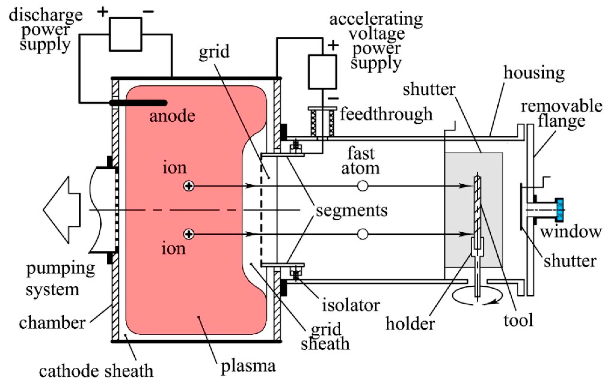
Figure 1 shows an experimental setup for the removal of wear-resistant coatings. It is composed of a 50 cm diameter and a 30 cm long cylindrical vacuum chamber and rectangular housing, which communicate with each other through a rectangular opening in the chamber wall. The housing length amounts to 50 cm; its width and height are equal to 40 cm and 30 cm, respectively. The height of the opening between the chamber and the housing is equal to 22 cm and its width is equal to 32 cm. The opposite end of the housing is closed with a removable flange. The housing and chamber are evacuated by a turbomolecular pump through a grounded flat grid on the chamber wall, which prevents the plasma from penetrating into the pump. An anode is mounted inside the chamber and is connected to the positive pole of a discharge power supply.
In the opening between the chamber and the housing, a 31 cm wide and 21 cm high accelerating grid, shaped as a part of 80 cm diameter hollow cylinder with a vertical axis, is mounted (
Figure 2).
The grid is made of a 1 mm thick titanium sheet perforated with 7.2 mm diameter orifices, with the distance between their centers amounting to 8 mm. From above and below, it is rigidly attached to two 6 mm thick, 31 cm wide and 7 cm long titanium plates. The 3 cm long part of the plate, adjacent to the grid, is a segment of an 80 cm diameter circle and the remaining 4 cm long part of the plate is a rectangle. The plates are fastened to the top and bottom of the housing with pairs of ceramic isolators protected from deposition of metal films with hollow screens. Through a high-voltage feedthrough the grid is connected to negative pole of accelerating voltage power supply. It provides negative voltage on the grid ranging from 0.1 to 6 kV.
The gas pressure in the chamber is measured by MKS-vacuummeter with transducer BARATRON (MKSI, Andover, MA, USA) and regulated with a two-channel gas supply system. Inside the housing at a distance of 40 cm from the accelerating grid is positioned a rotating holder for a cutting tool, which should be stripped of wear-resistant coating. The rotation speed amounts to 60 rpm. To fix the tool on the holder, it is necessary to temporarily remove the removable flange. There is on the flange a quartz window with a movable shutter preserving the window from deposition of metal films. It is used for in-situ measuring of the tool temperature using an infrared pyrometer. Near the rotating holder on both sidewalls of the housing two planar magnetrons are mounted. The magnetron targets width is equal to 10 cm and their length amounts to 20 cm. One of the targets is made of titanium and the other is made of aluminum. The magnetron targets are distant from the rotating holder at 10 cm and equipped with movable shutters preserving them from deposition of stripped coating material.
When at the gas pressure of 0.2 Pa the discharge power supply is switched on, the gas discharge is ignited and both the chamber and the housing are filled with discharge plasma [
30,
31]. After the accelerating voltage power supply is switched on, an increase in the voltage
U between the chamber and the grid leads first to growth of the current in the grid circuit
Ig and then to a sharp fall of the current (
Figure 3) accompanied with extinction of plasma glow in the housing. At higher voltage
U the grid prevents penetration of electrons from the chamber to the housing, and the housing is not involved more in discharge. The current in the grid circuit
Ig is equal to the total current of ions extracted from plasma and secondary electrons emitted by the grid, and it keeps a constant value. Since at voltages lower than 600 V, the coefficient of ion-electron emission does not exceed 0.1 [
32], the secondary electron current can be neglected, and
Ig may be considered as the current of ions arriving from the plasma to the grid. Only at the voltage
U exceeding 1 kV the current
Ig can rise again.
Plasma in the chamber is separated from the grid and chamber walls with sheaths of positive space charge. According to the Child–Langmuir law [
33] the sheath width on the grid is equal to
where ε
o is the electric constant equal to 0.885 × 10
−11 F/m,
e is the electron charge,
M is the ion mass,
U is the grid voltage,
Ud is the discharge voltage and
j is the ion current density. When the ion mass
M = A
MA is measured in atomic mass units A = 1.66 × 10
−27 kg, the sheath width is equal to
When at a constant discharge current Id the grid voltage increases, ions from the plasma are accelerated in the grid sheath and pass through the grid orifices into the housing. The grid transparency amounts to η = 0.75 and about 25% of accelerated ions strike the grid and cause secondary emission of electrons from its surface. The emitted electrons are accelerated in the grid sheath and strike the chamber thus increasing the ion current from its walls. It leads to a noticeable decrease in discharge voltage from Ud = 400 V to Ud = 350 V at U = 6000 V. The chamber surface area is equal to S = 0.69 m2, the grid surface area is equal to Sg = 0.07 m2 and at the discharge current Id = 2 A the ion current density j = Id/(S + Sg) = 2/0.86 = 2.32 A/m2. At Ud = 350 V, U = 6000 V and j = 2.32 A/m2 the cathode sheath width amounts to 0.3 cm and the grid sheath width amounts to d = 4.4 cm.
As the charge exchange length λ
c = 1/
noσ
c of argon ions with energy of 6 keV at the gas pressure of 0.2 Pa amounts to 0.12 m and exceeds the grid sheath width by 3 times, we may suppose that all fast argon atoms appear in the housing and arrive to the holder (
Figure 2) with energies of
e(
U +
Ud) = 6.35 keV.
The ion sputtering rate of a substrate is equal to
where
Y is sputtering coefficient, equal to the ratio of the number of atoms leaving the substrate to the number of ions bombarding its surface,
j is the ion current density,
e is electron charge,
M is the mass of one substrate atom, and ρ is density of the substrate material. The coefficient
Y depends mainly on the type of ions, their kinetic energy and on the substrate material [
34].
For example, when sputtering an iron substrate with ρ = 7.9 × 10³ kg/m3 and M = 9.2 × 10⁻²⁶ kg by ions with energy of 6 keV, the sputtering coefficient is equal to Y = 4 and at j = 2.32 A/m2 and e = 1.6 × 10⁻¹⁹ C the sputtering rate is equal to v = Y (j/e) (M/ρ) = 4 × (2.32/1.6 × 10−19) (9.2 × 10⁻²⁶/7.9 × 103) = 0.675 nm/s = 1.93 µm/h. Fast atoms sputter materials with the same intensity as their ions with equal kinetic energy. Consequently, fast argon atoms cannot provide the required coating removal rate, which should exceed 10 µm/h.
An increase in the rate of wear-resistant coating removal is possible due to compression of a broad beam of fast argon atoms formed by concave accelerating grid (
Figure 2). After accelerated from the plasma ions crossed the grid with a surface curvature radius of 40 cm, they move to the focal line of cylindrical grid distant at 40 cm. At the initial width of the beam equal to 30 cm its reduction to 1.5 cm would signify twentyfold increase in the etching intensity.
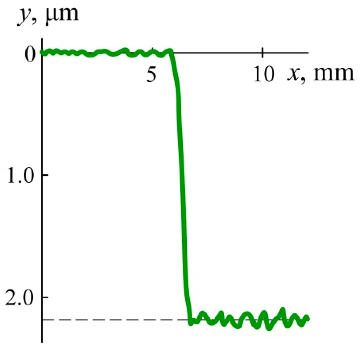
To obtain the distribution of the fast atoms’ flux over the beam width, 2 mm thick and 25 mm wide titanium targets with lengths of 10, 14, 22 and 34 cm were in turn installed inside the housing at distances from the accelerating grid of 35, 30, 20 and 5 cm. The polished target surface facing the grid was covered along its entire length with a mask made of a 10 mm wide titanium strip. After the target was etched with a beam and cooled in a vacuum, it was taken off from the housing and the mask was removed. Using a Dektak XT stylus profilometer, transverse profilograms of the target surface were obtained. The measurement of the height of a step between the profilogram sections, corresponding to the open surface of the target sputtered with fast atoms and the surface covered with a mask, gives the thickness of the layer removed by fast atoms. Dividing the thickness of the removed layer by the processing time gives the etching rate.
2.2. Characterization of the Samples
For in situ measurement of the sample temperature, an infrared pyrometer IMPAC IP 140 (LumaSense Technologies GmbH, Frankfurt am Main, Germany) was used.
To obtain profilograms for measuring the depth of an etched section of a target surface, a Dektak XT stylus profilometer manufactured by Bruker Nano, Inc. (Billerica, MA, USA) was used.
The cutting edges were controlled using an optical 3D measuring system, MicroCAD premium+ (GFMesstechnik GmbH, Teltow, Germany).
The microhardness of the samples was measured using the Micro Indentation TesterMNT produced by Anton Paar Switzerland AG (Buchs, Switzerland).
The characterization of the coating adhesion was carried out using the Nanovea M1 Hardness and Scratch Tester produced by Nanovea Inc. (Irvine, CA, USA).
The elemental analysis of substrate material was provided by a VEGA3 LMH scanning electron microscope (Tescan, Brno, Czech Republic).
The roughness of the tool surface was evaluated using the HOMMEL TESTER T8000 high-precision profilograph/profilometer produced by the company Hommelwerke GmbH (JENOPTIK Industrial Metrology Germany GmbH, Jena, Germany).
3. Results
Solid carbide twist drills with cylindrical shanks and solid carbide helical end mills with cylindrical shanks were chosen as samples to carry out the experiments. The drill diameter amounts to 10 mm, its length to 105 mm and the cutting length to 60 mm. On the drill surface, a titanium nitride coating was deposited, with a thickness of about 3 µm. The end mill length is equal to 100 mm, the diameters of its cutting part and shank to 10 mm, the length of the cutting part to 40 mm and the shank length to 44 mm. On the cutting parts of the end mills, an AlTiN coating was deposited, with a thickness amounting to about 3 µm.
Figure 4 shows the profilogram of a titanium target surface. The target was a 34 cm long titanium strip, distant at 5 cm from the accelerating grid. Two sections are visible on the profilogram, corresponding to the surface, which was covered by the mask (left), and the surface sputtered over half an hour due to fast argon atoms. The height of the step between the sections is equal to the thickness of the removed titanium layer, 2.2 μm. Dividing the thickness of the removed titanium layer by the time of its sputtering by fast argon atoms, we obtain the etching rate v = 4.4 μm/h.
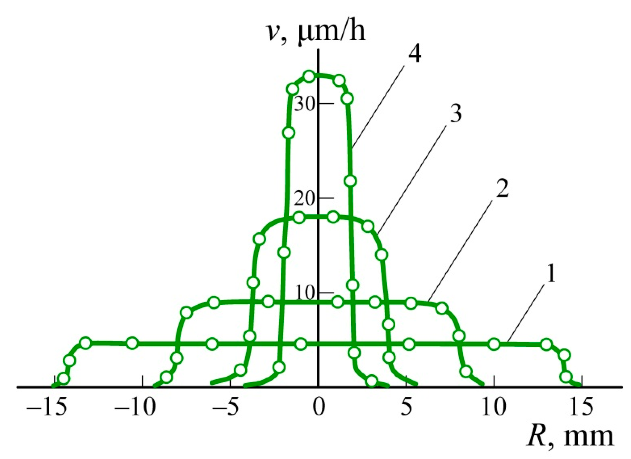
Figure 5 shows distributions of the target etching rate by a converging beam formed in the housing by the concave grid. The distributions were obtained at argon pressure
p = 0.2 Pa, current in the chamber circuit
Id = 2 A and accelerating voltage
U = 6 kV, at a distance from the grid of
h = 5 cm (1), 20 cm (2), 30 cm (3) and 35 cm (4). At the distance
h = 5 cm, the etching rate keeps a constant value of v = 4.4 μm/h over the entire beam width of 28 cm. At
h = 35 cm, the beam width decreases to 4 cm, and the etching rate grows to v = 33 μm/h.
When a drill with a 3 µm thick titanium nitride coating was fixed on the holder (
Figure 1) and sputtered with fast argon atoms, it was possible to observe the drill through the quartz window on the removable flange. Within 15 min, the goldish TiN coating disappeared in the drill slots, and 5 min later the coating was removed from the entire surface of the drill.
A cylindrical mask was put on the top of another drill before etching it with fast argon atoms. After 20-minute-long etching, the mask was removed from the drill, and a distinct boundary was seen between the surface of the drill with the removed coating and the surface covered by the mask during the etching (
Figure 6).
Measurements using an optical 3D measuring system MicroCAD premium + showed that due to etching the drill with fast argon atoms, the radius of its side edge decreased on average by 3 μm, i.e., the thickness of the removed titanium nitride coating. The drill etching was carried out at argon pressure p = 0.2 Pa, discharge current in the anode circuit Id = 2 A and voltage on the grid U = 6 kV. It took only 20 min to remove the 3 μm thick titanium nitride coating from the drill surface. It turned out that the thickness of titanium nitride coating deposited on the drill edges exceeded the coating thickness in slots. Therefore, it took more time to remove the coating from the drill edges than from its slots.
When a 100 mm long and 10 mm diameter end mill with a 3 µm thick AlTiN coating was etched on the same rotating holder (
Figure 1), the observation through the window revealed that the processes had similar features. At argon pressure
p = 0.2 Pa, discharge current
Id = 2 A and voltage on the grid
U = 6 kV, the coating disappeared first in slots of the end mill and it took 25 min to remove the AlTiN coating from its entire surface.
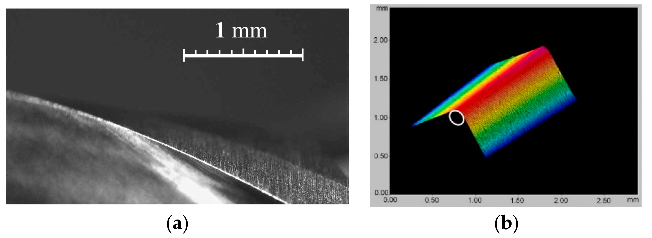
Before the end mill etching, the radii of its cutting edges were measured at the distances of 5 mm (zone A), 20 mm (B) and 35 mm (C) from the mill end. At each distance, the cutting-edge radius was measured in three radial sections distant from each other at 0.1 mm. The MicroCAD premium+ system makes it possible to obtain profiles of the surface in any cross-section of the cutting edge (
Figure 7a) and to measure the radius of the inscribed circle (
Figure 7b), which is equal to the cutting-edge radius.
The cutting-edge radius was measured in three zones A, B and C, distant at 5, 20 and 35 mm from the mill end. Its value was found in each zone as the arithmetic mean of the measured values for three sections distant from each other at 0.1 mm. The average value of the cutting-edge radius in zone A, distant from the mill end at 5 mm, was equal to
RA = 13.8 μm (
Figure 8); the cutting-edge radius in zone B, distant from the mill end at 20 mm, was equal to
RB = 14.2 μm; the cutting-edge radius in zone C was equal to
RC = 13.6 μm.
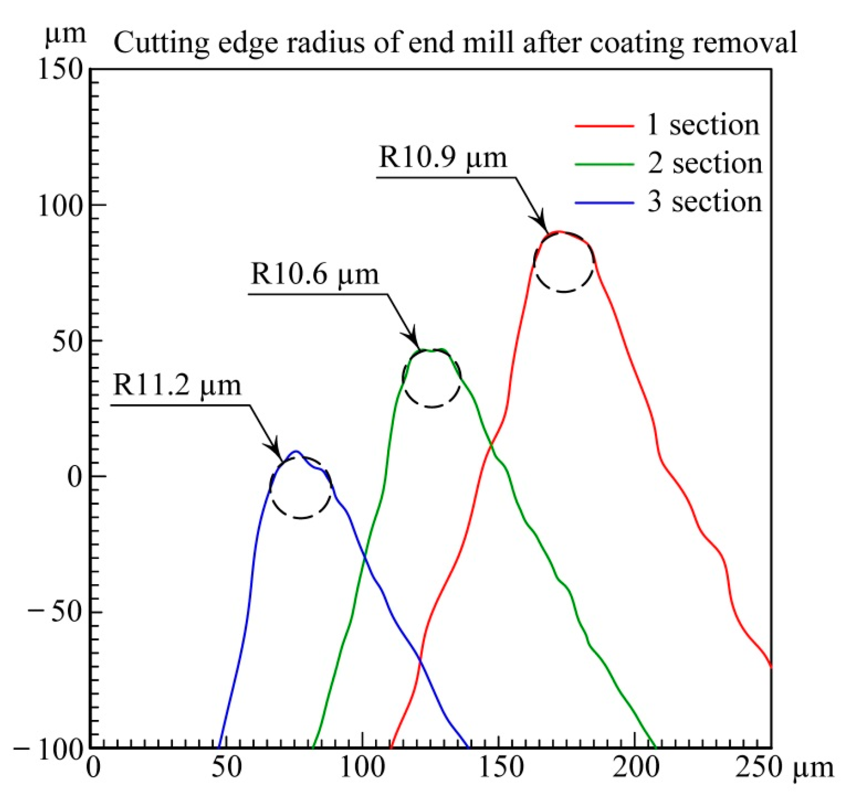
After etching the end mill for 25 min, the color of its cutting part changed and became indistinguishable from the color of the shank. The elemental analysis of the etched surface using a VEGA3 LMH scanning electron microscope has not revealed traces of aluminum and titanium. This means that the AlTiN coating has been completely removed. The measurement of the cutting-edge radius showed that in zone A, distant from the etched mill end at 5 mm, it was equal to
RA = 10.6 μm; in zone B, distant from the etched mill end at 20 mm, the cutting-edge radius was equal to
RB = 10.9 μm (
Figure 9); and in zone C, distant at 35 mm, it was equal to
RC = 10.4 μm. The temperature of the end mill, measured during the removal of the coating, did not exceed 700 °C.
Then, the end mill without a wear-resistant coating was again mounted on a rotating holder and etched with fast argon atoms for one hour at an argon pressure of
p = 0.2 Pa, a discharge current of
Id = 2 A and a grid voltage of
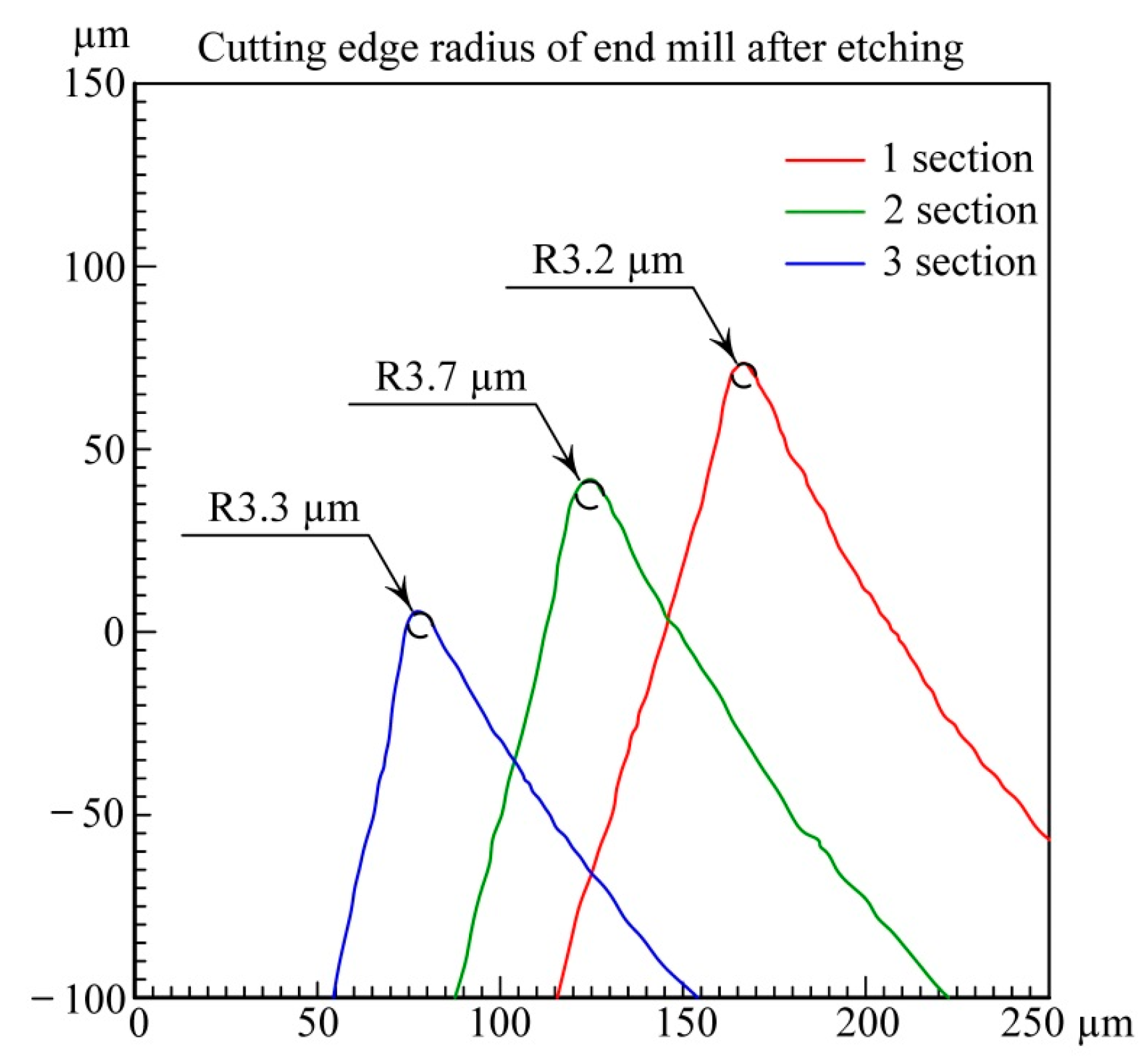
U = 6 kV. To estimate the etching rate, a mask was attached to the shank of the end mill before the etching. After the etching, the mask was removed and the height of the step between sections of the shank profilogram, corresponding to masked and open surfaces of the shank, was measured using a HOMMEL TESTER T8000 high-precision profilometer. Dividing the step height of 7.6 μm by the etching time gives the etching rate of 7.6 μm/h. After the etching, the cutting-edge radius in zone A distant from the etched mill end at 5 mm was equal to
RA = 3.6 μm; in zone B distant from the etched mill end at 20 mm the cutting-edge radius was equal to
RB = 3.5 μm; and in zone C distant at 35 mm it was equal to
RC = 3.4 μm (
Figure 10).
Thus, etching for one hour with 6 kV argon atoms of an end mill without a wear-resistant AlTiN coating led to a decrease in the radius of its cutting edges by 7 μm from 10.6 to 3.5 μm, and to the removal of a 7.6 μm thick superficial layer from the end mill shank.
The end mill with sharpened cutting edges has again been placed on the rotating holder for the deposition of a new wear-resistant coating. To evaluate the coating thickness, a mask was attached to the shank of the end mill. Before deposition, the tool was heated and its surface was activated for 5 min with fast argon atoms at a gas pressure
p = 0.2 Pa, a discharge current
Id = 2 A and a grid voltage
U = 6 kV. Then, 30% nitrogen was added to argon, the discharge current was reduced to 0.5 A and the grid voltage was reduced to 1 kV. After the shutters of both aluminum and titanium magnetron targets were open, the magnetron power supplies were switched on with stabilized currents of 6 A. During the two-hour deposition process, the growing coating was exposed to fast argon and nitrogen atoms.
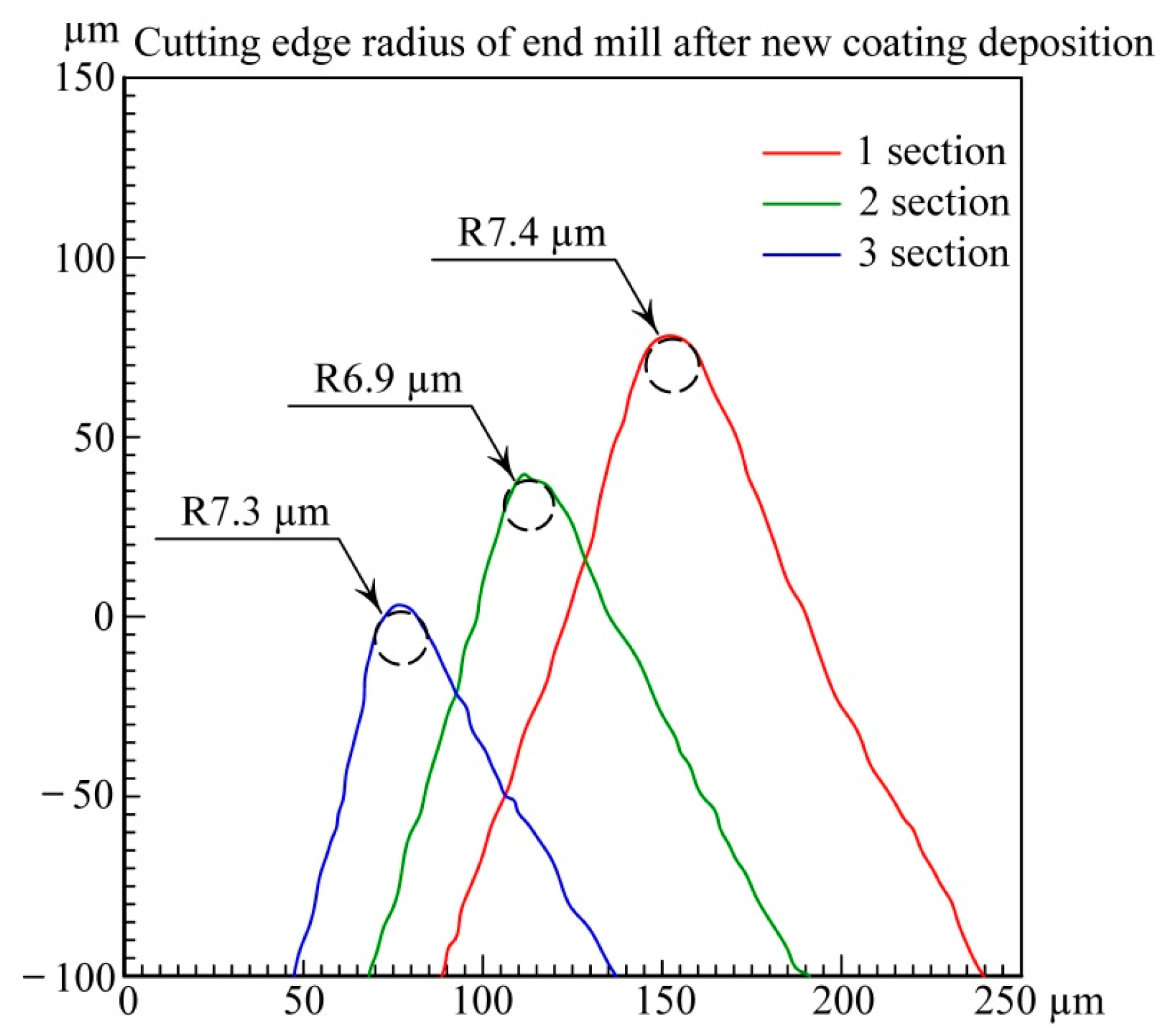
Figure 11 presents the results of the cutting-edge radii measurements in zone A of the end mill with a new coating.
The temperature of the end mill, measured with an infrared pyrometer IMPAC IP 140 during the new coating deposition, amounted to 420 °C. The average value of the cutting-edge radius in zone A, 5 mm away from the end of the cutter with a new coating, was equal to
RA = 7.2 µm; in zone B, distant from the mill end at 20 mm, the cutting-edge radius was equal to
RB = 7.1 μm; and in zone C, distant at 35 mm, it was equal to
RC = 7.0 μm. The evolution of the cutting-edge radii due to the removal of a wear-resistant coating, sharpening the cutting edges by fast argon atoms and the deposition of a new coating, is presented in
Table 1.
With the help of a high-precision profilometer HOMMEL TESTER T8000, it was found that the roughness of the end mill after one-hour-long etching increased slightly, from Ra = 0.22 μm to Ra = 0.24 µm.
An increase of 3.6 μm in the cutting-edge radius after the deposition of a new coating is in good agreement with the thickness of the coating deposited on the end mill shank, which amounts to 4 μm. The thickness was measured as the height of the step on a profilogram of the shank surface without the mask, which was taken off after the new coating’s deposition.
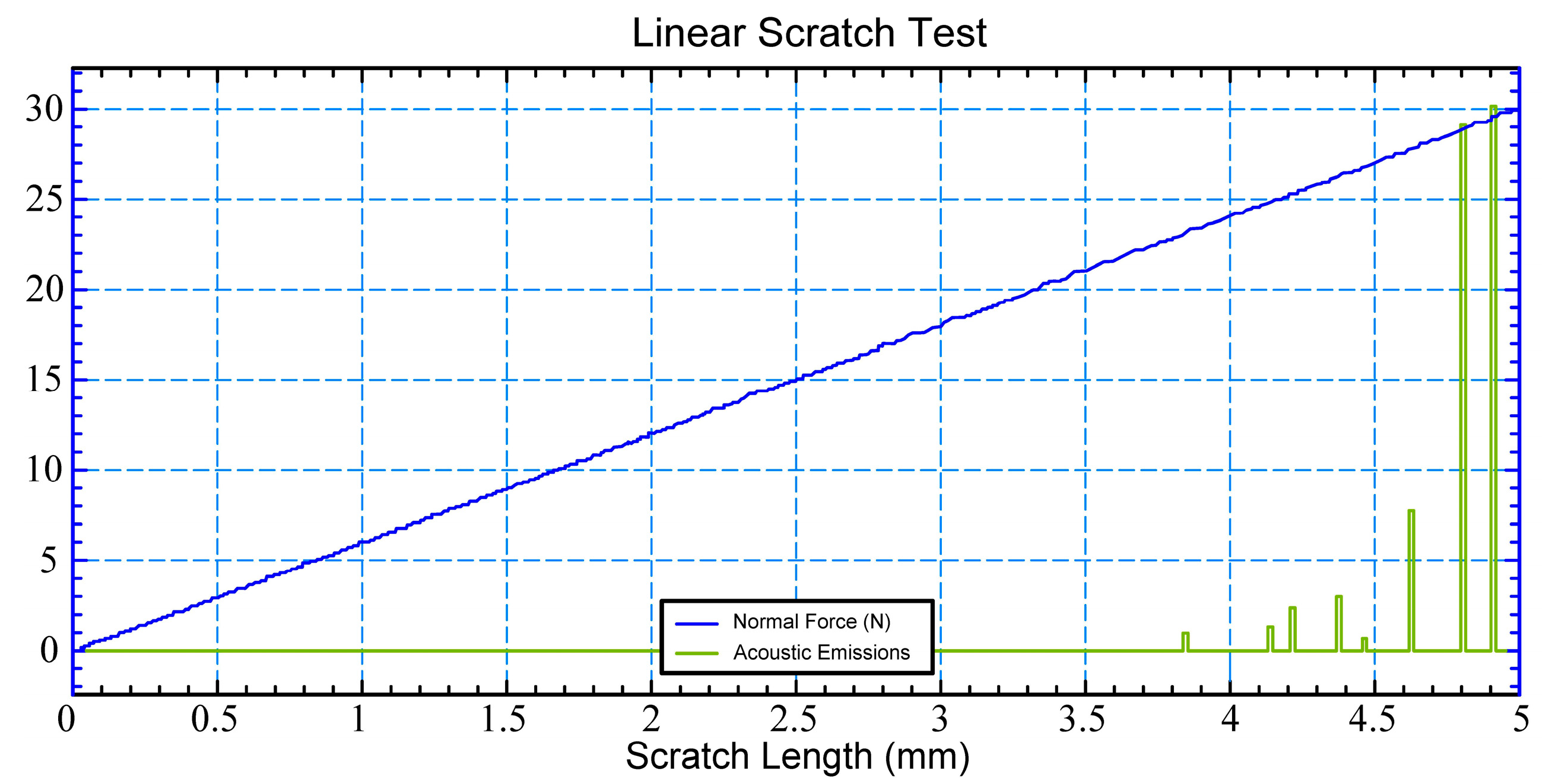
The coating microhardness measured using the Micro Indentation TesterMNT amounted to 2300 HV40, which is close to the microhardness of the original coating before removal. To measure the coating adhesion, a Hardness and Scratch Tester was used. The first critical load, resulting in the appearance of an acoustic emission and the first cracks on the coating, amounted to Lc1 = 29 N (
Figure 12), which is better than for the original coating with Lc1 = 25 N.
The fairly good adhesion is due to the continuous bombardment of the tool surface by the fast particles during the deposition [
35,
36,
37].
4. Discussion
The above results demonstrate a new capability of fast neutral atom beams [
38,
39] to be used in the technology of wear-resistant coating removal from cutting tools and other articles. The processing of a 10 mm diameter solid carbide helical end mill by a beam of argon atoms with an energy of 6 keV resulted in the removal of a 3 µm thick AlTiN coating after 25 min. During processing, the tool was heated by the beam to approximately 700 °C, which is quite acceptable for carbide tools.
Moreover, additional processing of the cleaned end mill for one hour more led to a significant sharpening of its cutting edges. The reason for this is the homogeneous sputtering of the tool’s surface by fast argon atoms. They sputter the cutting edges of the rotating end mill with the same intensity as the rest of its surface. When removing a surface layer of uniform thickness, the cutting-edge radius decreases. It allowed the redeposition of a 3.5 µm thick AlTiN coating and thus we obtained a coated end mill with a cutting-edge radius of 7 µm, which is suited to environmentally friendly dry technological machining systems [
40]. Of course, it is not necessary after the wear-resistant AlTiN coating’s removal to deposit the same kind of coating. The coating could be TiN, CrN, TiZrN or something else; it is only needed to replace the aluminum and titanium targets with magnetron targets made of necessary materials.
To generate a plasma emitter of ions, non-self-sustained discharge with thermionic and hollow cathodes [
41] or a discharge with plasma confinement [
42] can be used. Both are related to plasma generation using hollow cathode [
43]. In our research, a 50 cm diameter and 30 cm long cylindrical vacuum chamber of the experimental setup were used as a big hollow cathode. Due to the electrostatic confinement of electrons inside the chamber, the glow discharge plasma is maintained at a low gas pressure of ~0.1 Pa. The reason is that electrons emitted by the chamber walls are accelerated by the cathode fall of potential between the chamber and plasma and are reflected back by the cathode fall near the opposite wall of the chamber. Before reaching the surface of the anode immersed in the plasma, an electron can be reflected hundreds of times. Its path through the plasma is equal to
L = 4
V/
Sa, where
V is the chamber volume, and
Sa is the anode surface area [
30]. At the chamber volume
V = 0.06 m
3 and the anode surface area
Sa = 0.0048 m
2, the electron path length is equal to
L = 50 m.
Due to more than one hundred reflections in the cathode fall region, the electrons emitted from the chamber walls are uniformly distributed in the chamber volume. They uniformly ionize the gas in the chamber, which determines the uniform distribution of the plasma density. This ensures a fairly uniform distribution of the ion current density on the concave accelerating grid (
Figure 2). In all known ion beam sources [
19,
20,
21,
22,
23], the accelerating voltage of positive polarity is applied to the plasma emitter. In those sources, the gas discharge chamber, the discharge power supply and other systems are subjected to high voltage, and special measures are required to prevent electrical breakdowns.
Breakdown problems are much easier to solve when a high voltage of negative polarity is applied only to the accelerating grid. However, this method has some peculiarities. At a low voltage on the accelerating grid, the gas discharge plasma fills both the chamber and the housing. An increase in the grid voltage is accompanied by an increase in the width of the space charge sheath between the grid and the plasma. This leads to an increase in the surface area of the plasma emitting ions to the grid, and to an approximately twofold increase in the grid current (
Figure 3). When the width of the sheath reaches the radius of the grid openings equal to 3.6 mm, the grid cuts off the plasma in the chamber and prevents its electrons from penetrating into the housing. At this time, a sharp drop in the grid current occurs, accompanied by the extinction of the plasma glow in the housing. At higher voltages, the housing is not involved in discharge and the grid current keeps a constant value equal to the total current of ions extracted from plasma located in the chamber.
Thus, a concave grid at a negative voltage of more than 1 kV is capable of forming compressed beams of fast atoms in the housing adjacent to a chamber filled with a plasma emitter. In our case, the twentyfold compression of a 30 cm wide beam of fast argon atoms with an energy of 6 keV made it possible to remove a 3 µm thick AlTiN coating from a 10 mm diameter solid carbide helical end mill after 25 min. Without compression, it would take more than four hours. The additional processing of a cleaned end mill for one hour more allows for a significant sharpening of its cutting edges and, after the deposition of a new coating, for obtaining a cutting tool with improved machining capability. To expand the scale of application of the new technique and the possibilities of its application in industry, it is necessary to develop systems for the simultaneous processing of several tools in one batch.
In further studies, it is necessary to expand the possibilities of compressed beams of fast argon atoms for cutting tools made of dielectric ceramics.
