1. Introduction
Innovative photoelectric detection applications of low-dimensional nanomaterials have attracted extensive attention due to their ability to lower power consumption and extend the lifetime of detection equipment and due to their light-trapping effect, making them suitable for anti-reflection coatings [
1,
2,
3]. Silicon nanowire arrays, as promising materials, provide special large-area surface textures for strongly increasing the absorption of incident light in the visible to infrared region and have been successfully exploited as high-performance photodetectors to rapidly and accurately detect light waves that exist in the current environment. Therefore, SiNWs exhibit scalable applications with large industrial infrastructures for low-cost and high-yield processing in various technological fields, such as biosensors, self-powered ultraviolet photodetectors, photovoltaic devices and lithium-ion batteries [
4,
5,
6,
7,
8]. In recent years, various methods have been reported for synthetizing one-dimensional nanomaterials. Electrochemical synthesis using inorganic molten salts as electrolytes has achieved great success in assembling nanomaterials, as well as the extraction of other active metals. Simon Schweidler et al. [
9] studied the degradation behavior of a high-entropy oxyfluoride cathode material in lithium cells during electrochemical cycling in situ via acoustic emission monitoring. Yifan Dong et al. [
10] developed a more sustainable method to produce silicon nanowires in bulk quantities through the direct electrochemical reduction of CaSiO
3. Takashi Okazoe et al. [
11] reported the synthesis of a perfluoropolyether derivative that possesses –(CF
2CF
2O)– as a repeating unit. However, the synthesis process of materials can be affected by many external experimental factors, such as process conditions, as well as the ionic concentration of the electrolyte. Last year, Gao Sen et al. [
12] prepared highly dense and vertically aligned sub-5 nm silicon nanowires with length/diameter aspect ratios greater than 10,000 by developing a catalyst-free chemical vapor etching process and successfully observed an unusual lattice reduction of up to 20% within ultra-narrow silicon nanowires.
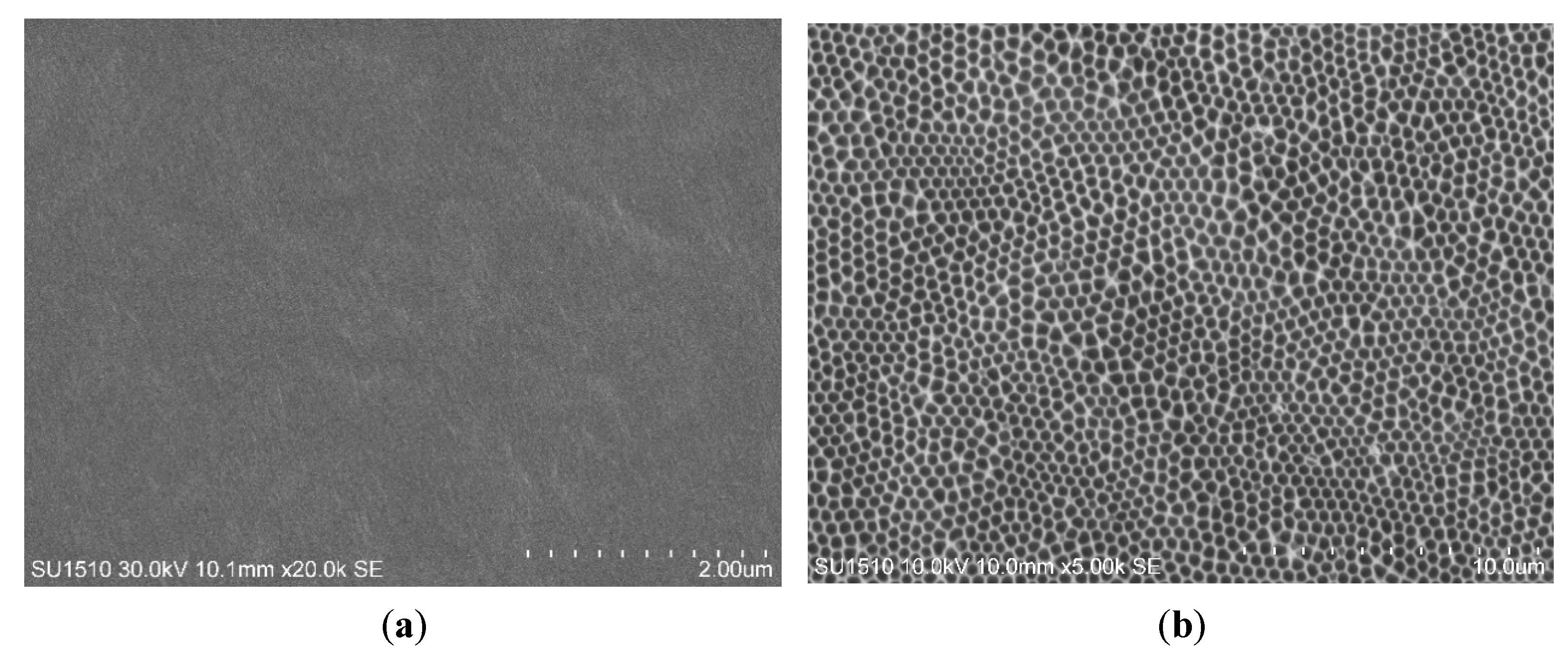
Metal-assisted chemical etching (MACE) is advantageous compared with conventional methodologies such as chemical vapor deposition (CVD), Thermal Evaporation (TE), laser ablation, electrochemical synthesis and electron beam lithography because of its moderate reaction conditions, convenient operation and short fabrication period for the synthetic process [
13,
14,
15]. The noble metal constituting a dense layer deposited on monocrystalline silicon as an etching catalyst used in MACE is a key factor in the anisotropic etching process. In this work, randomly distributed Ag films and ultra-thin Au films with ordered nanomesh arrays of appropriate thickness were deposited via chemical reaction and ion sputtering, respectively. Noble metal particles in a HF-containing solution tend to form ordered and disordered porous structures due to metal-induced localized etching of the surface of a silicon wafer [
16,
17]. Owing to the addition of organic or inorganic chemical reagents to the experimental process, the catalysis of noble metals and stress generated during etching, there is inevitable damage to the integrity of the crystal lattice and the formation of contaminated membrane layers, thus inducing lattice distortion and changing the simple harmonic vibration of the lattice. Structural defects, surface impurities and non-dense sensitive elements for SiNWs strongly influence the physical properties of materials, further affecting the external photoelectric effect. Above all, the quantum confinement effect caused by etching bulk silicon into nanowires induced modified physical properties, as revealed by the presence of a frequency shift, broadening and asymmetry in the corresponding Raman spectra [
18]. In this article, the effects of various mechanisms on the observed Raman scattering peak’s deviation from symmetry, redshift and broadening are analyzed. Therefore, we investigated the deviation of SiNWs from the monocrystalline silicon scattering peak by changing the diameter of the nanowire columns through thermal expansion to further analyze the effect of high-temperature annealing on Raman characteristics. Raman spectra also serve as a tool for detecting elementary excitations, such as phonon and electron behavior, in semiconductors. The information provided by Raman spectra can assist in improving the external physical effects of solid materials. Moreover, the deeper probing of the morphological characteristics of SiNWs is particularly important not only to improve the sensitivity to incident light and extend the detection band of nanomaterials but also to explore the potential applications of photovoltaic devices and photoelectric sensors with silicon microelectronics so that they may become reality.
4. Discussion
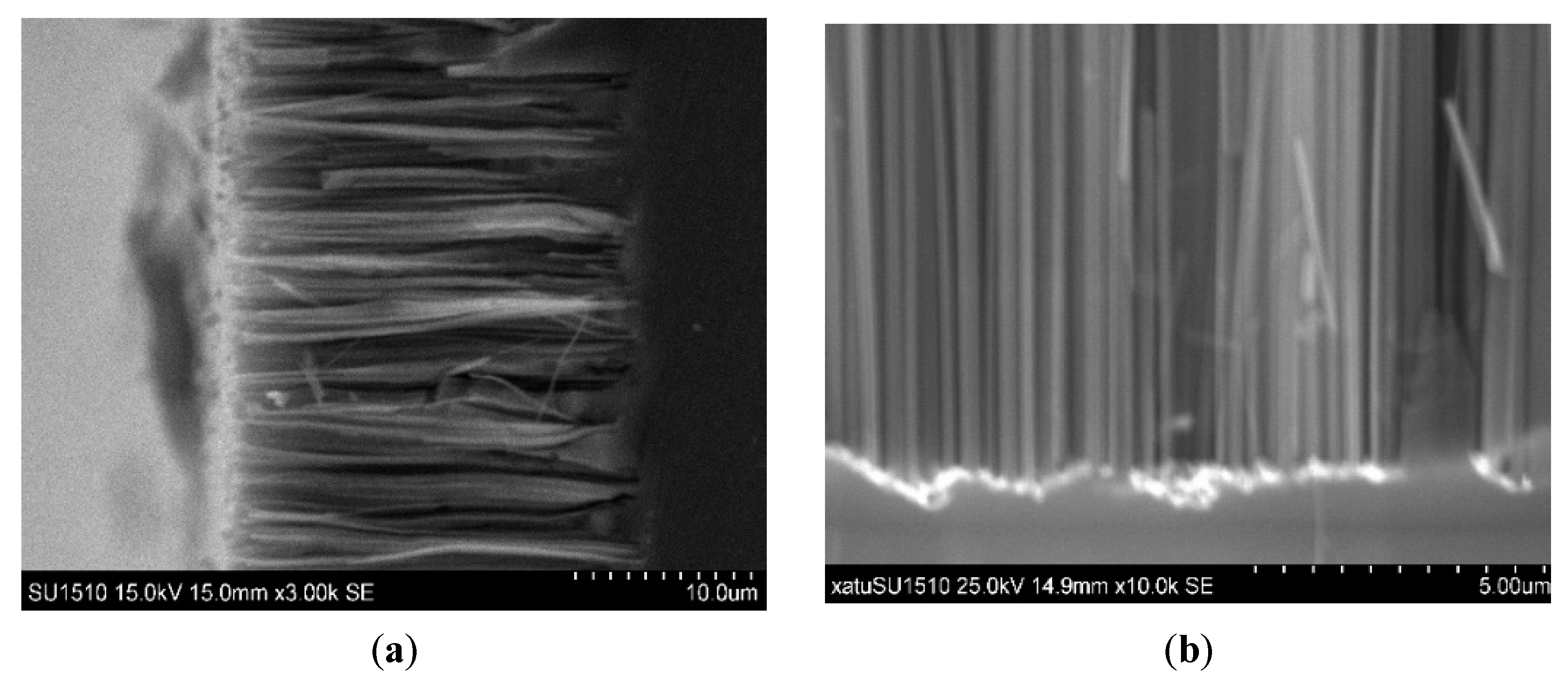
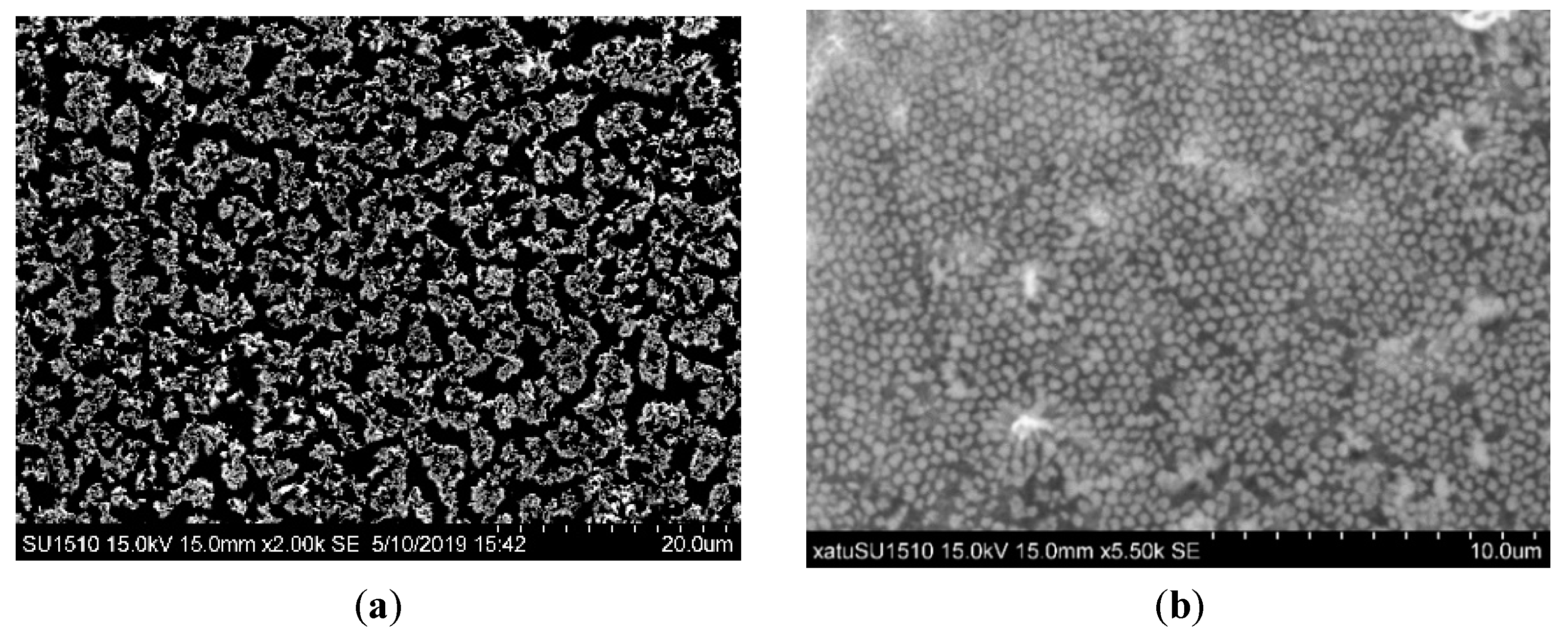
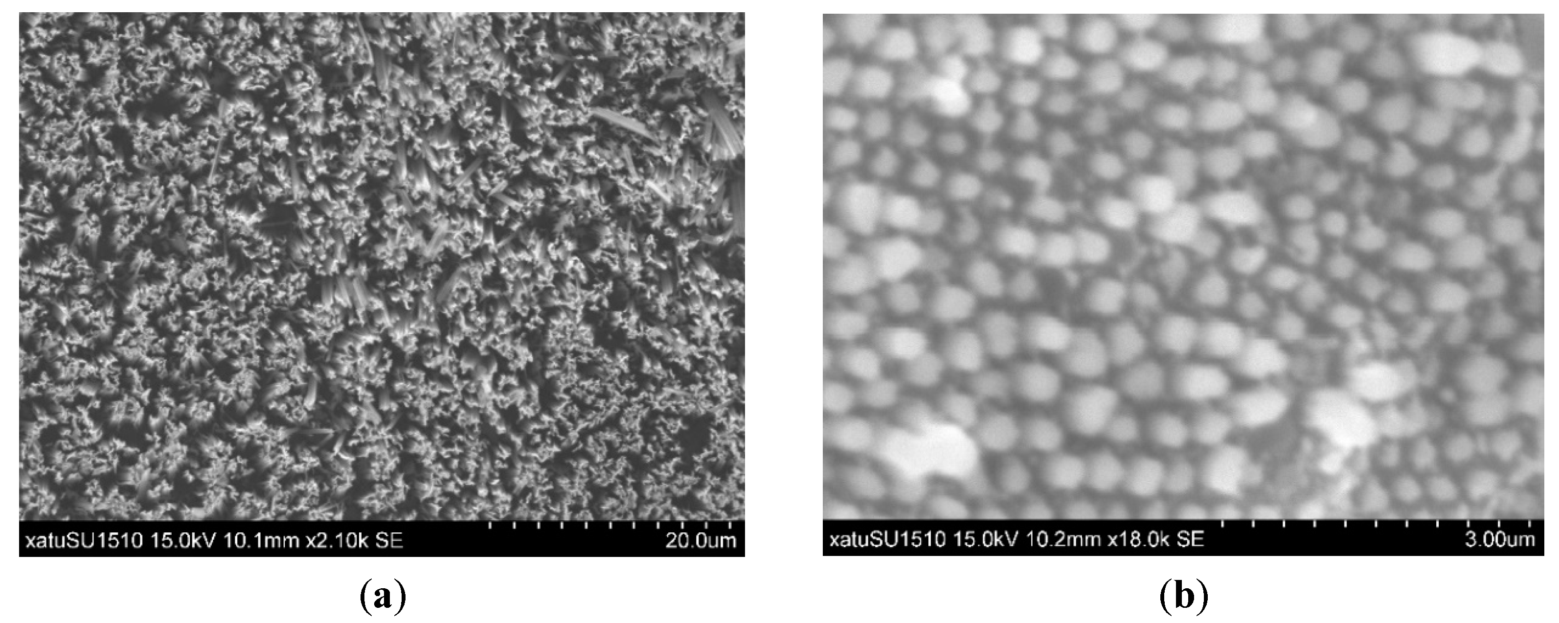
Figure 3 and
Figure 4 show the microstructural comparison of SiNWs before and after annealing. Before annealing, the surface of the SiNWs fabricated with randomly distributed Ag films presents a dendritic microstructure with high porosity, and the surface of the substrate coated with the spatially ordered mesh Au films form numerous tiny nanowire columns whose structures are consistent with the morphology of the Au nanomesh. After annealing, both of the surficial structures of the two morphologically different arrays are thermally expanded. The nanowires of disordered arrays are clustered, causing an increase in the interfacial area. Meanwhile, the adjacent wire spacing of the ordered arrays becomes denser, presenting a more uniform distribution in the volume of the etching layer.
Due to the internal carrier transport mechanism and external experimental conditions, it is inevitable that intrinsic and extrinsic lattice defects destroy the crystal symmetry in the constituting areas, and stress produced by noble metal catalysts in the etching process changes the phonon vibration frequency. We found that a large number of bubbles generated during the chemical etching process produce huge stress on the surfaces of silicon columns, which causes defects and microcracks in the relatively fragile grain boundaries. Simultaneously, calculations showed that more vacancies exist on the grain boundary in the disordered array than in the ordered array, and they are generated in the process of nanowires being pressed from blocks into particles. The first experiment revealed that the high surface activity of the Ag film produces excess positive holes, which diffuse to the top or side wall of silicon wires [
17], resulting in secondary etching for disordered arrays. However, the interaction of HF with AgNO
3 during the silver-plating process can lead to the formation of nitric acid, which, together with HF, will etch silicon. When etching monocrystalline Si wafers, vacancies are formed that will merge into the pores. Naturally, places that are covered with metal will not be as etched as places free of coating. During the preparation of the ordered array, the AAO membranes need to be removed as sacrificial layers. It is quite possible that there is an associated increase in the unintentional deposition of residual aluminum oxide on arrays due to the NaOH solution not completely dissolving AAO, which would affect the probability of carrier recombination.
Higher activation energy generated by the initial high-temperature annealing is provided to the deviated silicon atoms. This makes it possible to promote the diffusion of oxygen atoms into the material, accelerating oxidation. The oxide formation process mainly includes the combination of O-containing bonds and suspended bonds after H removal from the surface of nanowires. The small amount of oxide and grains with different shapes appearing on the surface of the array could be observed after annealing. It is conjectured that there exists an amorphous and polycrystalline layer containing many silicon nanoclusters embedded in oxidized silicon on the surface [
25]. During the high-temperature heating process, the adsorbed silicon atoms and silica particles receive enough energy to diffuse into the amorphous and polycrystalline layers. Moreover, pores existing on the top and side of silicon nanowires could contract when heat is applied, or even disappear, indicating the formation of compact films. It should be noted that the structural evolution of SiNWs is dependent on the annealing time and temperature. The homogeneity of the microstructured arrays can be obtained by setting moderate annealing conditions.
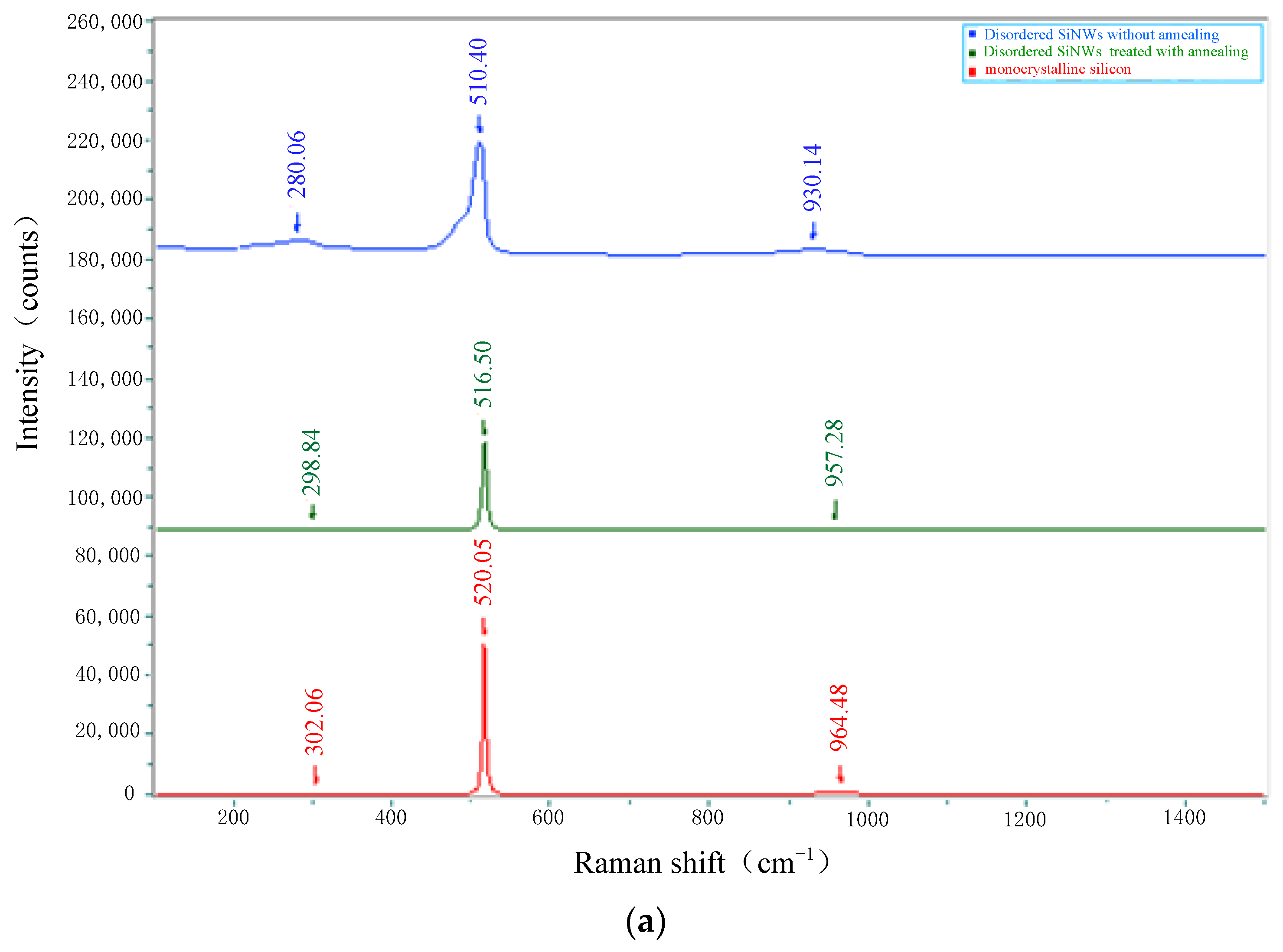
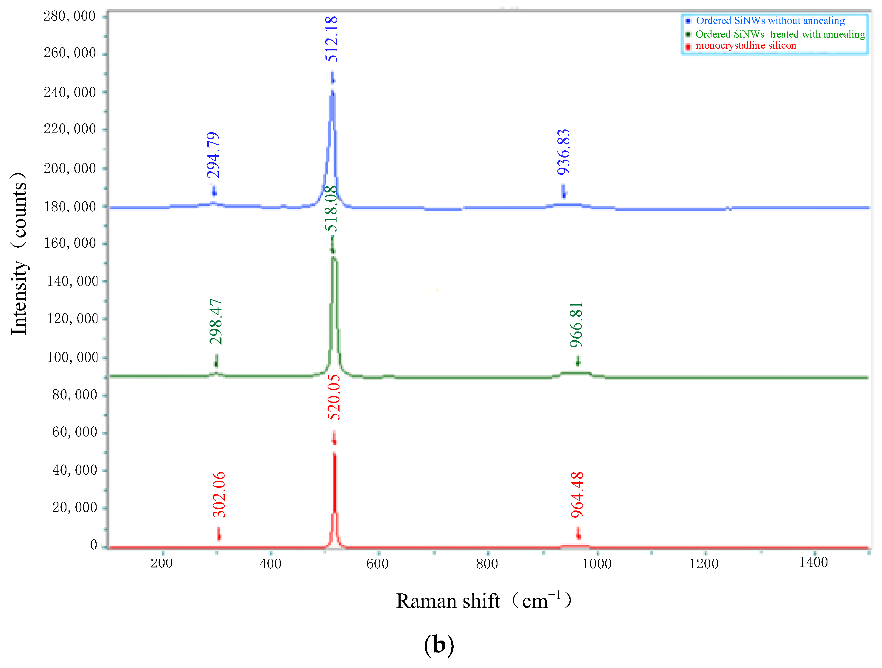
SiNWs samples with different structures before and after annealing used for the Raman scattering study were synthesized using various types of noble metal film catalysts with different morphologies. As shown in
Figure 5, we can see the related assignment of scattering peaks in the Raman spectra of prepared samples. The main strong sharp peak of monocrystalline silicon is measured at 520.05 cm
−1 with a symmetric lineshape, which derives from first-order optical phonon scattering with triple-degenerate Γ 25. In addition to the main peak with the highest intensity, there are two broad peaks with very weak intensity at 302.06 cm
−1 and 964.48 cm
−1, which are transverse optical biphonon peak (2TO) and transverse acoustic biphonon peak (2TA) scattering, respectively. The biphonon peak is caused by two consecutive single-phonon Raman scattering events, so the frequency shift of the biphonon spectrum should be the sum or difference of the single-phonon spectrum frequency shift [
26]. The scattering intensities measured in Raman spectra can lead to conclusions concerning microstructural parameters such as bonding, as well as deviations from the ideal crystalline structure [
27].
The characteristic values of the measured Raman bands can vary significantly depending upon which peak profile function is used in the fitting [
28]. After the comparison of the main peak fitting profile by Gaussian, Lorentzian and Gaussian–Lorentzian functional forms in LabSpec 6.3 software, the Gaussian fitting profile was used for the Raman spectra analysis of four test samples to realize the peak-splitting fitting calculation of superimposed peaks and obtain corresponding characteristic parameters, including the peak position, peak intensity, half-height width and peak area. The original spectral information is characterized by the feature parameters obtained from Gaussian peak fitting, and the fitting results are shown in
Figure 6 and
Figure 7.
In
Figure 5, the main peaks around 510.04 cm
−1 (disordered SiNWs without annealing), 516.5 cm
−1 (disordered SiNWs with annealing), 512.18 cm
−1 (ordered SiNWs without annealing) and 518.08 cm
−1 (ordered SiNWs with annealing) move toward lower frequencies. Because of first-order optical phonon scattering, the representative Raman peak of monocrystalline silicon appears at 520 cm
−1. As shown in
Figure 4b, the diameter of the annealed nanowire columns is 0.3 µm; this value is then substituted into the following formula [
29,
30]:
where
d is the diameter of the nanowire columns,
B is a constant related to the material,
ωb is the crystalline TO peak location of monocrystalline silicon, and
ωn is the TO peak location for SiNWs.
ωb −
ωn is the deviation of the measured SiNWs peak location from the monocrystalline silicon peak at 520.05 cm
−1. We can deduce
B = 4496 cm
−1 nm
2 from the integrated Raman scattering peak intensity at 520.05 cm
−1 and at around 518.08 cm
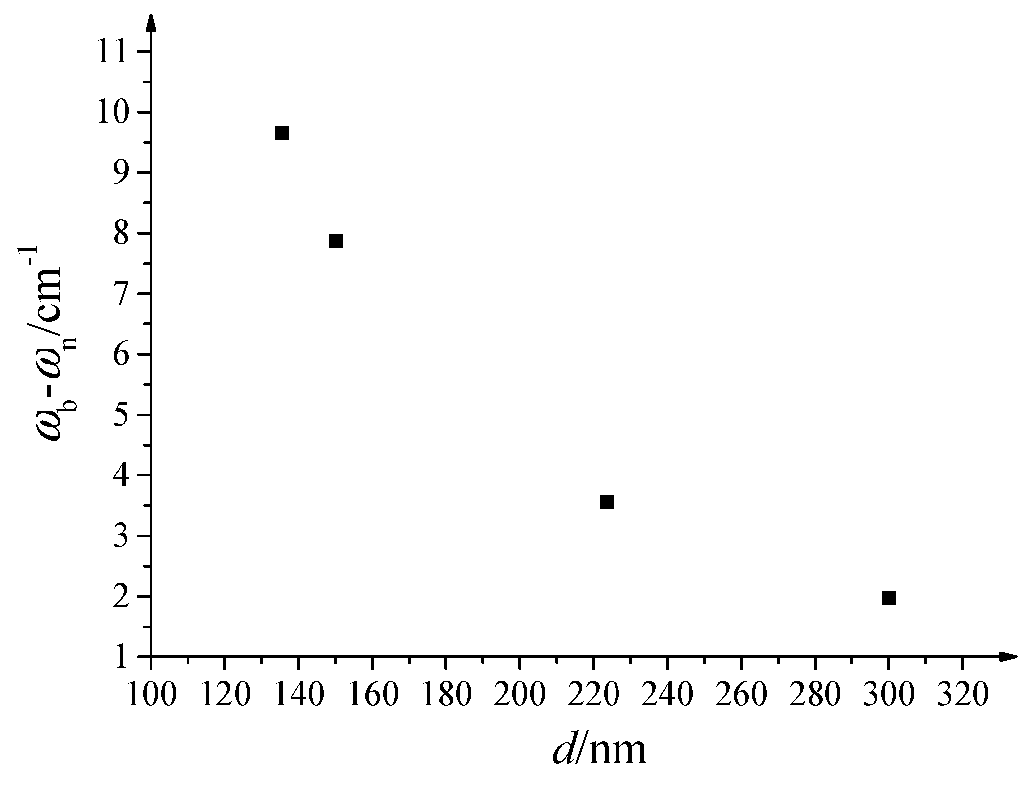
−1 with ordered SiNWs after annealing. We also calculated the estimated value of the diameter of disordered nanowire columns before and after annealing to be 135.553 nm and 223.49 nm, respectively. According to the calculation results, the relationship curve between
ωb −
ωn and the nanowire columns
d is plotted.
As shown in
Figure 8, the deviation of two samples with thermal expansion from the monocrystalline silicon peak at 520.05 cm
−1 is smaller compared with arrays without annealing. This can be attributed to the progressive decrease in the lattice constant as a function of the nanowire column size, which has an impact on the phonon vibration frequency. The problem associated with the redshift of scattering peaks becomes worse as the phonon vibration frequency increases. According to measurements of ordered arrays, the redshift characteristics arise as the diameter of the nanowire columns increases. For each 150 nm increase in diameter, the deviation decreases by approximately 5.9 cm
−1.
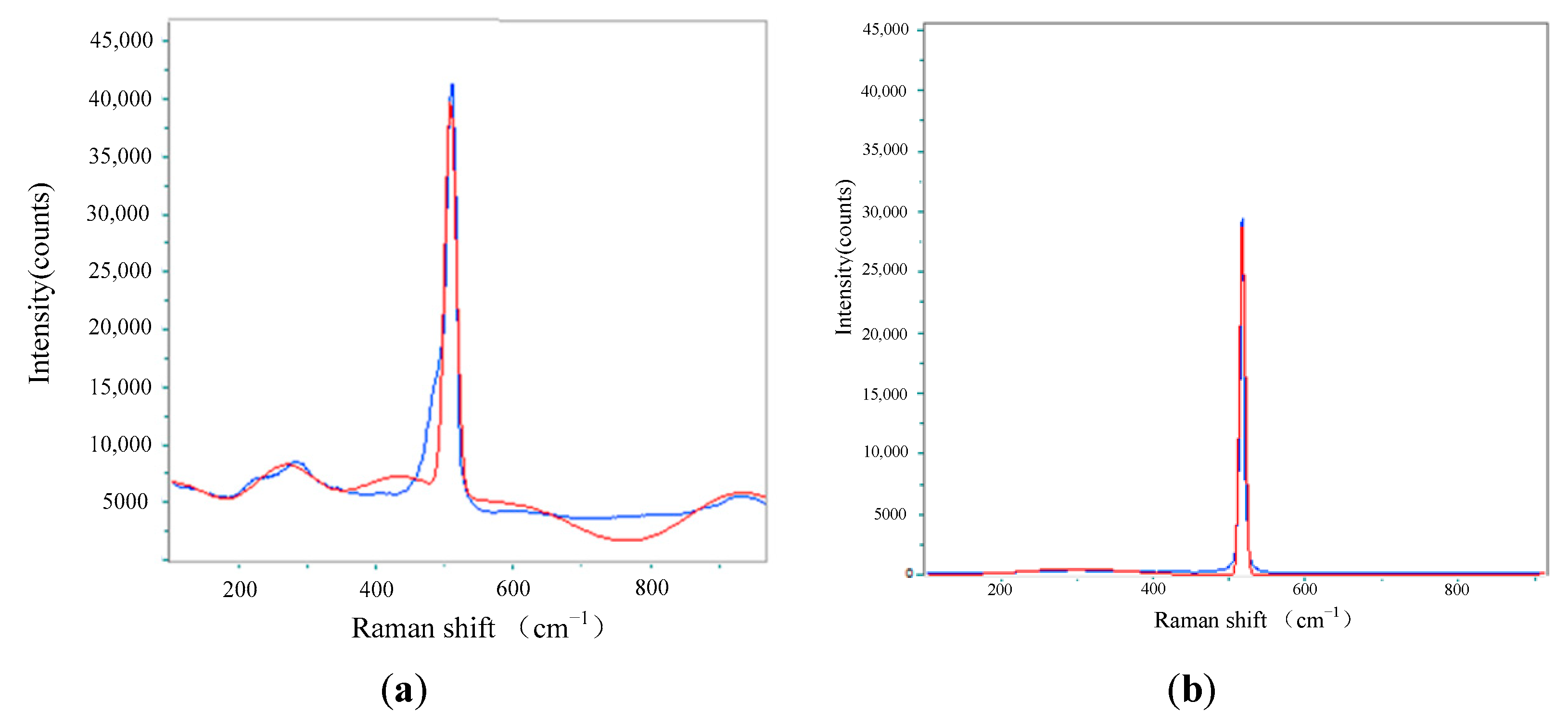
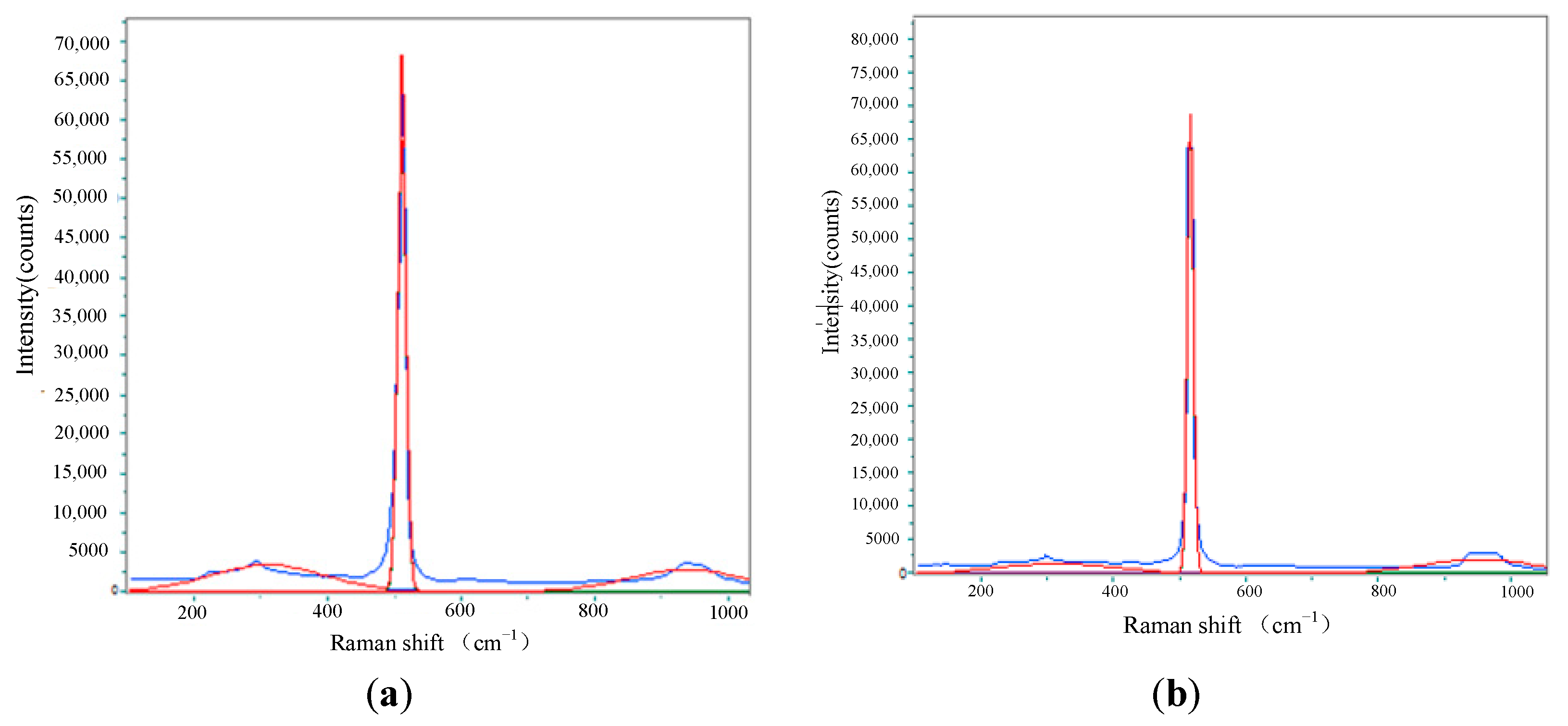
A preliminary test revealed that the redshift and broadening of the main peak of the ordered array are weaker than those of the disordered array. Besides the existence of an amorphous and polycrystalline layer caused by extremely tiny nanowires in the disordered array, this would have been affected by the morphology and type of the noble metal catalyst causing ambient pressure in the synthesis process of silicon wires. The interface between the silicon nanowires and the substrate generates external stress induced by the space constraints of noble metal films, as well as the residual stress caused by the capillary effect of liquid volatilization. The existence of external stress changes the bond length between internal molecules, thus changing the vibration frequency of the lattice and causing a change in the spectral lineshape. During the etching process, the external stress produced by the catalytic etching of the Ag film is possibly higher than that of the spatially ordered mesh Au film. So, the observed redshift and asymmetric broadening of spectral lines for disordered arrays are much more pronounced than those of ordered arrays. The primary reason for this phenomenon may be related to the electrical conductivity of noble metals. The conductivity of Au as a catalyst is stronger than that of Ag. The enhancement of metal conductivity enables electrons to be transmitted as fast as possible to the interface between the metal film and the solution. Meanwhile, protons do not have enough time to diffuse to the interface between the metal film and the silicon wafer, thus forming a concentration gradient, which means that the metal particles are in a larger self-built electric field, accelerating the etching rate [
31,
32]. The higher transfer rate of carriers means that the process of carrier relaxation, recombination and deep-level defect state binding in the system can be effectively avoided. Previous studies reported that the etching rate of a silicon wafer is very sensitive to local strain. Assuming that nanowires continue to form after the initial etching, exposed surfaces with tensile strain need to be stabilized by lattice shrinkage. Then, the residual strain effect is very significant in extreme cases, which possibly leads to nonlinear elastic deformation, superelasticity and even lattice phase transitions, resulting in changes in the measured Raman spectral curve.
As depicted in
Figure 5, the redshifts of the scattering peaks of the two morphologically different arrays after annealing are smaller than those before annealing, with stronger symmetry and weaker peak broadening. The silicon atoms deviating from the lattice position receive enough energy to snap back to the vacancies at lattice node positions. The small defect clusters and lattice stress are gradually restored as heat is applied. The roughness of the side wall of the silicon wires could cause phonon scattering. The crystal defect causes the propagation of phonon waves in materials to be attenuated, leading to the relaxation of the momentum conservation rule. That is, some
k ≠ 0 phonons are also excited. This manifests as the asymmetry and broadening of the Raman spectral shape, thus causing the change in the phonon spectrum.
where
ω is the phonon frequency;
k is the wave vector of the phonon;
L is the correlation length, associated with the density of defects in crystals; and Γ
0 is the half-peak width of the Raman spectra for the complete crystal. Considering the phonon dispersion relation near the center of the Brillouin zone,
The relationship between the redshift of the Raman peak, the correlation length
L and the half-peak width Γ
0 can be calculated by using Formulas (2) and (3). Beyond that, another possibility is that SiNWs lacking a passivation layer possess extremely high effective surface recombination velocity. It is speculated that some areas of ordered SiNWs could be effectively passivated by the residual AAO, which exhibited a promising effective carrier lifetime upon post-deposition annealing. Van Hoang Nguyen et al. [
33] demonstrated that the effective carrier lifetime of SiNWs drastically increased upon post-deposition annealing under thermal treatment at about 650 °C. This is possibly due to the carriers easily diffusing because of a reduction in defects at the bottom of the SiNWs. S. Ben Dkhil et al. [
34] concluded that thermal annealing gave rise to a reduction in the charge separation efficiency and thus in their transfer at the interface between the substrate and silicon nanowires.
The finite linewidth of SiNWs gives rise to confined modes, causing asymmetry and an increase in the Raman scattering intensity compared with the red line in the low-frequency region of the longitudinal optical (LO) or transverse optical (TO) phonon peaks [
35]. As the crystallite is reduced to the nanoscale, the phonons with a wave vector participate in first-order Raman scattering. The wave-vector balance may be broken, resulting in the appearance of surface and interface vibration modes. Phonon scattering that is not limited to the center of the Brillouin zone of the Raman spectra can be taken into account [
27]. In
Figure 5, the full width at half maximum (FWHM) on the pre-maximum side is increased due to the quantum confinement effect, resulting in asymmetric broadening toward the lower-energy side of the main peak [
36]. It is clear that the FWHM of the main peak after annealing is much lower than that before annealing, as illustrated in
Table 1, indicating that annealing improves the compactness of the film, which is also consistent with the microstructure observed by high-resolution SEM in
Figure 4. In addition, the existence of the Fano interaction caused by heavily doped p-type silicon used in the experiment could induce an increased half-width in the post-maximum side [
18]. The amorphous silicon oxide layer formed on the silicon nanowire surface after etching and the existence of structural defects in SiNWs can also strongly influence the change in the Raman scattering peak [
37].
In addition to the above factors, it is necessary to analyze the effects of other various mechanisms on the observed symmetry-forbidden mode of the Raman curve for a further understanding of the crystal structures of the samples. It is widely known that laser irradiation (incident light power exceeding several milliwatts) sparks the frequency redshift of scattering peaks for silicon wires. It is difficult to release the heating energy accumulated inside the silicon wires because of the small contact area with the substrate. Scientists are concerned about the thermal conductivity of silicon nanowire arrays. Al Hochbaum et al. noted that [
38] SiNWs with diameters of about several tens of nanometers exhibit a 100-fold reduction in thermal conductivity compared with doped bulk silicon, even if both have the same Seebeck coefficient and electrical resistivity values. However, the dependence of the observed redshift of the main Raman mode on thermal conductivity is not as clear. G.S. Doerk et al. [
39] demonstrated that no changes in lattice anharmonicity occur in relation to the silicon nanowire size; thus, the observed effect is probably due to the poor control of the sample temperature during spectroscopic measurements.
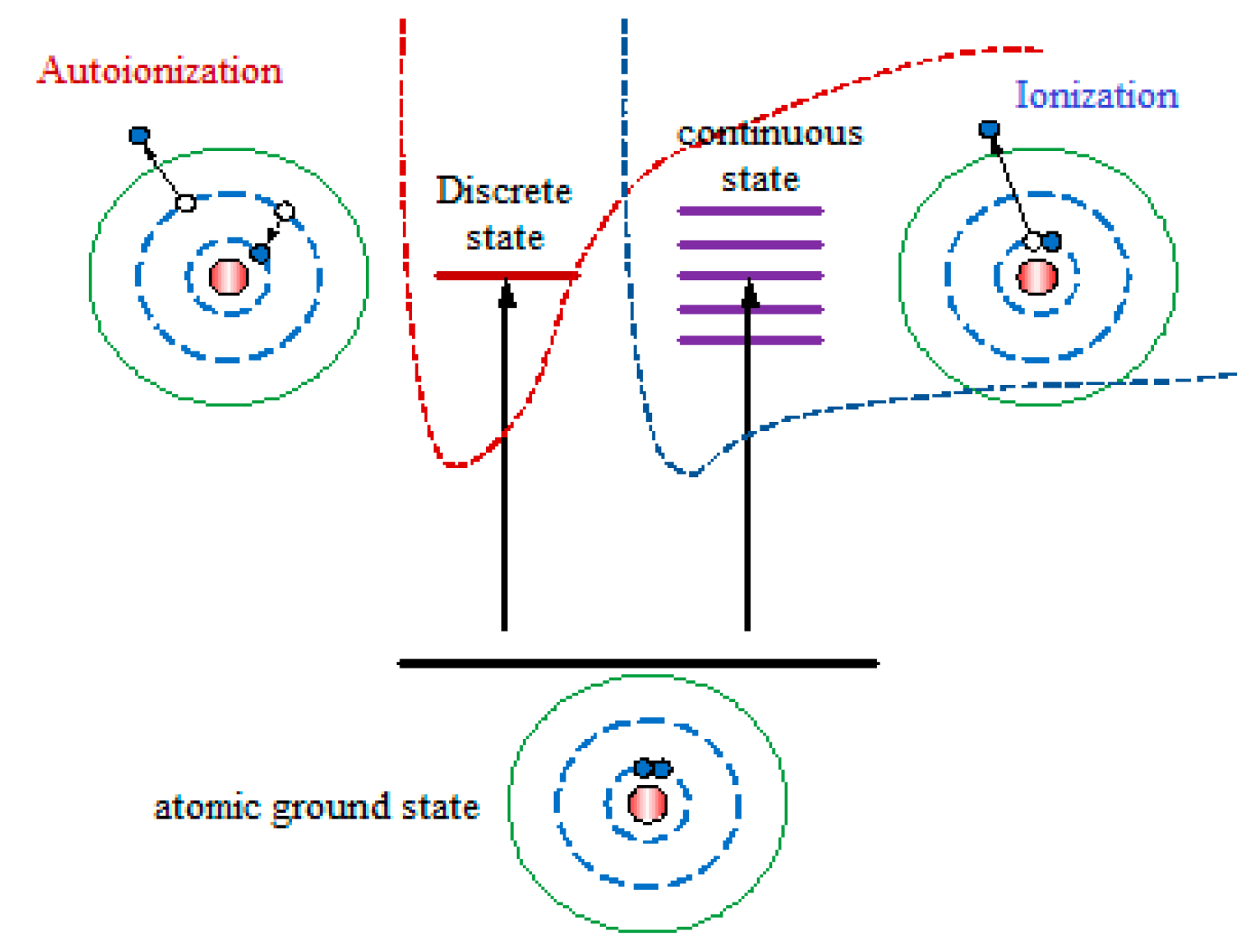
The asymmetry of the Raman peak lineshape is possibly also caused by Fano interaction in the material. The Auger effect indicates that electrons in the inner layer of the atom are stimulated by ionization to form vacancies. The electrons at higher energy levels that transition to these vacancies release energy, and other electrons in the outer layer of the atom absorb this energy and are stimulated. Stimulated electrons follow autoionization via the Auger effect and the direct ionization of inner electrons, as shown in
Figure 9.
The transition from the atomic ground state to the discrete state and from the atomic ground state to the continuum state are the two modes of atomic photoionization. The symmetrically distributed discrete state and the wide-spectrum continuous state are coupled to different paths, giving rise to asymmetric linear resonance through quantum interference. This observed asymmetric Breit–Wigner–Fano (BWF) lineshape of Raman spectra satisfies the following formula [
40]:
where s = (
ωs −
ωG)/Γ,
ωs is the Raman shift,
ωG is the spectral peak position and Γ is the spectral width. 1/
qBWF is the asymmetric factor;
I0 is the maximum intensity of the spectra. The above formula contains three terms: the constant continuum spectrum, the discrete Lorentzian spectrum and the interference effect between the two spectra. The asymmetric factor affecting the spectrum for SiNWs accounts for the various transition probabilities of internal electrons. First of all, the asymmetric lineshape could have occurred via the transition of free electrons in the conduction band, releasing low energy, owing to the energy reduction at the bottom of the conduction band caused by long-wave optical phonons. The overlap between the electronic continuum and discrete states causes interference effects, and Fano interference arises [
41]. The possible explanation is that the interference between the electronic Raman spectra and the phonon spectra leads to a great change in the constructive/destructive interference near the phonon spectra, which brings about additional asymmetry in the phonon lineshape fitting to the BWF lineshape [
40].


