Abstract
Accurate measurement of elastic constants in thin films is still an important issue to understand the scale behavior of nanosized materials. In the present study, we introduced an advanced non-destructive method, picosecond ultrasonics (PU), for measuring the out-of-plane elastic modulus of thin chromium (Cr) films. The femtosecond light pulse is focused on the Cr film to excite the longitudinal acoustic phonons (LAP), which propagate along the thickness direction and repeat reflections inside the Cr film. Then, the propagation/distribution of LAP is detected by the time-delayed probe light pulse through the photoelastic effect. Therefore, we can determine the out-of-plane modulus by measuring the periodic pulse echoes or the breathing mode vibrations within the Cr film. For most Cr films, the determined modulus is smaller than the corresponding bulk value and decreases with the decreasing thickness, while for some Cr films, it closes and may exceed the bulk value. This work describes the thickness-dependent elasticity of thin Cr films and provides evidence of the stiffness enhancement in Cr films on the Si substrate. In addition, since LAP with central frequency up to 310 GHz is excited in Cr films on the SiO2 substrate, we also demonstrate the potential of Cr films as high-frequency photoacoustic transducers.
1. Introduction
Chromium (Cr) films are widely used in various engineering applications as an adhesive layer [1], thermal diffusion barrier [2], solar absorber [3], and plasmonic sensor [4]. It is generally known that the properties of thin films are different from those of bulk materials. Many scientists have studied the structural variation, morphological variation, optical constants, and electrical properties of Cr films using a series of testing techniques such as X-ray diffraction (XRD) [1,2,5], scanning electron microscope (SEM) [1,4], and atomic force microscopy (AFM) [3]. As we know, few studies about the elasticity of Cr films have been reported to date. Notably, Nilsson et al. [6] calculated Young’s modulus of thin chromium cantilevers based on its bending behavior obtained with AFM. However, the above measurement always involves ambiguous effects caused by the gripping condition or nanocrystalline structure of the cantilevers. An alternative route to measure the elastic modulus of thin films is picosecond ultrasonics (PU), an advanced non-destructive testing technique based on the ultrafast laser pump–probe method [7,8]. Different from XRD, SEM or AFM, PU is based on the time-resolved photoacoustic signals and provides a deeper acoustic penetration than the optical absorption depth.
Various metal films, including Al [9,10,11], Au [12,13], Pt [14,15,16], Ni [17,18], and Cr [18,19], have been proven suitable for PU to generate and detect longitudinal acoustic phonons (LAP), which travels and repeat reflections along the film’s thickness direction. Based on the film thickness and the measured round trip time of LAP, we can determine the sound velocity related to the out-of-plane elastic modulus [20]. Among the above metals, the Pt, Ni, and Cr [18] have strong electron–phonon coupling constants and their thermal diffusion is typically confined to the optical absorption depth, resulting in ultrashort pulses of LAP; therefore, such metals are considered candidates for high-frequency photoacoustic transducers. Previous studies have shown that Pt [15] and Ni [17] can generate LAP with central frequency up to hundreds of gigahertz (GHz). For thin metal films, the out-of-plane elastic modulus can also be determined by the breathing mode central frequency of non-propagating LAP trapped in the film [16,20].
In this work, we present a systematic study on the measurement of elastic constant in Cr nanofilms using a two-color femtosecond laser pump–probe method. Four groups of polycrystalline Cr films (<200 nm) are deposited onto Si and SiO2 substrates as experimental samples. By utilizing the femtosecond light pulses, we excite and detect the typical acoustics signals in thin Cr films, including the periodic pulse echoes [18] and the breathing mode vibrations. With the detected round-trip time or breathing mode frequency, we determine the out-of-plane elastic modulus of thin Cr films. We investigated the thickness dependence, the softening effect and stiffening behavior of elasticity in thin Cr films. We also demonstrated the potential of thin Cr films as high-frequency photoacoustic transducers.
2. Materials and Methods
2.1. Sample Preparation
To ensure the universality of our research results, we prepare polycrystalline Cr films synthesized using two different physical deposition techniques on two different substrates. The first two groups of Cr films with thicknesses of 20 to 200 nm were sputtered onto Si and SiO2 substrates using magnetron sputtering (MS). The base pressure was 7.5 × 10⁻⁷ Torr, the deposition chamber pressure was maintained at 1.5 × 10⁻² Torr of Ar, and the sputter power was set at 60 W. The sputter rate was about 2.0 Å/and we changed the film thickness by controlling the sputter time.
For Cr films sputtered at 100 s, the cross-section image using SEM (ZEISS Gemini SEM 500, Oberkochen, Germany) in Figure 1a shows the thickness is around 18.55 nm, and the film thickness fitted using an ellipsometer in Figure 1b (Eoptics Technology Co., Wuhan, China) is approx. 19.87 nm. Therefore, we estimated the thickness of Cr film sputtered at about 100 s is approximately 20 nm. In Figure 1c, we also show an AFM (Olympus LEXT 4100 OLS, SPM mode, Tokyo, Japan) image of the Cr film sputtered at 100 s on the Si substrate. From the AFM images, we find that the root means square (RMS) surface roughness values are 1.163, 1.209 and 1.960 for the 20, 30, and 50 nm Cr films sputtered on the Si substrate, respectively. We also took AFM images of the glass substrate and obtained the RMS roughness values of 1.118, 1.148, and 1.517 nm for the 20, 30, and 50 nm Cr films, respectively.
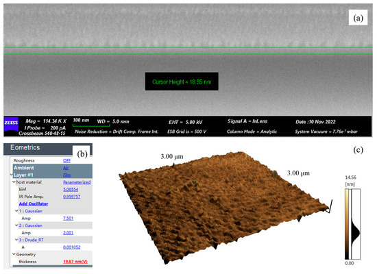
Figure 1.
(a) The cross-section SEM image, (b) the screen shot of Eometrics, an ellipsometer control software (version 3.5.5.0407), and (c) the AFM image of the Cr film sputtered at 100 s.
The second two groups of Cr films with a thickness of 8 to 200 nm were vaporized onto the Si and SiO2 substrates using an electron beam (EB) created by H-Chip Tech Group (Tianjin, China). Their chamber pressure was maintained at 5 × 10⁻⁶ Torr and the vaporization rate was about 0.5 Å/s.
2.2. Picosecond Ultrasonics Method
2.2.1. Experimental Setup
A typical time-resolved femtosecond laser pump−probe experiment setup was employed for the PU measurements of Cr films [19]. A mode-locked Ti:sapphire pulsed laser (Vitara-T, Coherent Inc., Santa Clara, CA, USA) was used to generate light pulses with a wavelength of 800 nm and duration of 20 fs at a repetition rate of 80 MHz. A two-color scheme was employed to enhance the signal-to-noise ratio of the experiment setup to ∼10−7. The laser beam was divided into the pump beam and the probe beam by a polarizing beam splitter and a half wave plate with an intensity ratio of 10:1. The pump beam was first focused onto a nonlinear BiB3O6 crystal to change the wavelength to 400 nm by the second harmonic generation, and then modulated at a reference frequency of 1 MHz using an electro optic modulator (Model 25A + 370-01, Conoptics Inc., Danbury, CT, USA) and a function generator (33509B, Keysight Technologies, Colorado Springs, CO, USA). The probe beam with a wavelength of 800 nm entered a variable optical delay path, a combination of two retroreflective mirrors mounted on a motorized linear stage (LTS300/M, Thorlabs Inc., Newton, NJ, USA). Both the probe beam and the pump beam were coaxially focused at vertical incidence to the sample using a cold mirror and a 10× objective lens. The diameter of the pump and probe beam is 90 and 30 µm (1/e2 diameter for intensity), respectively. The intensity of the reflected probe beam was converted to voltage signals and recorded by a Si amplified fixed-gain photodiode detector (PDA36A2, Thorlabs Inc., Newton, NJ, USA). Lock-in detection using a lock-in amplifier (SRS844, Stanford Research Systems, Sunnyvale, CA, USA) at the reference frequency of 1 MHz allows relative reflectivity change ∼ 10−7 to be extracted. The parameters of the lock-in detection were fixed in the measurement procedure. Therefore, the sampling speed was dependent on the movement of the motorized linear stage and configured to have a time step of 0.25 ps/pt in this study.
2.2.2. Measurement Theory
In the PU measurements discussed below, the metal film in the sample is used as a photoacoustic transducer to generate and detect high frequency LAP in the femtosecond pump–probe experiment. Once the pump beam enters the metal film, the electrons in the optical absorption depth are excited to higher states by the photons. Then, the hot electrons will diffuse into the metal film interior and heat the lattices through the electron–phonon coupling. The final spatial profile of the LAP is determined by the depth of heated region (that is, thermal diffusion). For metals with weak electron–phonon coupling such as Au [12,13] or Al [9,10,11,21], the depth of thermal diffusion can be up to ~100 nm and the corresponding frequency of LAP is ~10 GHz. In the case of metals with strong electron–phonon coupling, the depth of thermal diffusion is relatively small, usually in the order of the optical absorption depth. For example, for a vertical incident pump beam at 415 nm, the depth of thermal diffusion in sputtered Cr films is about 15 nm [18]. In addition, when the metal film is thin enough, the depth of thermal diffusion is also limited by the film thickness of thin film. Therefore, the relatively short diffusion depths allow the excitation of much higher-frequency LAP > 100 GHz.
For the PU measurement, the reflected probe beam monitors the relative reflectivity change of the metal film transducer, including the LAP disturbance as acoustic signals and temperature change as thermal signals. For the analysis of the measured acoustic signals from the Cr films, it is important to separate the slow decaying thermal signal caused by the thermal diffusion. In this study, we removed the thermal signals by subtracting an exponentially decaying function from the data [22]. By solving Maxwell’s equations inside the metal film [7], the acoustic signals in the reflectivity change can be expressed as
where
In Equations (1)−(4), the was defined as “sensitivity function”, which determines how the LAP at different depths below the film surface contributes to the reflectivity change , is the wavelength of probe beam, and are the real and imaginary components of the complex refractive index of film, is the only nonzero component of the elastic strain tensor, is the optical absorption depth, and is the arbitrary phase in the range of 0 to π/2 [7].
2.2.3. Typical Acoustic Signals
Figure 2 shows the two kinds of typical acoustic signals and corresponding Fourier spectra of the first two groups of Cr films sputtered on the Si and SiO2 substrates with MS. When the thickness of Cr films exceeds 60 nm, LAP are excited at a limited depth determined by thermal and nonequilibrium electron diffusion [18], propagate along the thickness direction, and repeat reflections between the film and the substrate surfaces. Considering that both the pump and probe beam diameters are much larger than the film thickness, a quasi-one-dimensional assumption was adopted for the propagation and reflection of LAP [7]. Therefore, several equally spaced echoes were observed in the acoustic signals of 100 nm Cr film (Figure 2a). Using the round-trip time between the successive echoes, the sound velocity can be expressed as
where d is the film thickness.
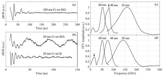
Figure 2.
Typical acoustic signals obtained from (a) the 100 nm vaporized Cr film and (b) 20 nm sputtered Cr films. The Fourier spectra of thin sputtered Cr films on (c) Si substrate and (d) SiO2 substrate. Vertical arrows indicate the Brillouin oscillations from the substrates.
For thin Cr films (d ≤ 60 nm), we observe a rapidly decaying oscillation that appears just after the excitation, followed by another oscillation with different frequencies on different substrates (Figure 2b). The latter oscillation, typically identified as the Brillouin oscillation, is caused by the interference between the probe beam reflected at the substrate surface and diffracted by the propagating LAP in the substrate [23,24]. For materials that are transparent at the probe beam wavelength, the PU is originally referred to as picosecond acoustic interferometry and currently called the time–domain Brillouin scattering [23,24]. The corresponding Brillouin frequency is given by
At vertical incidence, where n, vs and are the refractive index of the substrate, the sound velocity of the substrate, and the wavelength of the probe light. Taking standard handbook values, the calculated Brillouin oscillation frequencies are 79 GHz and 22 GHz for Si and SiO2 substrates, respectively. The values agree with the arrow indicated in Figure 2c,d. In addition, the first peak around 10 GHz in Figure 2c is a false peak generated by the Fourier transform of signals in limited sampling time. Once we extend the time length of signals to 100 ps or more, the false peak will disappear.
The former oscillation, considered breathing mode vibrations [19], is caused by the non-propagating LAP trapped in the film. The LAP was induced by the uniform optical excitation of the thin film. Since the acoustic impedance of the film is larger than that of the substrate, the sound velocity is given by
where d and f are the film thickness and breathing mode frequency [16,22]. It has been shown that thin Cr films on the Si substrate in Figure 2c have broader peaks than the SiO2 substrate in Figure 2d, which is in accordance with the fact that the acoustic impedance mismatch of Cr-Si is larger than that of Cr-SiO2.
As stated above, we showed the two typical acoustic signals: periodic pulse echoes in Figure 2a and breathing mode vibrations in Figure 2b, and we obtained the sound velocity by the round trip time or breathing mode frequency. Using the mass density ρ and the determined sound velocity v, we can calculate the out-of-plane elastic modulus as follows:
For the present calculation, we set the bulk value of ~7.2 g/cm3 [25] for the density ρ of Cr films.
3. Results
Figure 3 shows different breathing mode vibrations, corresponding Fourier spectra, and out-of-plane elastic modulus C33 of Cr films vaporized on the SiO2 substrate by EB. As shown in Figure 3a,b, the frequency of breathing mode is increased with the decrease of the film thickness. For the 8 nm Cr film, we generated LAP with the central frequency up to 310 GHz, whereas no breathing mode vibrations signals found in thinner Cr films on the SiO2 substrate. Additionally, there are no photoacoustic signals in PU measurements of the vaporized Cr films on the Si substrate. Therefore, the result of vaporized Cr films on the Si substrate are not shown in Figure 3 and reported in this study.
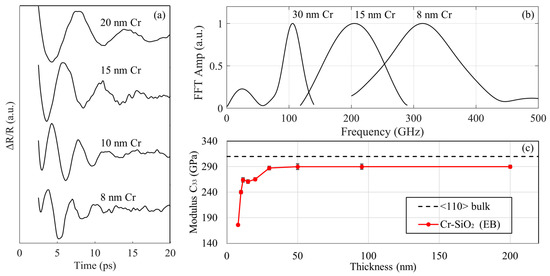
Figure 3.
(a): The breathing mode vibrations, (b): the corresponding Fourier spectra, and (c): the out-of-plane elastic modulus C33 of Cr films vaporized on the SiO2 substrate by EB. The broken line denotes the modulus of the monocrystal bulk Cr along the <110> direction.
Figure 3c show that the out-of-plane elastic modulus C33 decrease with the decrease of the film thickness due to the thin-film softening effect, which has been reported in thin films of Au [12], Ni [17], and Ru [22]. For comparison, we calculated the elastic modulus along the <110> directions using the known Cij of monocrystal Cr by [26]. It has been reported that polycrystalline films made from fcc materials, like Cr [5], Pt [15] and Fe [16], have the preferred <110> crystallographic direction in the film thickness direction. Therefore, the is the ideal C33 of bulk Cr, and the maximum value for C33.
Figure 4 shows the out-of-plane elastic modulus C33 of the first two groups of Cr films deposited sputtered on the Si substrate and SiO2 substrates by MS. The trend like the thin-film softening effect in Figure 3c is observed in both Figure 4a,b that C33 of Cr films first maintain a stable value in the range of 80 to 200 nm, and then decrease with the decrease of the film thickness in the range of 50 to 80 nm, regardless of the substrate materials. However, when the film thickness is smaller than 50 nm, C33 of Cr films on the Si substrate in Figure 4a start to increase with the decrease of the film thickness, finally close and may exceeds the maximum . In contrast, C33 of Cr films on the SiO2 substrate still smaller than the ideal value of bulk Cr in Figure 4b.
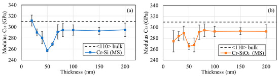
Figure 4.
The out-of-plane elastic modulus C33 of Cr films sputtered on (a) the Si substrate and (b) the SiO2 substrate by MS. The broken line denotes the modulus of the monocrystal bulk Cr along the <110> direction.
4. Discussion
As a transition metal with strong electron–phonon coupling, it has been investigated in 190 nm Cr film [18] that the relatively short diffusion depth governed by both thermal and nonequilibrium electron diffusion allows the excitation of high-frequency LAP; therefore, such Cr has potential as an ultrasonics transducer at frequencies >100 GHz. As shown in Figure 2a,b, the thinner thickness of Cr films results in the shorter diffusion depth and allows the excitation of higher-frequency LAP. It can be seen in Figure 1 and Figure 2b,c that the corresponding central frequency ranges from 50 to 310 GHz. The 20 nm and 10 nm Al films have been used as the photoacoustic transducer to generate 50 GHz and 100 GHz LAP [11], respectively. Here, our results in Figure 3b demonstrate that Cr films vaporized using EB can generate higher-frequency LAP at a thickness similar to that of Al films. This provides an alternative choice of the photoacoustic transducer for studying the attenuation of LAP in the GHz regime.
Based on periodic pulse echoes in Figure 2a and breathing mode vibrations in Figure 2b, we obtained the thickness dependence of C33 of three groups of Cr films in Figure 3c and Figure 4a,b. It can be seen that most Cr films have a stable elasticity with values slightly smaller than the corresponding bulk value, which is consistent with the fact that thin films are softer than bulk materials. The softening trend of C33 is observed for vaporized Cr films ranging from 8 to 50 nm in Figure 3c and sputtered Cr films ranging from 50 to 80 nm in Figure 4a,b. Since there are many mechanisms for the softening effect, including defects such as incohesive bonds, oriented nano-cracks, precipitates at grain boundaries, and interfacial strain, etc., it is difficult to identify the specific cause of the softening Cr films. The comparison between Figure 4a,b helps us to exclude the influence of substrate material on the softening trend of sputtered Cr film ranging from 50 to 200 nm.
Nilsson et al. reported Young’s modulus of 50, 68, and 83 nm thick Cr cantilevers measured using an AFM in contact mode [6]. Compared with our results, the reported Young’s modulus of Cr cantilevers is much smaller, which may be attributed to the decrease in Young’s modulus to the gripping condition [20], materials properties of the cantilevers, or the invalid equation for such nanosized beams, according to the authors of [6]. Nevertheless, similar softening trends were both observed in the sputtered Cr films in Figure 4a,b and Cr cantilevers [6] ranging from 50 to 83 nm. These trends may be helpful for us to further investigate the softening law of nano-sized chromium. Therefore, we can conclude that PU, as a non-destructive testing technique of elastic parameters, is competitive with the mechanical method using Cr cantilevers with an AFM in contact mode.
In addition, compared with sputtered Cr films on the SiO2 substrate in Figure 4b, we observe the stiffness enhancement in Figure 4a, as the Cr film on the Si substrate gradually stiffens with decreasing thickness ranging from 20 to 50 nm, and the increasing C33 finally may exceed its maximum value at 20 nm thickness. The stiffness enhancement in thin films on the Si substrate is rarely reported, which is attributed to strain-induced changes in third-order elasticity in thin Pt films [15]. The previous study of Ogi, H et al. [16] also reported the influence of substrate materials on the elasticity of thin Pt films. Comparing the Si and glass substrates, Ogi, H. et al. reported that the huge intrinsic stress inside the thin film and the low strength of the SiO2 substrate may cause the local failure and softer elasticity of thin films on the SiO2 substrate. This comparison is in accordance with our results in Figure 4a,b.
As discussed above, the out-of-plane elastic modulus of Cr films is affected by the film thickness, the deposition technique, and the substrate material. For the sputtered Cr films with a sputtering time of less than 100 s, there is no typical photoacoustic signal in PU measurements. To date, we attribute it to the existence of an island microstructure instead of a continuous structure in thinner sputtered Cr films. Further investigation of the effect of a microstructure on the generation of LAP should be considered.
5. Conclusions
In conclusion, we demonstrated the potential of Cr nanofilms as high-frequency photoacoustic transducers and systematically studied the thickness dependence of their out-of-plane elastic modulus C33 by PU measurements. The LAP with central frequency that ranges from 50 to 310 GHz are excited and detected in vaporized and sputtered Cr films with different thicknesses. The elastic modulus is smaller than the monocrystal Cr for most samples; however, it is may exceed the maxima of bulk value at the 20 nm sputtered Cr film on the Si substrate. This work offers guidance for Cr nanofilms as GHz photoacoustic transducers in the laser ultrasonics application and the design of film–substrate structures in nanomechanical devices.
Author Contributions
Conceptualization, X.T.; resources, data curation and investigation, X.T., J.L. and J.Y.; funding acquisition, project administration and supervision, L.L., Z.W. and S.W.; writing—original draft, X.T.; writing—review and editing, X.T., Z.W. and C.L. All authors have read and agreed to the published version of the manuscript.
Funding
This research was funded by the National Natural Science Foundation of China, grant number 12172251 and 12041201.
Institutional Review Board Statement
Not applicable.
Informed Consent Statement
Not applicable.
Data Availability Statement
Not applicable.
Conflicts of Interest
The authors declare no conflict of interest.
References
- Balu, R.; Raju, A.R.; Lakshminarayanan, V.; Mohan, S. Investigations on the influence of process parameters on the structural evolution of ion beam sputter deposited chromium thin films. Mater. Sci. Eng. B 2005, 123, 7–12. [Google Scholar] [CrossRef]
- Ezer, Y.; Härkönen, J.; Sokolov, V.; Saarilahti, J.; Kaitila, J.; Kuivalainen, P. Diffusion barrier performance of thin Cr films in the Cu/Cr/Si structure. Mater. Res. Bull. 1998, 33, 1331–1337. [Google Scholar] [CrossRef]
- Wang, Z.Y.; Hu, E.T.; Cai, Q.Y.; Wang, J.; Wei, W. Accurate Design of Solar Selective Absorber Based on Measured Optical Constants of Nano-thin Cr Film. Coatings 2021, 10, 938. [Google Scholar] [CrossRef]
- Msa, B.; Ss, A.; Mm, C.; Smid, E.; Wo, A.; Aa, B. Fabrication and Characterization of Au/Cr and Cr/Au Multilayered Plasmonic Nanofilms for Sensing Applications. J. Mater. Res. Technol. 2021, 11, 1868–1880. [Google Scholar]
- Sytchkova, A.; Belosludtsev, A.; Volosevičienė, L.; Juškėnas, R.; Simniškis, R. Optical, structural and electrical properties of sputtered ultrathin chromium films. Opt. Mater. 2021, 121, 111530. [Google Scholar] [CrossRef]
- Nilsson, S.; Borrise, X.; Montelius, L. Size effect on Young’s modulus of thin chromium cantilevers. Appl. Phys. Lett. 2004, 85, 3555–3557. [Google Scholar] [CrossRef]
- Thomsen, C.; Grahn, H.T.; Maris, H.J.; Tauc, J. Surface generation and detection of phonons by picosecond light pulses. Phys. Rev. B 1986, 34, 4129–4138. [Google Scholar] [CrossRef] [PubMed]
- Matsuda, O.; Larciprete, M.C.; Voti, R.L.; Wright, O.B. Fundamentals of picosecond laser ultrasonics. Ultrasonics 2015, 56, 3–20. [Google Scholar] [CrossRef]
- Lee, S.; Kim, Y.Y.; Cho, Y. A Comparative Study on the Elastic Characteristics of an Aluminum Thin-Film Using Laser Optical Measurement Techniques. Coatings 2017, 7, 143. [Google Scholar] [CrossRef]
- Grossmann, M.; Klingele, M.; Scheel, P.; Ristow, O.; Hettich, M.; He, C.; Waitz, R.; Schubert, M.; Bruchhausen, A.; Gusev, V.; et al. Femtosecond spectroscopy of acoustic frequency combs in the 100-GHz frequency range in Al/Si membranes. Phys. Rev. B 2013, 88, 205202. [Google Scholar] [CrossRef]
- Daly, B.C.; Kang, K.; Wang, Y.; Cahill, D.G. Picosecond ultrasonic measurements of attenuation of longitudinal acoustic phonons in silicon. Phys. Rev. B 2009, 80, 174112. [Google Scholar] [CrossRef]
- Wang, P.-J.; Shen, C.-C.; Chou, K.-Y.; Ho, M.-H.; Sheu, J.-K.; Sun, C.-K. Studying time-dependent contribution of hot-electron versus lattice-induced thermal-expansion response in ultra-thin Au-nanofilms. Appl. Phys. Lett. 2020, 117, 154101. [Google Scholar] [CrossRef]
- Yu, K.; Devkota, T.; Beane, G.; Wang, G.P.; Hartland, G.V. Brillouin Oscillations from Single Au Nanoplate Opto-Acoustic Transducers. ACS Nano 2017, 11, 8064–8071. [Google Scholar] [CrossRef] [PubMed]
- Yan, S.; Dong, C.; Miao, T.; Wang, W.; Ma, W.; Zhang, X.; Kohno, M.; Takata, Y. Long delay time study of thermal transport and thermal stress in thin Pt film-glass substrate system by time-domain thermoreflectance measurements. Appl. Therm. Eng. 2017, 111, 1433–1440. [Google Scholar] [CrossRef]
- Ogi, H.; Fujii, M.; Nakamura, N.; Yasui, T.; Hirao, M. Stiffened ultrathin Pt films confirmed by acoustic-phonon resonances. Phys. Rev. Lett. 2007, 98, 195503. [Google Scholar] [CrossRef] [PubMed]
- Ogi, H.; Fujii, M.; Nakamura, N.; Shagawa, T.; Hirao, M. Resonance acoustic-phonon spectroscopy for studying elasticity of ultrathin films. Appl. Phys. Lett. 2007, 90, 191906. [Google Scholar] [CrossRef]
- Chou, K.-Y.; Wu, C.-L.; Shen, C.-C.; Sheu, J.-K.; Sun, C.-K. Terahertz Photoacoustic Generation Using Ultrathin Nickel Nanofilms. J. Phys. Chem. C 2021, 125, 3134–3142. [Google Scholar] [CrossRef]
- Saito, T.; Matsuda, O.; Wright, O.B. Picosecond acoustic phonon pulse generation in nickel and chromium. Phys. Rev. B 2003, 67, 920–925. [Google Scholar] [CrossRef]
- Tu, X.; Zeng, Y.; Wang, S.; Li, L.; Li, C.; Wang, Z. Comprehensive Characterization of Thermal and Mechanical Properties in Thin Metal Film-Glass Substrate System by Ultrafast Laser Pump-Probe Method. Opt. Express 2022, 30, 46193–46208. [Google Scholar] [CrossRef] [PubMed]
- Ogi, H.; Nakamura, N.; Hirao, M. Picosecond ultrasound spectroscopy for studying elastic modulus of thin films: A review. Nondestruct. Test. Eval. 2011, 26, 267–280. [Google Scholar] [CrossRef]
- Lejman, M.; Shalagatskyi, V.; Kovalenko, O.; Pezeril, T.; Temnov, V.V.; Ruello, P. Ultrafast optical detection of coherent acoustic phonons emission driven by superdiffusive hot electrons. J. Opt. Soc. Am. B Opt. Phys. 2014, 31, 282–290. [Google Scholar] [CrossRef]
- de Haan, G.; van den Hooven, T.J.; Planken, P.C.M. Ultrafast laser-induced strain waves in thin ruthenium layers. Opt. Express 2021, 29, 32051–32067. [Google Scholar] [CrossRef] [PubMed]
- Gusev, V.; Lomonosov, A.M.; Ruello, P.; Ayouch, A.; Vaudel, G. Depth-profiling of elastic and optical inhomogeneities in transparent materials by picosecond ultrasonic interferometry: Theory. J. Appl. Phys. 2011, 110, 124908. [Google Scholar] [CrossRef]
- Gusev, V.E.; Ruello, P. Advances in applications of time-domain Brillouin scattering for nanoscale imaging. Appl. Phys. Rev. 2018, 5, 031101. [Google Scholar] [CrossRef]
- Delmotte, F.; Meyer-Ilse, J.; Salmassi, F.; Soufli, R.; Burcklen, C.; Rebellato, J.; Jérome, A.; Vickridge, I.; Briand, E.; Gullikson, E. Soft X-ray optical constants of sputtered chromium thin films with improved accuracy in the L and M absorption edge regions. J. Appl. Phys. 2018, 124, 035107. [Google Scholar] [CrossRef]
- Nakamura, N.; Yokomura, R.; Takeuchi, N.; Yamakado, D.; Ogi, H. Elastic stiffness of metallic multilayers studied by picosecond ultrasonics: Improved interpretation of interface elasticity. Jpn. J. Appl. Phys. 2019, 58, 075504. [Google Scholar] [CrossRef]


Disclaimer/Publisher’s Note: The statements, opinions and data contained in all publications are solely those of the individual author(s) and contributor(s) and not of MDPI and/or the editor(s). MDPI and/or the editor(s) disclaim responsibility for any injury to people or property resulting from any ideas, methods, instructions or products referred to in the content. |
© 2023 by the authors. Licensee MDPI, Basel, Switzerland. This article is an open access article distributed under the terms and conditions of the Creative Commons Attribution (CC BY) license (https://creativecommons.org/licenses/by/4.0/).