Abstract
A chirped mirror designed with 60 fs2 in group delay dispersion and reflectance large than 97.5% in the bandwidth between 700 and 900 nm by open-sourced thin film filter design software is presented. The chirped mirrors are then fabricated by an ion-assisted deposition coater. First, the optical constants of the thin films deposited by specific process parameters are calibrated by trial runs with single-layer samples measured by variable-angle spectroscopic ellipsometer; then factors are entered to compensate for the settings on film thickness. Afterward, the spectral phase of the coated mirrors is measured by polarization gating frequency-resolved optical gating whereas the reflectance is measured by photo-spectrometer. In conclusion, the measured results indicate a reasonable match with the design goals to show the effectiveness of the proposed method. It is noted that ion-assisted electron gun evaporation coating systems are applicable to the mass production of chirped mirrors employed for ultrafast lasers.
1. Introduction
The advent of technologies in ultrafast lasers has become prominent in modern optical instruments, precision scientific apparatus, medical devices, and precision industrial machines. In the past decade, the applications of lasers in various areas have been widely reported. For example, ultrafast laser micromachining has remarkably reduced the heat diffusion to surrounding regions at the processed area in metals, polymers, and semiconductors [1,2]. The implementation of microfabrication with higher quality and complexity than conventional manufacturing methods has led to many innovative applications in micro-mechanical processes.
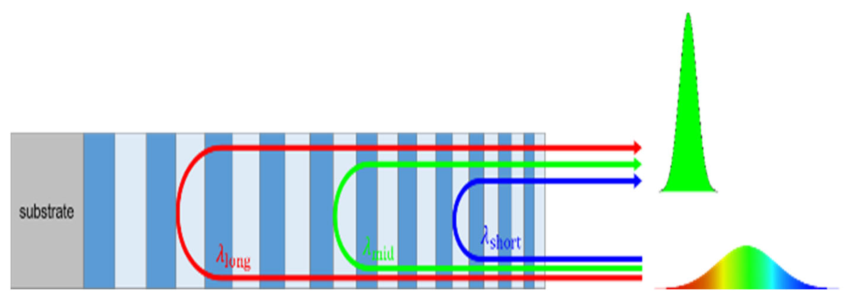
In ultrafast lasers, the generation of ultrashort pulses is based on three fundamental parts: (1) gain medium, (2) mode-locking mechanism, and (3) dispersion compensation design. When ultrashort laser pulses consisting of a spectrum in various wavelengths pass through the dispersive medium, each component exhibits different group delays due to the dispersions in the medium; hence, the broad pulse width is inevitable and consequential. In the oscillator of a solid-state ultrafast laser, the initial pulse formed by the mode-locked mechanism is consistently amplified by the gain medium until reaching steady-state power; and, these pulses travel back and forth along the same wave path across the gain medium block. In conventional design, optical components made of fused silica are used to transmit the pulses; hence, the optical dispersions will deteriorate the pulse shape in broadened pulse width due to the effects of group delay dispersion (GDD) and other higher-order dispersions. To effectively control the pulse shape from the oscillator, the effects of dispersion must be eradicated by inserting optical elements with opposite signs in dispersion coefficient into the path, technically in optics called dispersion compensation. The dispersion compensation approach based on angular dispersion, such as grating pairs and prism pairs, has been reported and applied to ultrafast laser systems for some years. However, due to bandwidth limitations and other intrinsic disadvantages, they are incapable of meeting the needs of the advanced ultrafast laser systems nowadays. The chirped mirrors, proposed by Szipöcs et al., in 1994 [3,4], are based on the difference in path length resulting from the wavelength-dependent penetration depth in the multilayer structure in order to generate negative dispersion effects. Figure 1 illustrates the concept of a chirped mirror in a schematic depiction. Compared with other dispersion compensation elements such as grating and prism pairs, negative dispersion mirrors are more advantageous in low losses, less nonlinear effects, ultra-broadband, high compactness, simple installation, and easy adjustment. Hence, it has become the mainstream dispersion compensation component in ultrafast lasers today.
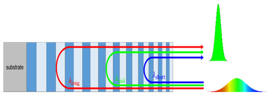
Figure 1.
Schematic of the concept for chirped mirrors.
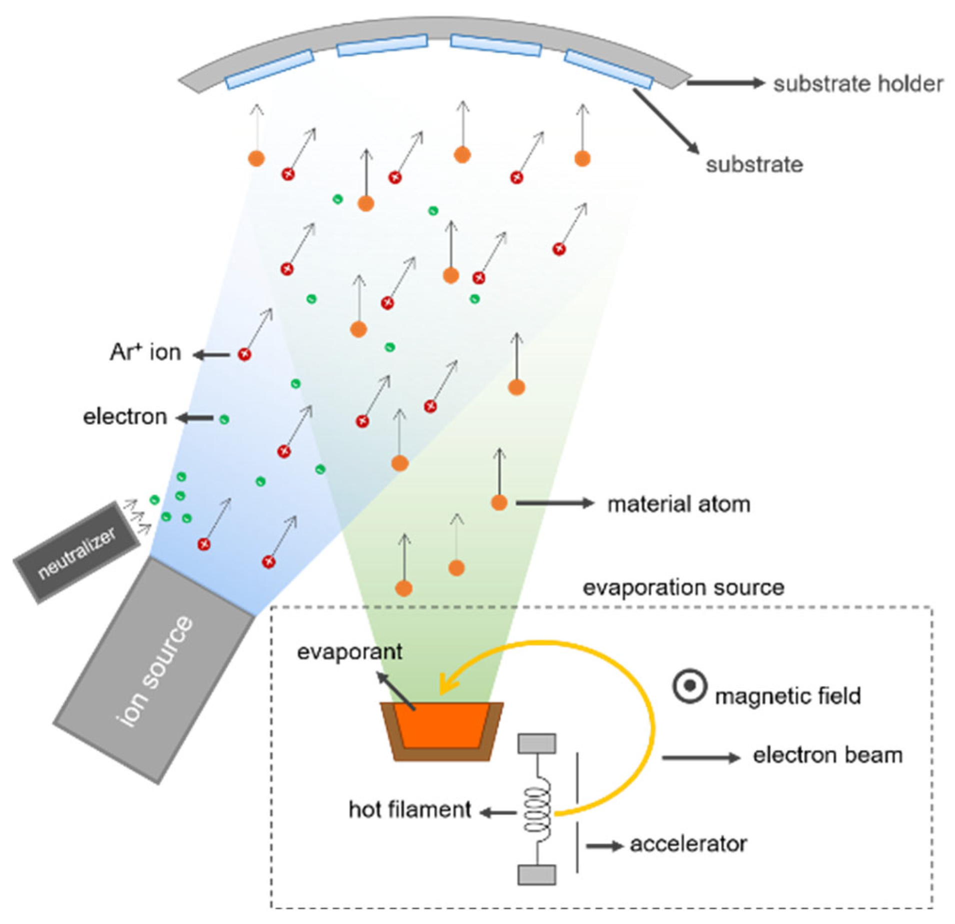
As the manufacture of chirped mirrors requires accurate control of film thickness and refractive index, various sputtering methods, namely ion beam sputtering and magnetron sputtering, have been dominant in the mass production of chirped mirrors. However, the sputtering mechanism is well known for its high costs and lack of mass production capability [5]. Since many recent advancements have been made in IAD coaters, studies of mass production of coated mirrors in laser applications have been reported elsewhere [6]. The objective of this paper is to investigate the feasibility of using IAD in the mass production of chirped mirrors mounted on a large umbrella-shaped substrate holder as shown in Figure 2.

Figure 2.
Schematic drawing of an ion-assisted electron-beam evaporation coating system.
2. Optics Theory in Thin Film
2.1. Calculation of Dispersion
In the fundamental theories of geometric and physical optics, dispersion is defined as the wave propagation relationship between the wavenumber k (or the wavelength λ = 2 π/k) and the angular frequency ω. Furthermore, the refractive index of optical materials is defined as the ratio of light speed in a vacuum to the light speed traveling in the material as follows:
From the definition of wavenumber, the dispersion of material can be derived as follows:
and the spectral phase shift is equal to the product of wavenumber and the length in the dispersive medium:
To quantify the material dispersion, Taylor Series expansion at the central frequency of the wavenumber are adopted and derived as follows:
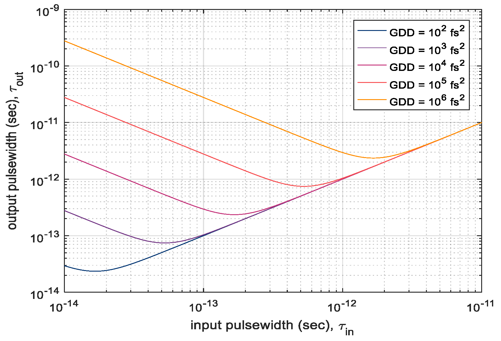
where the second-order derivative is GDD that causes the pulse-broadening effect. The quantitative description of pulse-broadening effects with respect to GDD can be described as follows.
Hence, the characteristics of output pulse width versus input pulse width can be plotted in a logarithmic scale as shown in Figure 3 for the given GDD values.
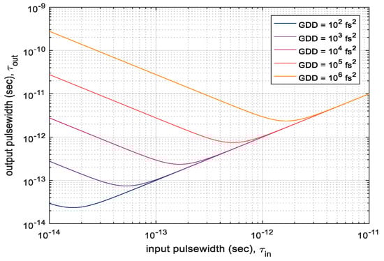
Figure 3.
Plots of curves on broadened output pulse width versus input pulse width at various GDD values.
2.2. Thin Film Theory
Since every single thin film layer can be regarded as a single interface in geometric optics, a multilayer thin film can also be treated as an iterative operation of multiple interfaces. The characteristic matrix of an assembly of layers is hereby defined as follows:
where and are the optical admittance and the phase thickness of the -th layer. In the braces of the above equation, it can be expressed as products of characteristic matrices of the layer 1 to m; i.e., . On the other hand, B and C are the normalized tangential electric field and magnetic field at the front surface. Hence, the equivalent optical admittance of the assembly is given by:
Hence, the simplified multi-film representation is shown in Figure 4 to be a single interface. With the characteristic matrix of assembly, the reflectance and the spectral phase of reflection of the film assembly can be calculated by the following equations:
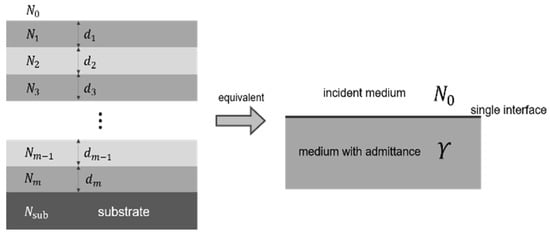
Figure 4.
Simplified representation of a thin film multilayer to a single interface.
2.3. Mirror Dispersion
In general, the design of filters based on multilayer thin film focuses on the spectral intensity properties without specifications on the spectral phase. A dispersive mirror needs to provide chromatic dispersion for dispersion compensation in GDD in ultrafast laser applications. Therefore, the dispersive mirror must provide two unique characteristics; namely, they are constant GDD in bandwidth and negative signs for the cancellation of dispersion of the material. In addition, the dispersive mirror is assumed to be linear so that the laser pulse can bounce back and forth to achieve a large amount of dispersions.
According to the definition of GDD in the previous section, GDD is the second-order partial derivative of the spectral phase; and, the GDD of a thin film assembly can be determined as follows:
3. Optical Miror Design
3.1. Merit Function
The merit function proposed by Baumeister in 1958 [7] can quantitatively evaluate the proximity of the spectral characteristics between the optical multilayer thin film and the target requirements. The method leads the thin film design to be formulated as optimization problems. The form of the merit function can be written as the form of a weighted squared difference:
which includes the film design value , the target value , and the corresponding tolerance of the optical property value on the spectrum. The smaller the value calculated by the merit function, the closer the design approaches the design goal. In the optimization of chirped mirrors with target bandwidth, two design objectives must be met both in high reflectance and at a GDD value so that the merit function is defined in the following:
It is noted that the above merit function considers both the reflectance and the GDD of the chirped mirror with a multilayer thin film.
3.2. Needle Optimization
In optimization theory, the most troublesome issue is to determine the existence of local minima in the given domain. This is especially cumbersome in the multilayer thin film optimization problems due to the under-constraint conditions. Many algorithms are available for the optimization of film thickness design of chirped mirrors published recently [8,9,10]; however, the most notable and conventional method is the needle optimization method proposed by Tikhonravov in 1982 to verify the capability of optimization in the number of layers in shop practice [11,12,13]; additionally, in some specific problems, the method can even directly start from a single layer without an appropriate initial number of layers. Since many mass production coater systems are customer-made with a limited number of materials crucibles and monitoring glass substrates, a fast and reliable optimization method should be selected for this study.
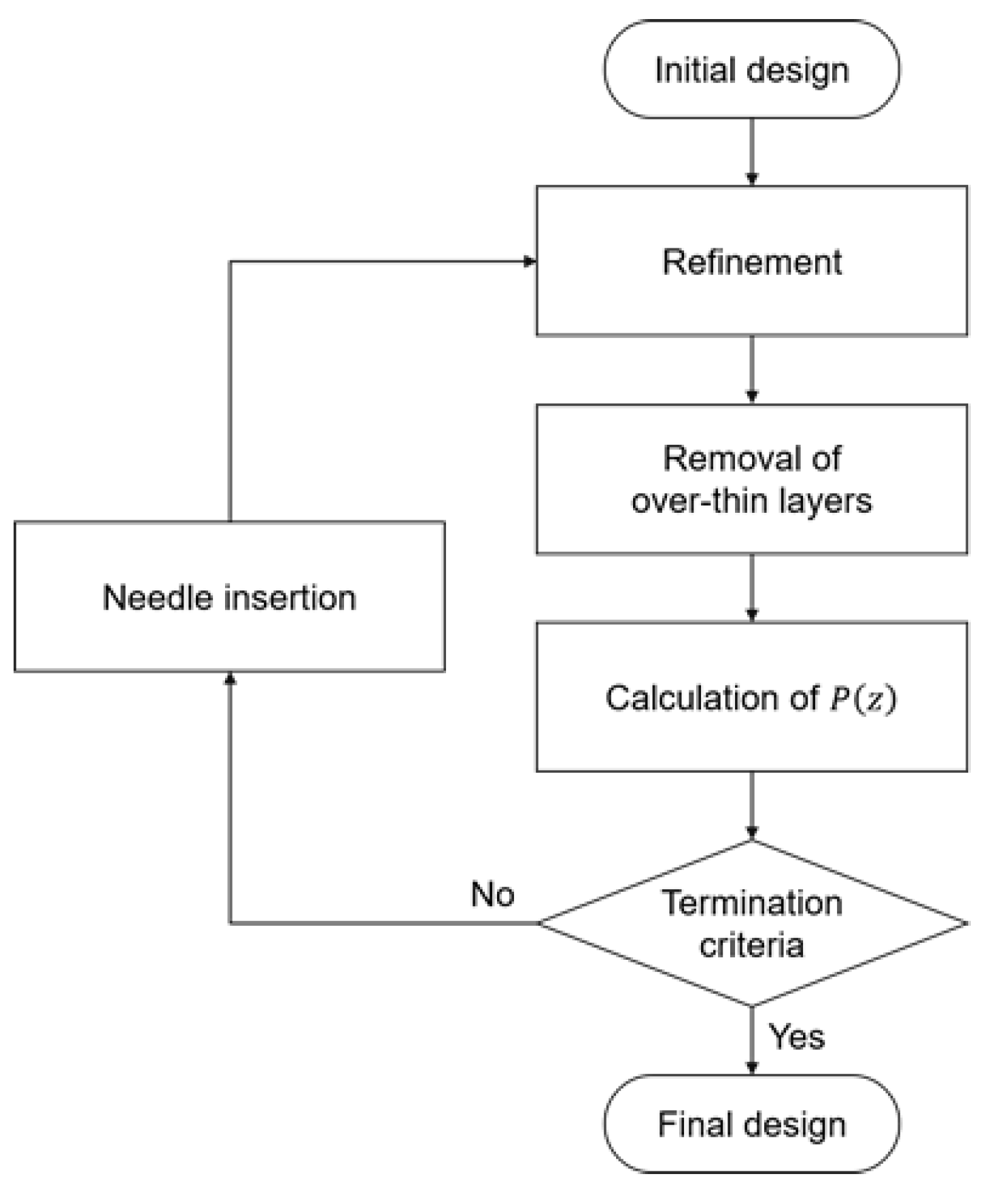
The main concept of needle optimization is by inserting new layers into the existing design to optimize the merit function. In the original design, a function P(z) can be calculated and it means the change in the merit function corresponding to a single needle variation added at location z:
and P(z) can be calculated through an analytic method [14].
P(z) = ΔF
Figure 5 illustrates the design flowchart of the needle optimization algorithm with steps in refinement, removing over-thin layers, calculating the P function, termination criteria, and insertion of needle layers in total. When the termination condition is not met due to the removal of over-thin layers, either a random fluctuation of thickness can be added during the optimization or the thickness of the layers can be locked before the over-thin condition happens.

Figure 5.
The flowchart of the needle optimization algorithm by Tikhonravov et al. [11].
3.3. Mirror Design
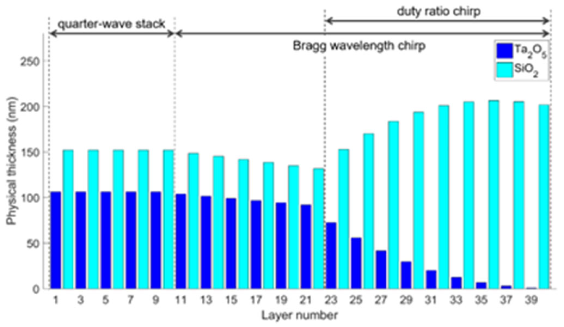
In this study, an open-source program, published by Larouche and Ludvik in 2008 named as OpenFilters, for optical thin film design and analysis is employed [15]. In the paper published by Pervak et al. [16], the suggested design steps illustrate the specific selected initial designs can be very helpful for finding a good and achievable solution. Accordingly, a 40-layer double-chirped mirror (DCM) structure is selected as the initial design with the film thicknesses corresponding to the 40 layers shown in Figure 6. It is noted that three regions of layers are designated to fulfill the optimization of merit function according to the results from the literature review.

Figure 6.
Layer thicknesses in the DCM at the initial design.
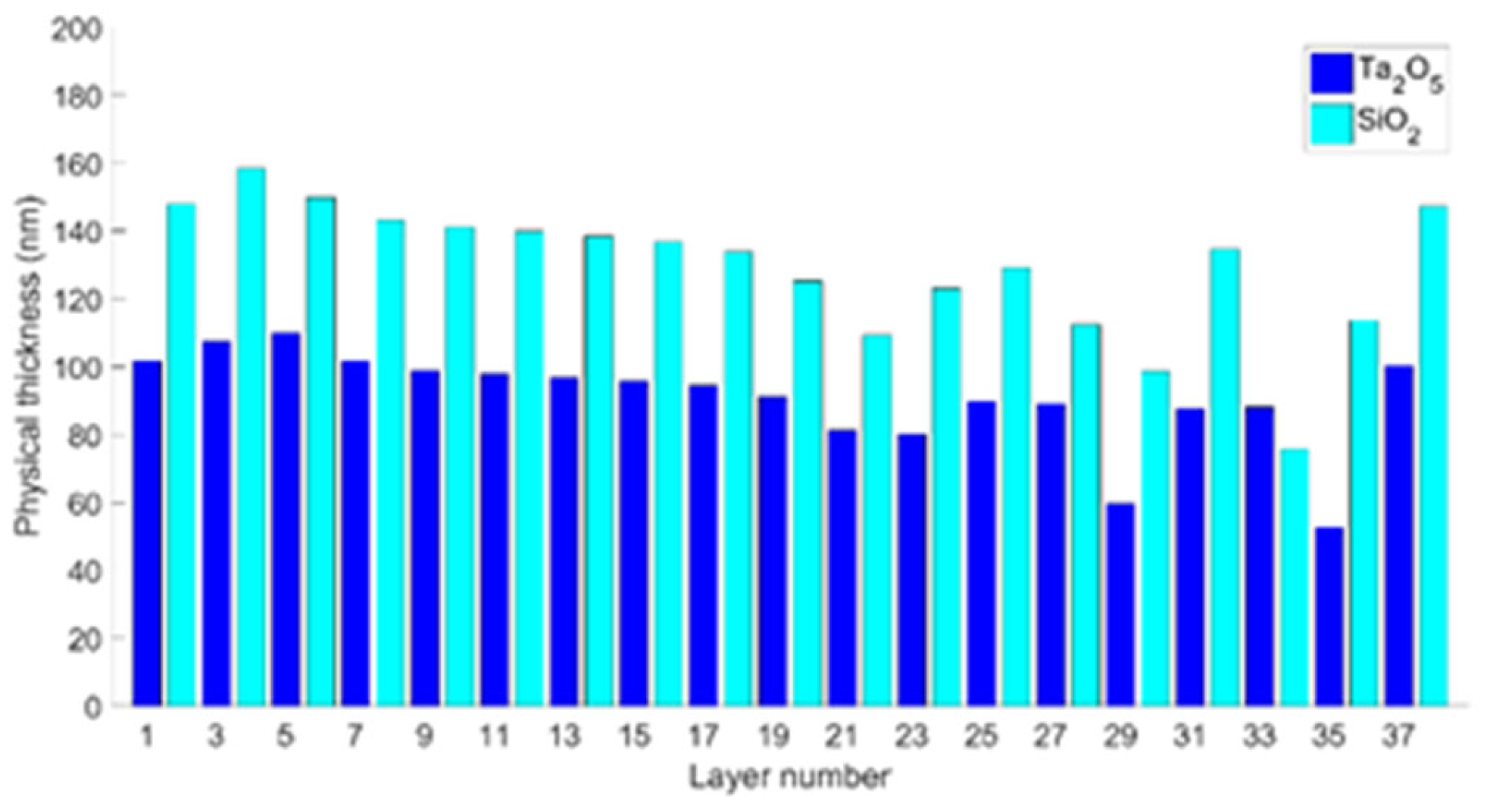
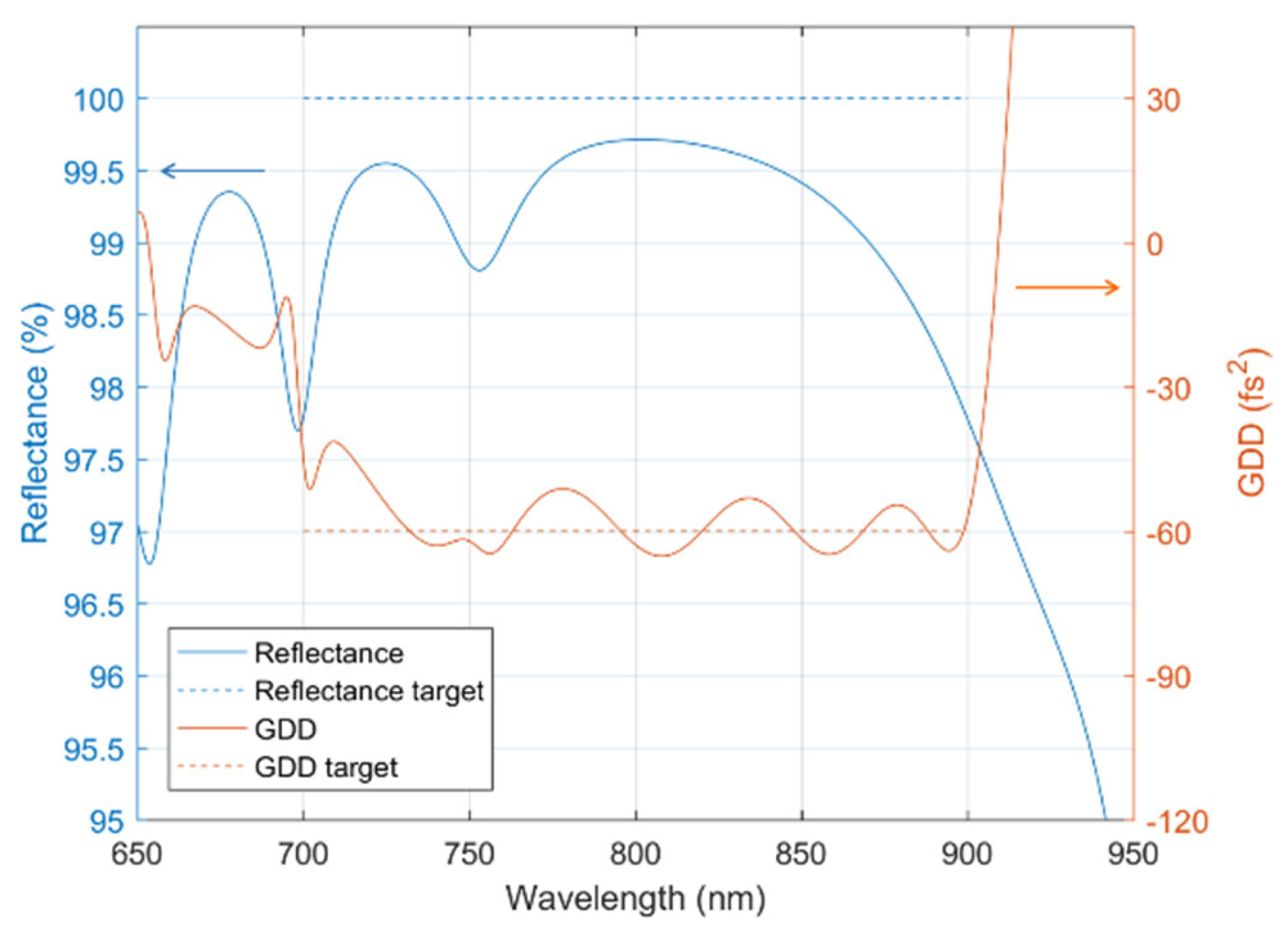
Before the optimization scheme is applied, the initial thicknesses of the high and low index of material are selected based on the experimental data from the calibration runs described in the following section. Fed with the initial design values, the needle optimization program calculates the output data plotted with layer thickness as shown in Figure 7. The calculation speed and convergence of the program give reliable film thickness with less difference between H and L material. Figure 8 plots the corresponding reflectance and GDD versus wavelength of the optimal design that meets the merit function defined for this study.
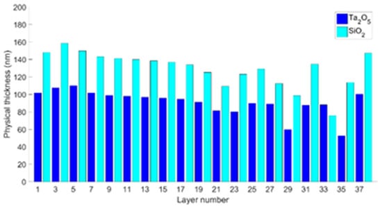
Figure 7.
Layer thicknesses in the DCM in the final design.
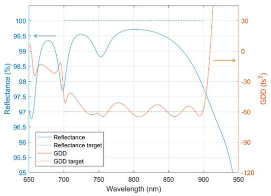
Figure 8.
Plots of optical properties of the coatings vs. wavelength of the optimal film design.
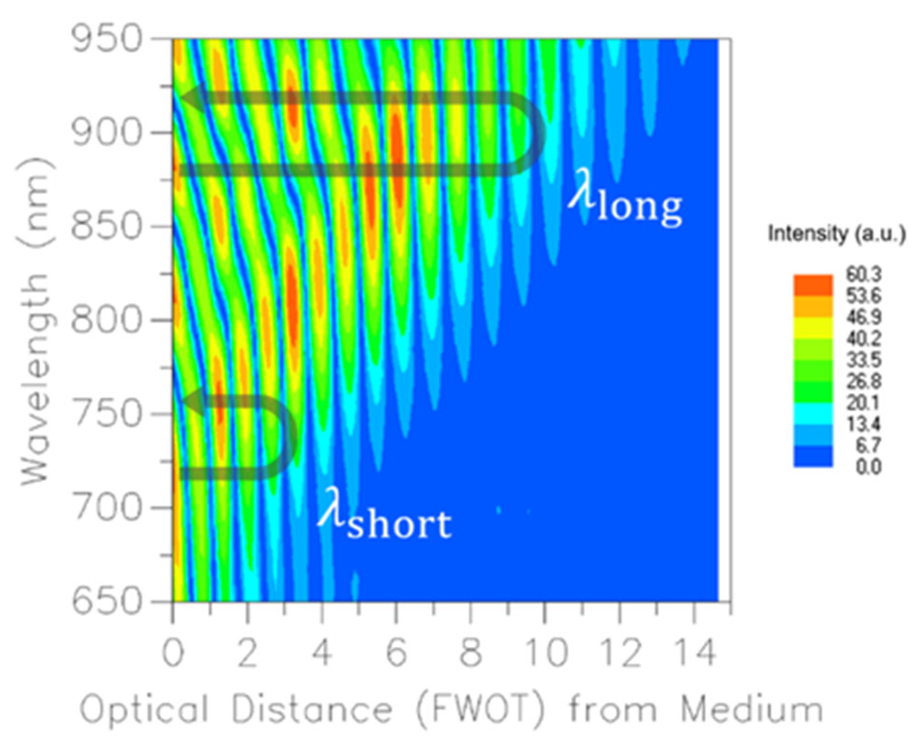
To further verify the optimal design, Figure 9 shows the simulated electric field intensity distributions from 650 to 950 nm inside the mirror coatings plotted versus the optical distance generated by a commercial thin film software, Essential Macleod copyrighted by Thin Film Center Inc. In the figure, the longer wavelength components penetrate deeper into the structure which is well described by the theory of chirped mirror in the previous section. From the results of optimal multilayer thin film design, the operational hours of the coater system show that many environmental disturbances may influence the actual thickness of the film during the complete process. As a further step, it is evident that the study of environmental disturbances during the long-hour operation of the coater system may further confirm the final optical performance of the chirped mirror. Hence, the performance deviations due to the thickness errors with normal Gaussian distributions at 1.0% are entered into each layer of the optimal design thickness for more than hundreds of simulation cases.

Figure 9.
Simulated electric field distribution in the film structure versus wavelength.
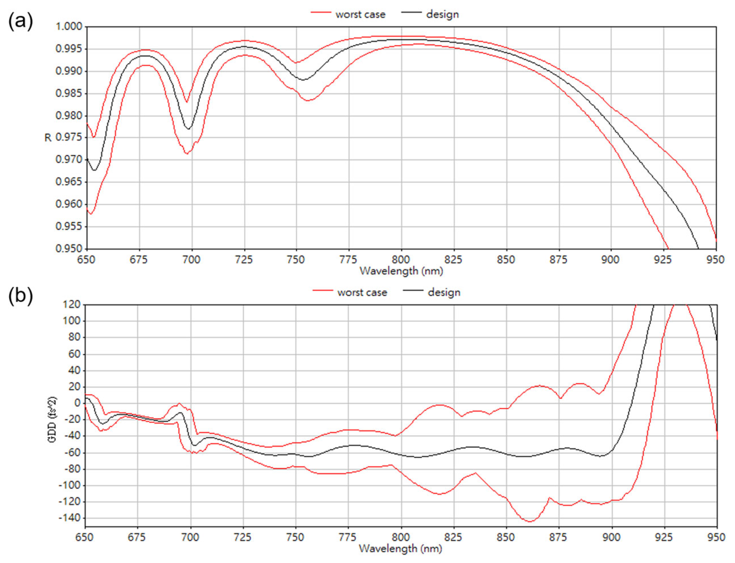
After analysis of the simulated data, the corresponding simulated results are plotted in Figure 10 in which the design targets and the bandwidth regions are well enclosed by the worst-case scenario. The simulated results indicate when the wavelength is longer than 800 nm, the deviations in GDD may not be controlled at a constant. However, when the wavelength is smaller than 800 nm, the deviations in GDD should stay almost at a constant value down to 700 nm. This part of the simulations may be useful to verify the experimental results if similar observations are shown in the GDD plots.
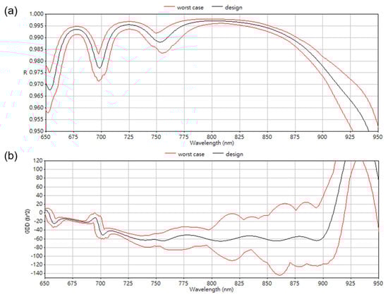
Figure 10.
Simulated effects in optical properties at 1% normal Gaussian distribution for each layer thickness error. (a) Reflectance response, (b) GDD response.
4. Design Verifications and Experimental Results
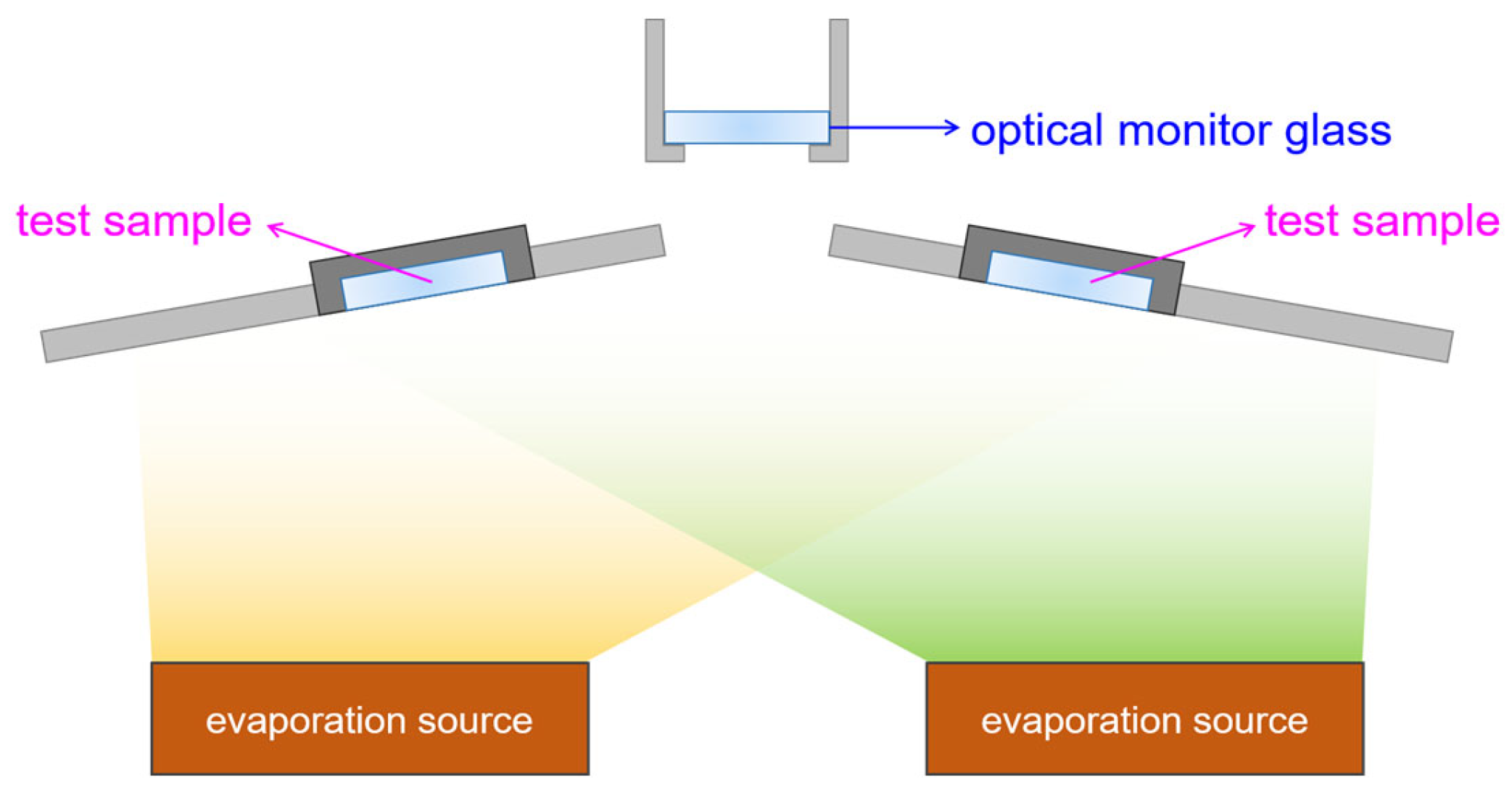
The IAD apparatus used in this study is a customer-specific machine, Model: SGC-22SA-IAD, made by Showa Shinku Co., Sagamihara, Japan. Two electron guns, made by JEOL Co., are used for the individual hearths of material placed in copper crucibles. A Veeco® ion source, made in New York, NY, USA, generates the plasma used on the targets. Both crystal and optical monitoring devices are embedded on the top of the target umbrella for film thickness control. Table 1 lists the pertinent process parameters of high (Ta2O5) and low (SiO2) refractive index materials, both manufactured by Canon OPTRON, Tokyo, Japan, used on the IAD apparatus. Since the geometry and design of the apparatus are different in various models as shown in Figure 11, there are calibration factors needed for the computer controller before any normal coating cycle can be started.

Table 1.
Pertinent process parameters of Ta2O5 and SiO2.
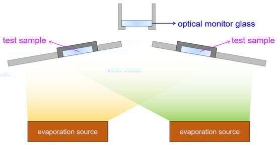
Figure 11.
Schematic drawing for showing location differences among test samples and optical monitoring sensor.
It should be noted that the basic calibration factors, namely the optical constants of coated films and the tooling factors due to the different locations of the targets and sensors, must be correctly determined by trial runs for the materials. Hence, preliminary trial runs of the experiment were conducted for correlating the above factors by analysis of experimental data. First, Ta2O5 and SiO2 were individually coated on optical grade BK7 glass substrates (Unice EO Inc., Taoyuan, Taiwan) with 25 mm in diameter, and 1.0 mm in thickness with surface roughness better than 1 nm. Based on the total periods of the coating process and minimum control in time steps of the controller, single-layer film thicknesses of 10, 50, and 100 nm were selected for the calibration runs for both materials. A total number of eight samples on a holding plate of the umbrella were coated in a trial run. More than a hundred trail samples were made for the calibration process.
As a further step, the thickness and optical constants (i.e., refractive index spectrum) of groups of eight samples were measured and analyzed by a in-house built variable-angle spectroscopic ellipsometer (VASE). The details of the technique in VASE measurements are considered trivial here since the steps are tedious and standardized in optical film measurement technology [17]. As a result, the analysis results showed that samples coated at 50 nm and 100 nm settings for both materials are similar in refractive indices and tooling factors illustrated in Table 2 and Table 3. In the tables, it is noted that the samples coated at 10 nm show unacceptable variations due to the rationale of possible deposition defects and dependence of refractive index on extra-thin thickness. Therefore, in the early design stage, the layers with thicknesses smaller than 50 nm were removed from the design procedure to carefully define the lower limit of the optimization method to coat the chirped mirror with confidence.
Table 2.
Analysis results of single-layer Ta2O5 film coated with various thicknesses.
Table 3.
Analysis results of single-layer SiO2 film coated with various thicknesses.
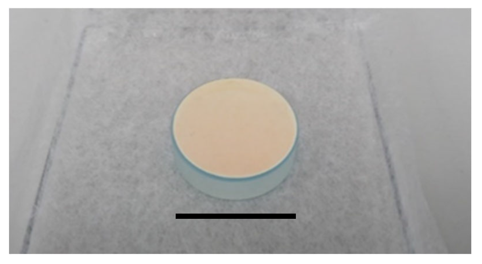
Based on the analysis of VASE measurements, the coating process parameters were re-entered into the IAD system controller (manufacturer, city, country), the complete coating process was automatically conducted on the IAD apparatus. From warm-start to cool-down, the total coating process required approximately 26 h. Figure 12 shows the photo picture of a coated chirped mirror with 25 mm in diameter and 5.0 mm in thickness.
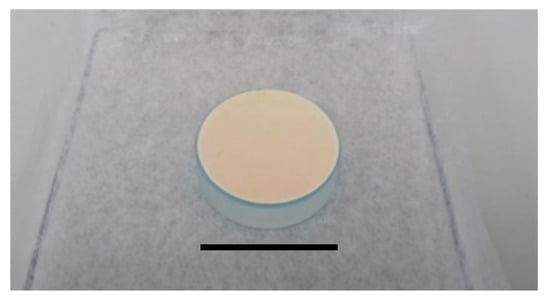
Figure 12.
Photo picture of a coated chirped mirror; black line is 25 mm in length.
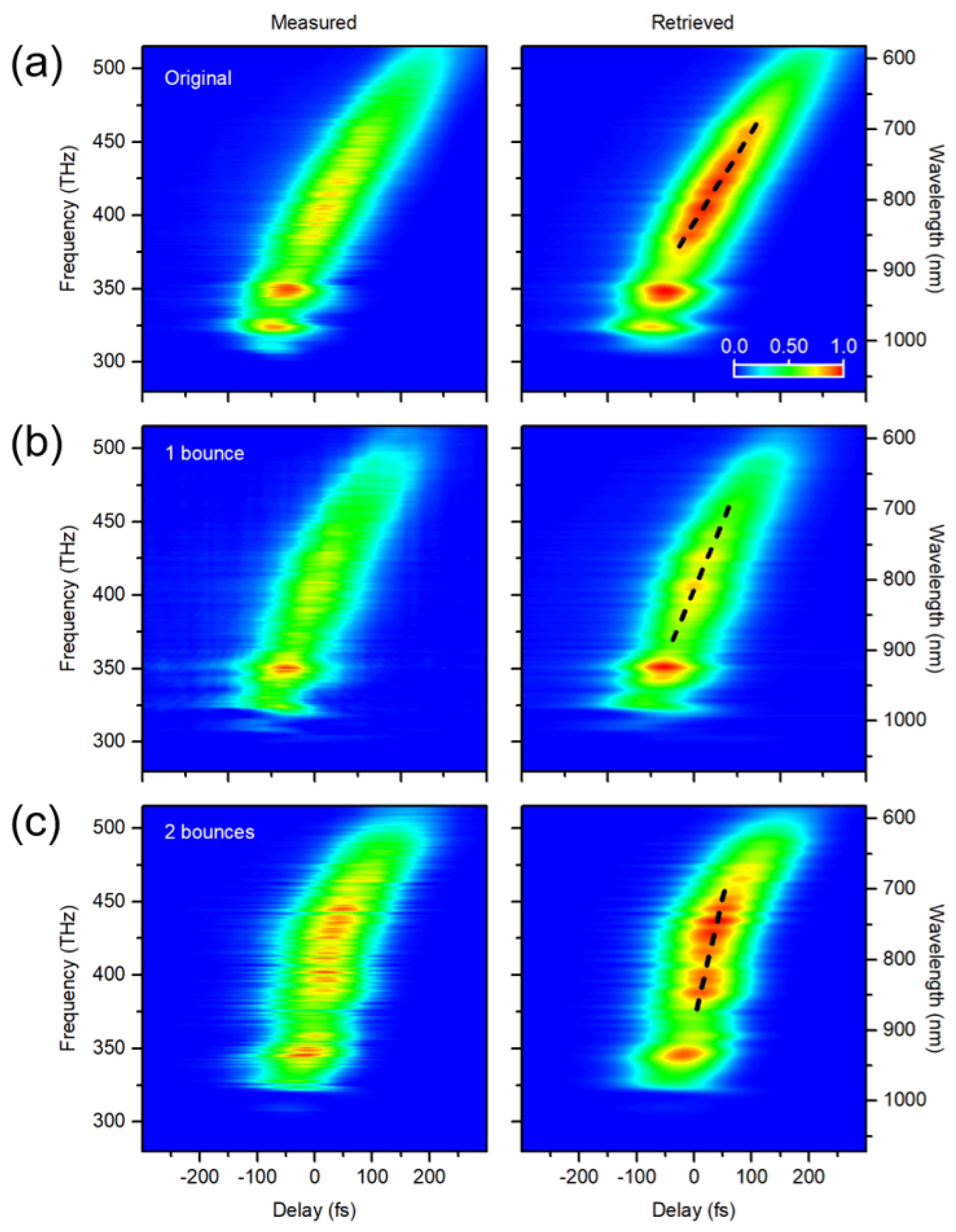
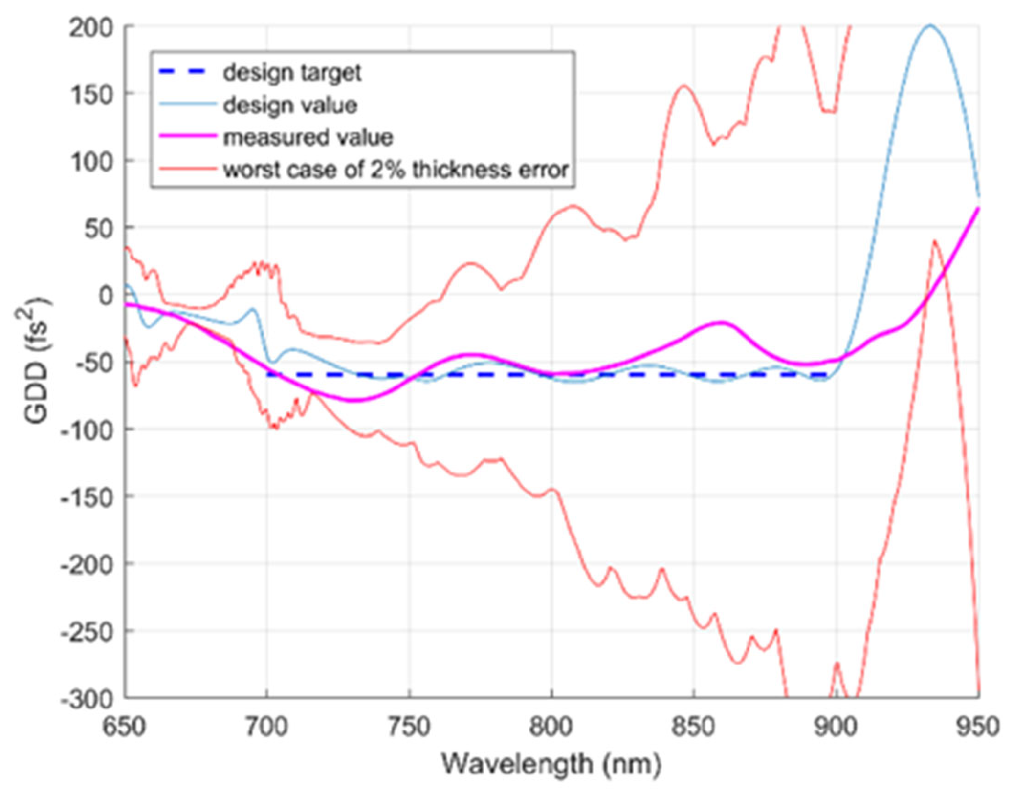
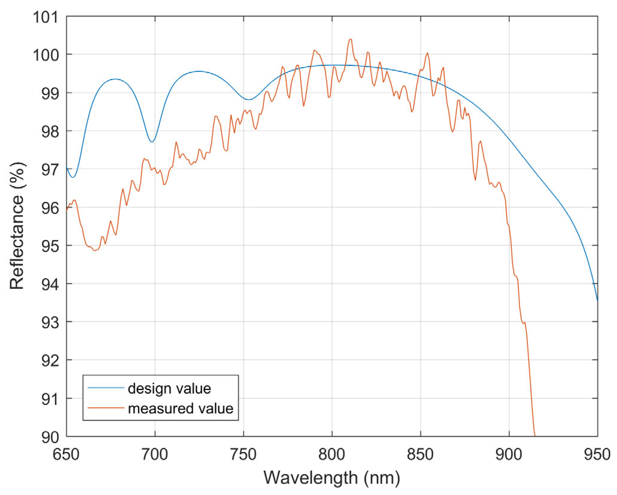
To check for the performance of the coated chirped mirrors, the reflection spectrum including intensity and phase is measured by the polarization gating frequency-resolved optical gating (PG-FROG) method [18]. The PF-FROG measurement results are shown in Figure 13 in which the retrieved plots show pulse becomes less delayed after bouncing on the chirped mirror. In Figure 14, the pulse temporal data plots indicate pulse width being reduced after bouncing on the chirped mirror. In a further analysis by the use of Taylor Series expansions in the spectral differences between the original pulse and the bounced pulse from the chirped mirror, the GDD values of the chirped mirror can be plotted as shown in Figure 15 in which the measured GDD values agree well with the design target and values; additionally, they are bounded by the worst-case scenario of GDD deviations at thickness error of 2% in the wavelength from 700 to 900 nm. Finally, Figure 16 shows the plots with a comparison between the VASE reflectance measurements and the design values. An average of 2% in scattering losses are observed. Again, this confirms the fabricated chirped mirrors could meet the specifications given by the optimal design results.
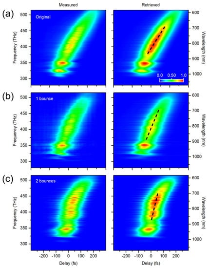
Figure 13.
Trace plots of PG-FROG measurements: (a) properties of original pulse, (b) properties of pulse after 1 bounce, and (c) properties of pulse after 2 bounces.
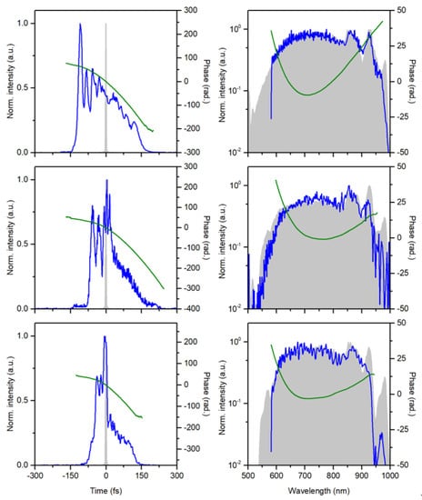
Figure 14.
Temporal and spectral plots of PG-FROG measurements corresponding to Figure 13.

Figure 15.
Comparisons of the GDD response among the design target, the design values, the measured values, and bound of GDD deviations under the worst-case scenario of thickness error at 2%.
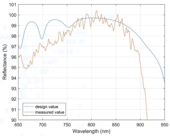
Figure 16.
Comparisons of the plots between the measured reflectance and the optimal design values showing an average of 2% extra losses due to scattering.
5. Conclusions
In this paper, theoretical derivations in the design of chirped mirrors employed for ultrafast lasers are introduced with an easy-to-implement design optimization method. Furthermore, the popular IAD coating method is employed for experimental verifications of the optimal design of chirped mirrors with comprehensive descriptions of the calibration steps and experimental measurement results. First, the optical constants and the tooling factors of coating materials are measured for the two selected materials, namely Ta2O5 and SiO2. With the minimum layer thickness being set at 50 nm, the film thickness of all layers was coated in approximately 24 h to produce a batch of eight mirrors for verification purposes. Both the PG-FROM measurements and reflectance plots confirm that the proposed mass production of chirped mirrors is feasible with the commercially well-developed ion-assisted e-beam evaporation process. The temporal and spectral measurements illustrate the chirped mirrors fabricated by this method can meet the ultrafast laser requirements. Nevertheless, the simulated results in Figure 15 indicate careful monitoring and control of the environmental factors that influence the physical coating mechanism should be an important practice to be conducted on the shop floor.
In conclusion, when considering the equipment costs and mass production capability, the IAD coating systems are possible candidates for meeting the needs in the large volume production of chirped mirrors for the ultrafast laser industry. Since many tedious experimental steps are necessary for the calibration of the IAD coating method, a systematic method of design and fabrication of chirped mirrors should be studied with comprehensive theoretical and experimental results. Furthermore, it should also be noted that the economic advantages of the mass-produced chirped mirrors cloud also propel the progress in industrial applications of ultrafast laser systems.
Author Contributions
Y.-L.C. conducted the calculations and experimental preparation, execution, and measurements; and, he also downloaded the open-source codes from the public domain with minor modifications in order to fit the limits of the coaters in the lab. P.-J.W. and Y.-L.C. discussed and checked the validity of the analysis results and experimental results together to prepare the manuscript for submission. All authors have read and agreed to the published version of the manuscript.
Funding
This research received no external funding from organizations and institutes other than the university with which the authors were all affiliated.
Institutional Review Board Statement
Not applicable.
Informed Consent Statement
Not applicable.
Data Availability Statement
The data reported in the paper can be found on the national thesis archive on the web address https://hdl.handle.net/11296/25ct2g (accessed on 28 December 2022).
Acknowledgments
The authors want to thank Largan Precision Co. Ltd., Taichung Taiwan, for the IAD coaters used in this paper with basic support of operational costs. Special thanks are due to Yang Shang-Da and Chen Bo-Han and Lu Chih-Hsuan from the Ultrafast Photonics Laboratory at NTHU for providing help on the PG-FROG measurements.
Conflicts of Interest
The authors declare no conflict of interest. The funders had no role in the design of the study; in the collection, analyses, or interpretation of data; in the writing of the manuscript; or in the decision to publish the results.
References
- Sugioka, K.; Cheng, Y. Ultrafast lasers—Reliable tools for advanced materials processing. Light Sci. Appl. 2014, 3, e149. [Google Scholar] [CrossRef]
- Phillips, K.C.; Gandhi, H.H.; Mazur, E.; Sundaram, S. Ultrafast laser processing of materials: A review. Adv. Opt. Photonics 2015, 7, 684–712. [Google Scholar] [CrossRef]
- Jena, S.; Tokas, R.B.; Sakar, P.; Misal, J.S.; Maidul Haque, S.; Rao, K.D.; Thakur, S.; Sshoo, N.K. Omnidirectional photonic band gap in magnetron sputtered TiO2/SiO2 one dimensional photonic crystal. Thin Solid Films 2016, 599, 138–144. [Google Scholar] [CrossRef]
- Szipöcs, R.; Ferencz, K.; Spielmann, C.; Krausz, F. Chirped multilayer coatings for broadband dispersion control in femtosecond lasers. Opt. Lett. 1994, 19, 201–203. [Google Scholar] [CrossRef]
- Amochkina, T.; Trubetskov, M. Designing broadband dispersive mirrors in the mid-infrared spectral range: A theoretical study. Appl. Opt. 2023, 62, B63–B72. [Google Scholar] [CrossRef]
- Grigoriev, F.G.; Sulimov, V.B.; Tikhonaravov, A.V. Atomistic simulation of the ion-assisted deposition of silicon dioxide thin film. Nanomaterials 2022, 12, 3242. [Google Scholar] [CrossRef] [PubMed]
- Baumeister, P. Design of multilayer filters by successive approximations. J. Opt. Soc. Am. 1958, 48, 955–958. [Google Scholar] [CrossRef]
- Ariza-Flores, A.D.; Gaggero-Sager, L.M.; Agarwal, V. White metal-like omnidirectional mirror from porous silicon dielectric multilayers. Appl. Phys. Lett. 2012, 101, 03119. [Google Scholar] [CrossRef]
- Dems, M.; Wnuk, P.; Wasylczyk, P.; Zinkiewicz, L.; Wojcik-Jedlinska, A.; Reginski, K.; Hejduk, K.; Jasik, A. Optimization of broadband semiconductor chirped mirrors with genetic algorithm. Appl. Phys. B 2016, 122, 266. [Google Scholar] [CrossRef]
- Ortiz-Vazquez, E.; Lujan-Cabrera, I.A.; Isaza, C.; Rizzo-Sierra, J.A.; Ramirez-Gutierrez, C.F. Design of broadband modulated one-dimensional photonic crystal based on porous silicon using evolutionary search. Optik 2022, 260, 169002. [Google Scholar] [CrossRef]
- Tikhonravov, A.V. Synthesis of optical coatings using optimality conditions. Vestn. MGU Phys. Astron. Ser. 1982, 23, 91–93. [Google Scholar]
- Tikhonravov, A.V.; Trubetskov, M.K.; DeBell, G.W. Application of the needle optimization technique to the design of optical coatings. Appl. Opt. 1996, 35, 5493–5508. [Google Scholar] [CrossRef] [PubMed]
- Tikhonravov, A.V.; Trubetskov, M.K.; DeBell, G.W. Optical coating design approaches based on the needle optimization technique. Appl. Opt. 2007, 46, 704–710. [Google Scholar] [CrossRef] [PubMed]
- Furman, S.A.; Tikhonravov, A.V. Basics of Optics of Multilayer Systems; Atlantica Séguier Frontieres: Biarritz, France, 1992. [Google Scholar]
- Larouche, S.; Martinu, L. OpenFilters: Open-source software for the design, optimization, and synthesis of optical filters. Appl. Opt. 2008, 47, C219–C230. [Google Scholar] [CrossRef] [PubMed]
- Pervak, V.; Razskazovskaya, O.; Angelov, I.B.; Vodopyanov, K.L.; Trubetskov, M. Dispersive mirror technology for ultrafast lasers in the range 220–4500 nm. Adv. Opt. Technol. 2014, 3, 55–63. [Google Scholar] [CrossRef]
- Woollam, J.A.; Johns, B.D.; Herzinger, C.M.; Hilfiker, J.N.; Synowicki, R.A.; Bungay, C.L. Overview of variable-angle spectroscopic ellipsometry (VASE): I. Basic theory and typical applications. In Optical Metrology: A Critical Review; SPIE: Bellingham, WA, USA, 1999; Volume 10294, p. 1029402. [Google Scholar]
- Trebino, R.; Kane, D.J. Using phase retrieval to measure the intensity and phase of ultrashort pulses: Frequency-resolved optical gating. J. Opt. Soc. Am. A 1993, 10, 1101–1111. [Google Scholar] [CrossRef]


Disclaimer/Publisher’s Note: The statements, opinions and data contained in all publications are solely those of the individual author(s) and contributor(s) and not of MDPI and/or the editor(s). MDPI and/or the editor(s) disclaim responsibility for any injury to people or property resulting from any ideas, methods, instructions or products referred to in the content. |
© 2023 by the authors. Licensee MDPI, Basel, Switzerland. This article is an open access article distributed under the terms and conditions of the Creative Commons Attribution (CC BY) license (https://creativecommons.org/licenses/by/4.0/).