Abstract
To improve laser-capture microdissection (LCM) resolution, we designed a near-field probe LCM system that pushed microdissection resolution from 7.5 μm to 400 nm. Here, we report a transfer film for our constructed system, replacing commercial transfer films used in conventional LCM systems. A low-melting-point ethylene vinyl acetate (EVA) copolymer was chosen as the main material. Adequate concentrations of EVA and near-infrared (NIR) absorbing dyes of an appropriate thickness to prepare the transfer film were investigated. The flatness of the film surface and the relationship between different film thicknesses and melt dot sizes were studied using atomic force microscopy and scanning electron microscopy, respectively. The results show that the flatness is approximately 4.3 nm, and the melt dot size is proportional to the transfer film’s thickness. The proper conditions for preparing the film were 17.5% (w/v) of EVA in the toluene solution with 0.001 M of NIR absorbing dyes. Using a 30 μm thick transfer film, 200 nm diameter particles on a 20 nm thick monolayer of gold particles could be captured.
1. Introduction
The first laser-capture microdissection (LCM) system was reported by Emmert-Buck and coworkers in 1996 [1]. Today, these systems are widely used to obtain pure cell populations from tissue sections [2,3,4], and have become widely adopted in molecular pathology. The resolution of a typical commercial LCM system is approximately 7.5 μm, which is sufficient for isolating mammalian cells. However, conventional LCM systems cannot enable submicrometer laser manipulation, which is required for many applications in biomedical research. Therefore, nano-manipulation of deoxyribonucleic acid (DNA) using atomic force microscopy (AFM), combined with ultraviolet (UV)-laser micro-beams, has been reported [5]. On one hand, sub-400 nm cuts were achieved; on the other hand, DNA damage was likely incurred by UV-laser beam exposure.
To achieve the non-damaging nanodissection of biological specimens, we designed and reported a near-field probe LCM system, which improved capture resolution from 7.5 μm to 400 nm [6]. In every LCM system, the transfer film is the main component of dissection; the transfer film converts light into heat and melts partly by absorbing the irradiating laser’s energy. The capture size depends on the diameter of the light dot incident on the transfer film. In a conventional LCM system, a lens is used to focus the laser. Owing to the diffraction limit, the diameter of the laser focus is proportional to the wavelength of the incident laser beam and inversely proportional to the numerical aperture of the lens. To improve the resolution, we established a near-field probe LCM system by replacing the conventional focusing lens with a fiber tip [6]. The fiber tip was mounted on a 2D nanometer piezo actuator for the precise capturing of the target sample. An 808 nm laser was introduced into the fiber to locally heat and melt the transfer film right above the target. The near-field fiber tip (with a 150 nm aperture diameter) reduced the size of the light dot by one order of magnitude compared to conventional LCM systems. To achieve high-resolution capture using near-field probe LCM, the distance between the tip and the film needs to be controlled to be about 1μm to reduce the light dot size while keeping enough laser energy to melt the film. To solve this problem, we designed a novel mount with a hole for the transfer film, enabling the fiber probe to exert close to melting [7]. As a result, the energy of light on the transfer film was reduced. Therefore, the thickness of the transfer film needs to be adjusted accordingly.
Additionally, conventional transfer film is made by hot-melted plastic ethylene vinyl acetate (EVA), which has a high melting temperature of about 90 °C [8]. Such high temperatures may easily damage the captured biological samples.
To address the above issues, here we optimized the processes for preparing transfer film for near-field probe LCM by choosing proper EVA materials with lower melting points and investigated the adequate concentrations of materials, film thickness, and spin-coating conditions. The prepared film was then used for the higher-resolution capture of the target particles.
2. Materials and Methods
2.1. Chemicals
The EVA copolymer with a low melting point of 65 °C (EVATHENE® UE653-04) was obtained from USI Far East Corporation (Taipei, Taiwan). Near-infrared (NIR) absorbing dye, Vanadyl 2,11,20,29-tetra-tert-butyl-2,3-naphthalocyanine, which absorbs light mainly at an 808 nm wavelength, was purchased from Sigma-Aldrich (St. Louis, MO, USA). Toluene used as the organic solvent to dissolve EVA copolymer material and NIR dye were obtained from J.T. Baker (Phillipsburg, NJ, USA). Gold colloids (diameter, 20 nm) were purchased from Sigma-Aldrich (St. Louis, MO, USA). Dichlorodimethylsilane (DCMS) was purchased from Tokyo Kasei Kogyo (Tokyo, Japan) and was used to immobilize gold nanoparticles on a glass substrate.
2.2. Selection of Materials
The transfer film was irradiated by a laser in two main steps: light absorption and hot-melt adhesion. Two issues should be considered: (1) hot-melt materials and (2) NIR absorbing dyes. Many types of hot-melt materials can be used, such as polyurethane (PU), EVA, polypropylene (PP), and polyamide (PA). These materials have the following advantages: low melting point; high adhesion; high optical transparency; high stability; and a high melt index (MI).
After the low-melting-point transfer film was melted at 65 °C, the temperature of the contact part between the film and the target cells was determined based on the melting point of the material itself. Excessively high temperatures can destroy target cells. The bond strength between the cells and tissues, as well as the adhesion strength between the cells and the glass board, should be considered simultaneously during capture [9]. Therefore, the transfer film must be sufficiently strong for capture completion. Optical transparency should be sufficiently high because a microscope is typically used to observe the location of target cells under the analyzed transfer film. The transfer film should have high chemical stability and heat endurance, and it should not produce extra chemical substances or undergo structural changes that may contaminate cells at high temperatures. The MI value is the fluidity value of processed plastic and is established by the American Society for Testing and Materials (ASTM). This index is related to the material’s viscosity, with higher values corresponding to lower viscosity and better fluidity. Owing to the application scope of transfer films, higher MI values are preferred, ensuring that the transfer films drop to the preferable depth after melting. Excessively high MI values yield relatively low viscosity to allow the target cells to stick closely when dropping.
EVA can be made by the polymerization of ethylene and vinyl acetate (Vac). A higher ratio of Vac lowers the melting point and improves optical characteristics and chemical resistance. Moreover, flexibility, elasticity, high-temperature fluidity, high weather resistance, and innocuity are required for transfer films. In this study, an EVA copolymer with a Vac content of 28% was selected. It had a low melting point of 65 °C, good transparency, and good melting fluidity (MI = 400) with a refractive index of 1.49 at an 808 nm wavelength.
In addition to its low melting point, high stability, and good optical properties, a proper transfer film should exhibit high absorbency with respect to the laser light in the LCM system to improve its ability to absorb heat for melting and reduce the effect on cells when the laser light penetrates it. An 808 nm wavelength laser diode was used in our near-field probe LCM system as the light source. Vanadyl 2, 11, 20, 29-tetra-tert-butyl-2, 3-naphthalocyanine dye was selected as the material to increase the transfer film’s ability to absorb the 808 nm wavelength near-infrared light that reached its peak value. It maintained compound stability and exerted no harmful photochemical effects when heated up to 300 °C, owing to its good anti-optics rotation and chemical stability properties.
2.3. Concentration of the EVA Solution
Toluene was used as the solvent to dissolve the EVA resin grains, and the viscosity of the EVA solution was controlled by its dosage. As the toluene proportion increased to change the solution’s viscosity, the solution ratio was selected as follows: Solution A: 7 g EVA in 20 mL toluene; Solution B: 7 g EVA in 30 mL toluene; and Solution C: 7 g EVA in 40 mL toluene. The EVA plastic grains and near-infrared absorbing dyes were dissolved uniformly to obtain different-concentration EVA solutions: 0.00025; 0.0005; 0.001; 0.0015; and 0.002 M. Additionally, the spectral absorbency was measured to determine the best dyestuff concentration to prepare the transfer film.
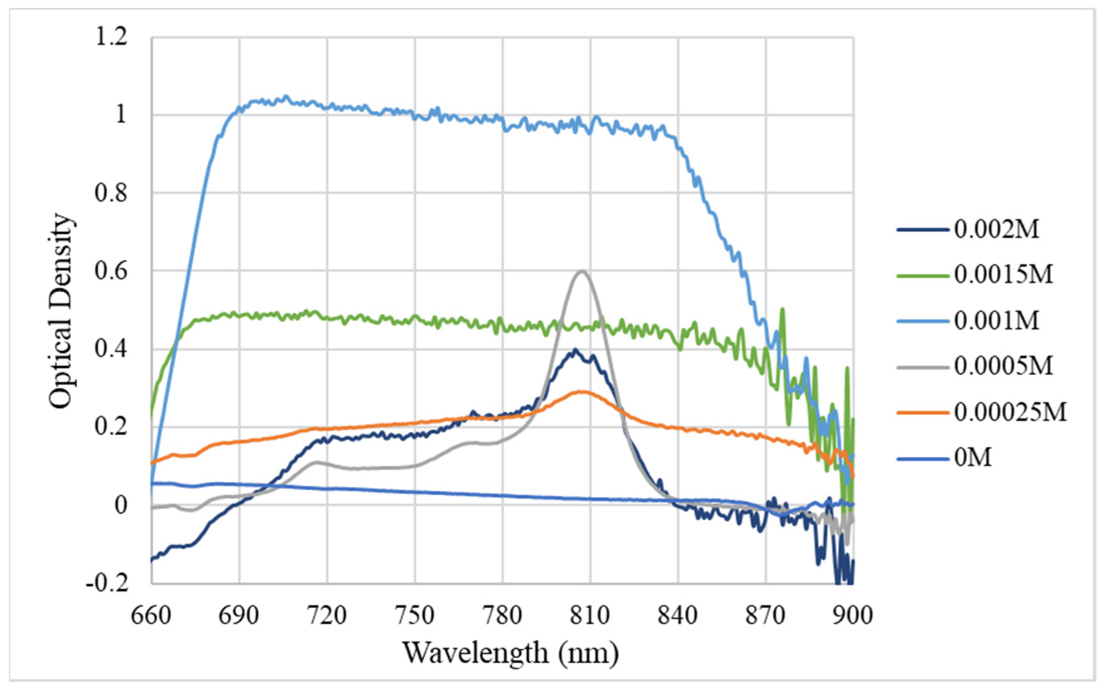
A Cary 3E UV-Vis Spectrometer (Varian, Palo Alto, CA, USA) was used to analyze the 660–900 nm wavelength range absorbency spectra of the prepared different-concentration EVA solutions (Figure 1). Spectral analysis curves were obtained for the wave band and absorbency scenarios, for the different-dyestuff-concentration EVA solutions, which were as follows: 0, 0.00025, 0.0005, 0.001, 0.0015 and 0.002 M. Their optical densities (ODs) at the 808 nm wavelength were 0.0157, 0.290, 0.598, 0.975, 0.456, and 0.408 nm, respectively. OD is related to the transmittance by . The transmittance of the transparent EVA without adding NIR absorbing dye was 96.4% at the 808 nm wavelength with only 3.6% of the light absorbed, but the infrared light absorption improved significantly following the dye addition. Only 10.6% of the near-infrared light penetrated when the dyestuff concentration was 0.001 M; compared with the other considered transfer-film concentrations, this concentration yielded the highest light absorbency. Thus, the near-infrared light-absorbing dye concentration was set to 0.001 M.

Figure 1.
Absorbency spectra of EVA solution with different dyestuff concentrations.
2.4. Processing of EVA Films
The EVA solution was coated onto the board of the transfer film with surface inactivation, using spin coating. This was first applied to a plate transfer film to inactivate the glass board. A layer of a low-activity medium, DCMS, was placed on the board, whose silicon atoms bonded directly with oxygen atoms, while low-activity cymene was bare outside the board surface, reducing surface adhesion.
The advantages of spin coating are high speed, a large covered area, and good coating uniformity (±1% for the proper 0.001–10 μm thickness range). The thickness may be adjusted by reducing the spin speed or increasing the solution’s concentration; however, the flatness is affected by doing so. The film material in this study broke easily for thicknesses below 30 μm. Therefore, the film was made by folding over layers, and the final film thickness was in the 30–50 μm range. During the spin coating for folding over, the EVA solution met two different interfaces, one was the inactivated glass board and the transfer film, resulting in two thickness values even for the same spin speeds. In the future, the mechanical properties of transfer film could be further improved by introducing nanoparticles or nanofillers into the film [10,11].
2.5. Melting of the EVA Films in the LCM System with the Near-Filed Fiber Tip
As mentioned above, near-infrared light-absorbing dyestuff should be added to the film at a concentration of 0.001 M to increase the film’s laser absorbency at a wavelength of 808 nm. Then, only 10% of the incident laser light will penetrate, while most of the remainder will be absorbed by EVA. An experiment was conducted to observe whether the fabricated transfer film can in fact absorb incident laser light and melt partially using the LCM system with the near-fiber tip and the following different dyestuff concentrations: 0.00025; 0.0005; 0.001; 0.0015; and 0.002 M. The results were compared with the EVA film spectrum results, as mentioned above, to confirm that 0.001 M is the optimal concentration. The film thickness was 30 μm, the film was pulled off from the glass board and deposited on a slide.
Another experiment was conducted to determine the effects of film thickness on the melted spots on EVA films. The dyestuff concentration was 0.001 M. The considered transfer film thicknesses were 30 μm, 40 μm, and 50 μm.
The conditions for the LCM system with near-fiber tip operation were as follows. The duration of the laser pulse was 100 ms, while the diameter of the tip aperture was 150 nm. The distance between the tip and the transfer film was 1 μm.
2.6. Capture Experiment Using a Monolayer of Gold Particles
In this experiment, we aimed to demonstrate the capture ability of the transfer film by fetching a monolayer of gold particles. Gold particles were used as capture targets because they are convenient for sample disposal. In addition, capture resolution can be determined by examining the residual non-covered area on a high-density distributed monolayer of gold particles. Gold particles (size, 20 nm) were densely distributed on the surface of the capture sample. In this experiment, a 30 μm thick transfer film was used; this film was carefully deposited to tile the slide plated with gold particles.
3. Results and Discussion
3.1. Film Thicknesses for Different Conditions
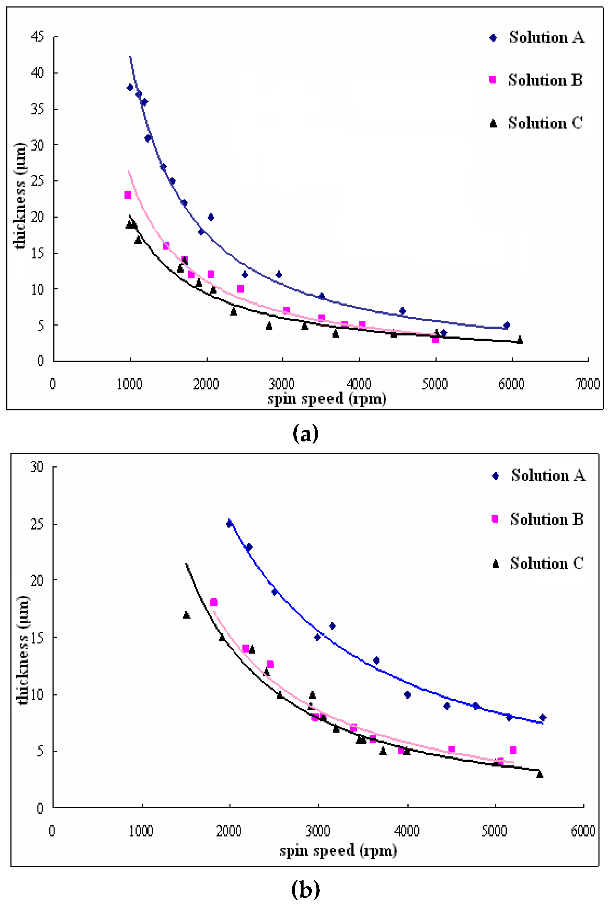
Figure 2a,b shows the relation between spin speed and film thickness for the two considered interfaces; these experimental data were analyzed using nonlinear regression analysis tools. The fitting results are summarized in Table 1. For the three types of prepared solutions, stronger board adhesion yielded thicker films. We first coated the transfer films on the glass boards, and then measured the transfer film thicknesses for different spin speeds. The thicknesses of the fabricated films were measured using an Elcometer 456 coating thickness gauge with an accuracy of ±2.5 μm. The increased toluene volume lowered the solution viscosity. The transfer film thickness decreased as the spin speed increased and the solution viscosity decreased. Figure 2a shows the results for an inactivated glass board, and Figure 2b shows the results for an EVA-pretreated board. The regression analysis results are shown in Figure 2b, where the power regression curve is similar to that shown in Figure 2a, but the thickness is slightly higher. Because the friction force was stronger for the EVA-pretreated board, the resultant transfer film was thicker than that for the inactivated glass board for the same spin speed. The optimal spin speed was 3500 rpm based on the regression analysis, and the goodness-of-fit values (R2) of the fitted models were 0.9758, 0.9715, and 0.9569 for the results in Figure 2a and 0.9807, 0.9518, and 0.9493 for the results in Figure 2b, corresponding to the results for Solution A, Solution B, and Solution C, respectively.
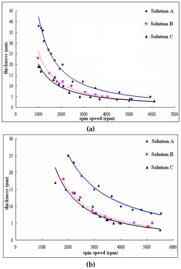
Figure 2.
Relationships between the spin speed and film thickness for different cases. EVA solutions at three concentrations were considered to form the films on two surfaces: (a) inactivated glass board and (b) EVA-coated board. Because the friction force was stronger for the EVA-pretreated board, the corresponding film was thicker than for the inactivated glass board for the same spin speed. Solution A was prepared by dissolving 7 g EVA in 20 mL toluene, Solution B was prepared by dissolving the same amount of EVA in 30 mL toluene, and Solution C was prepared by dissolving the same amount of EVA in 40 mL toluene, as described in “Materials and Methods”. Accuracy of thickness: ±2.5 μm.

Table 1.
Nonlinear regression analysis of film thickness on inactivated glass board and EVA-coated board. X: spin speed in rpm. Y: film thickness in micrometer.
3.2. The Roughness of the Transfer Film
Surface roughness is an important parameter for capturing microdissection, especially when the film thickness is increased, owing to repeated spin coating. If the layers are not sufficiently flat, the film formation will likely fail. Table 2 lists the changes in the overall transfer films’ thickness as the number of coatings increased from 1 to 7; these results are listed for Solutions A, B, and C, and for the spin speed of 3500 rpm. Evidently, the film thickness successfully increased with the treatment with an error of only ±3 μm. The roughness worsened as the coating time increased. Solution A (highest viscosity) caused a severe loss in film flatness when the coating step was repeated three times. The film that was obtained by spin coating using the lower-viscosity EVA solution exhibited a higher flatness. Solution C, with a ratio 7 g of EVA in 40 mL toluene, exhibited better flow viscosity with respect to the film preparation by spin coating. The films were made by repeating the coating step seven times using Solutions B and C, yielding a thickness of 50 μm, which is similar to commercially available films. Lower-viscosity solutions improved surface flatness. With lower-viscosity solutions, thicker films can be obtained by increasing the number of coatings. However, this is time-consuming and causes operational failures and adhesion force loss.
Table 2.
Transfer film thicknesses, for different solutions and different coating numbers. Value represents the average ± standard deviation of 5 measurements. Accuracy of thickness: ±2.5 μm.
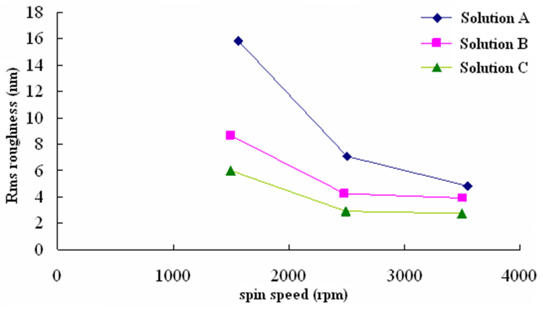
As mentioned above, roughness is an important parameter that determines capture. Figure 3 shows the surface roughness values (parameterized by the root mean squared (RMS)) of the transfer films obtained using different spin speeds and different-viscosity solutions. Increasing the spin speed or decreasing the solution viscosity yielded smoother films. The roughness for Solution C (lowest viscosity) reached 2.762 nm for a spin speed of 3500 rpm. The other two solutions also exhibited better surface states at high spin speeds. Surface flatness did not improve for spin speeds above 3500 rpm. These results suggest that film roughness can be controlled by varying either the spin speed or the solution viscosity. The RMS for the commercially available 50 μm thick film was 4.24 nm. The RMS values for the transfer films obtained using Solution C (thicknesses, 30 μm and 40 μm) were 4.31 nm and 4.75 nm, respectively. Thus, the proposed method is on a par with currently used commercial methods. In the above experiments, the film thickness was measured using a meter, while the RMS and outline figures were obtained using AFM.
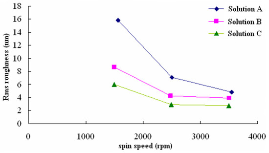
Figure 3.
Film roughness results for different spin speed and viscosity scenarios. Film roughness depends on solution viscosity and spin speed, decreasing with increasing spin speed and/or decreasing viscosity. Film roughness was 2.762 nm for a spin speed of 3500 rpm using Solution C (with lowest viscosity). Roughness was measured using AFM.
3.3. Hot-Melt Dots on the Film
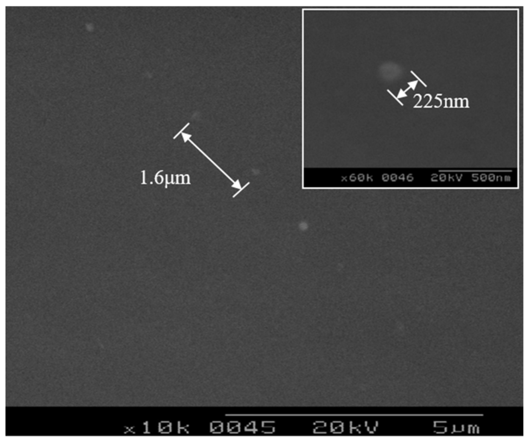
The optimal dye concentration of 0.001 M for the prepared transfer film was determined as described in Section 2.3 “Concentration of the EVA Solution”. After the laser-light irradiation of the film, a regular line composed of light dots was observed using a scanning electron microscope (SEM), as shown in Figure 4. The darker color in the figure represents a lower height, and vice versa. For the dyestuff concentrations of 0.001 M and 0.0015 M, the bright melting dots induced by laser-light irradiation were clear, compared with the surroundings. Furthermore, for the concentration of 0.002 M, the melting dots were not as evident as those for the concentrations of 0.001 M and 0.0015 M. The same was observed in the spectral analysis of the films. The absorbency of the dyestuff did not increase with the increasing concentration. Although the transfer films obtained using the dyestuff concentrations of 0.001 M and 0.0015 M both exhibited the same good hot melt, the concentration of 0.001 M yielded better film transparency. This result indicates that the concentration of the near-infrared light-absorbed dyestuff is better at 0.001 M. Figure 4 shows the hot-melt results for a 30 μm thick transfer film, and the results were obtained using an SEM. The hot-melt dots are regularly distributed along a line on the transfer film. The measured distance between them was 1.6 μm, the same as the displacement associated with driving near the field tip by a piezoelectric ceramic transducer (PZT). The measured dot diameter was 225 nm, far smaller than the resolution of typical conventional LCM (7.5 μm).
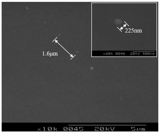
Figure 4.
SEM images of the dots melted by incident laser pulses for a 30 μm thick transfer film. An adequate dye concentration of 0.001 M yielded the optimal thermal energy absorption. The measured dot diameter was 225 nm, as shown in the inset.
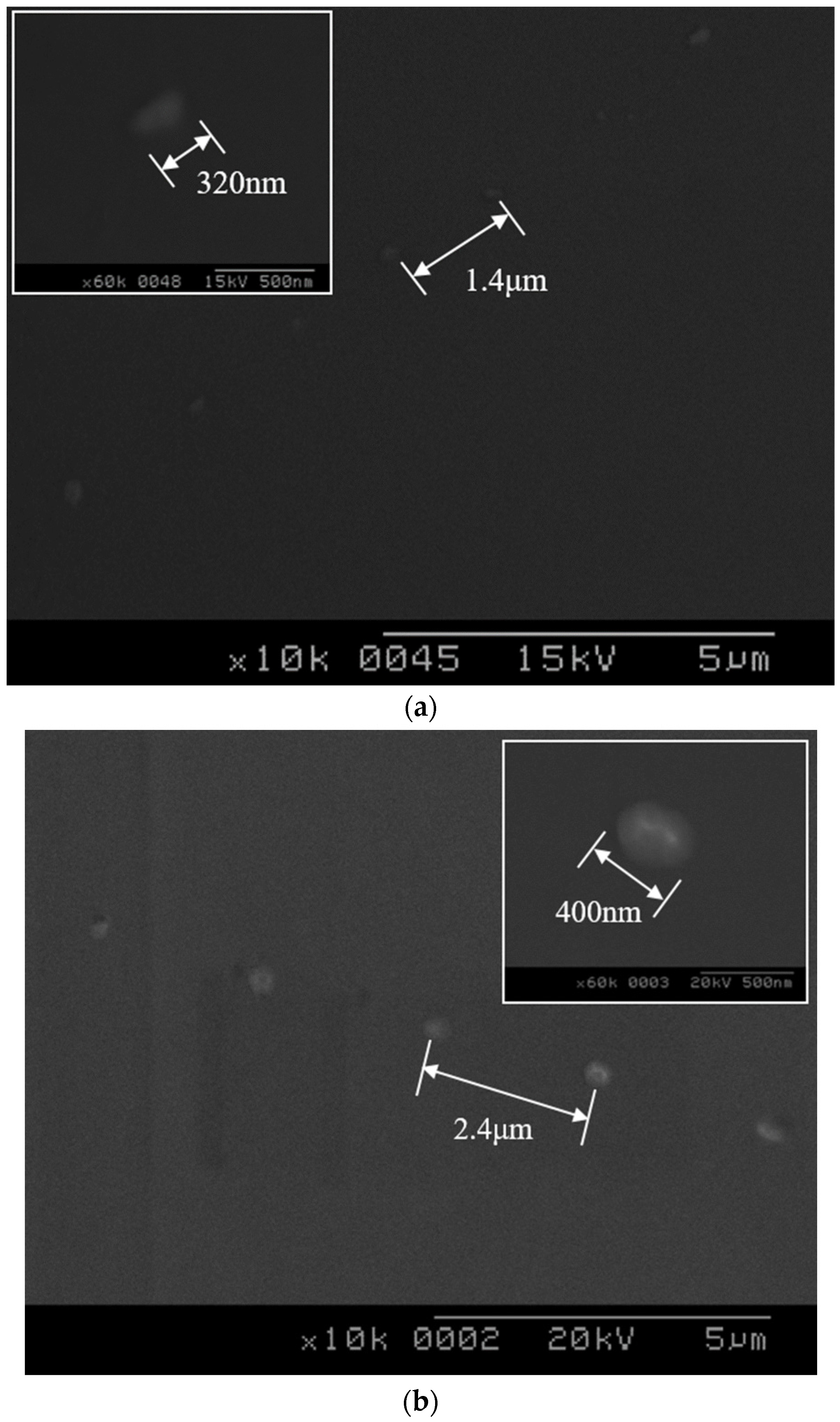
Figure 5a,b shows the results for 39 μm thick and 51 μm thick transfer films, respectively. Evidently, the diameter of the hot-melt dots increased with the increasing film thickness. For the 39 μm thick film, the dot diameter was 320 nm. For the 51 μm thick film, the dot diameter increased to 400 nm, becoming similar to that of the commercially available film. This finding indicates that not only does reducing the distance between the tip and the film improve the dissection resolution, but that film thickness optimization also yields smaller hot-melt zones. Thus, these results suggest venues for resolution improvement. Our results indicate that the thinner the EVA film, the better the film transmittance, and the smaller the number of melt dots, the worse the laser-light absorbance. Although small melt spots improve resolution, poor absorbance may affect the depth of the dip, which in turn may affect capture.

Figure 5.
SEM images of melted dots on different-thickness transfer films. Transfer film thicknesses were (a) 39 μm and (b) 51 μm, while the dots’ diameters were 320 nm and 400 nm, respectively. Inset represents the SEM image taken at 60,000× magnification to show the diameter of melted dot. The effectiveness of the film in (b) was on a par with that of commercially available films.
3.4. Capture of Gold Particles
To determine whether a 30 μm thick film can capture target particles with high resolution, a monolayer of 20 nm diameter gold particles was prepared according to the method of Sato and coworkers [12]. The prepared 30 μm thick film exhibited an effective laser energy absorbance and hot melt.
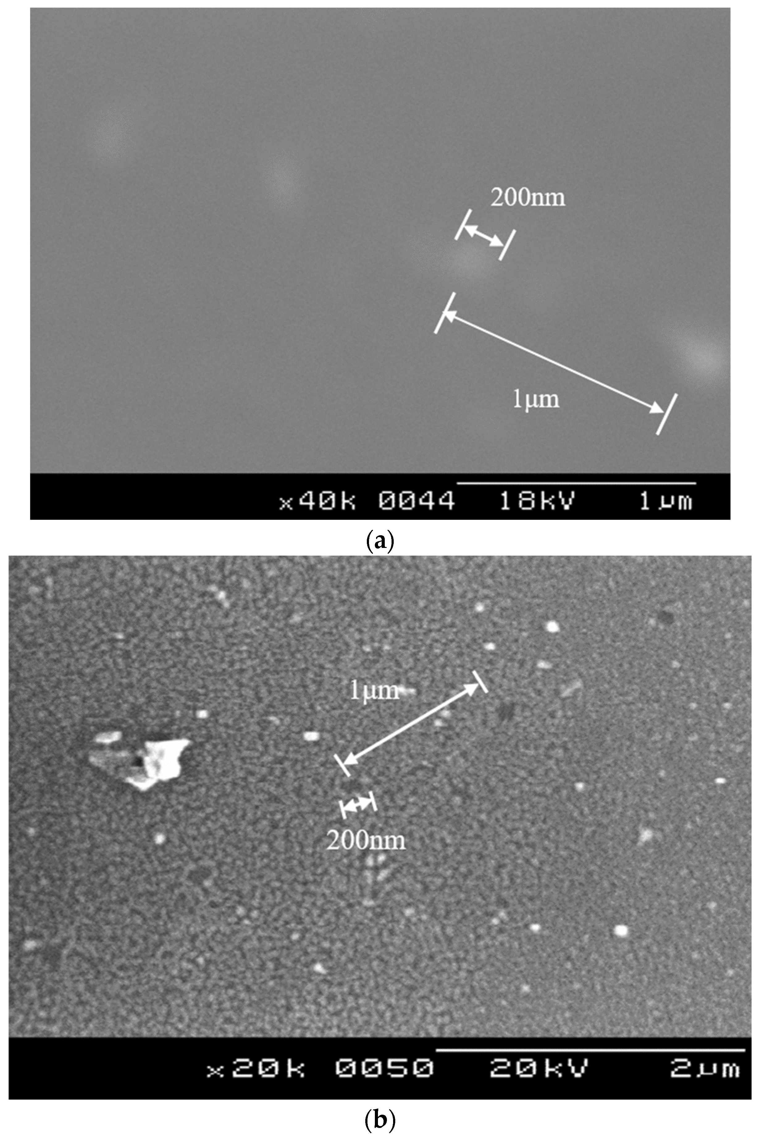
Figure 6a shows an SEM image of the transfer film. In the figure, bright dots are distributed along a line; the distance between adjacent dots is 1 μm, and the approximate dot diameter is 200 nm. Figure 6b shows an SEM image of the monolayer side, with captured trails along a line. The distance between adjacent holes is approximately 1 μm, similar to that for the dots in Figure 6a. The approximate hole size is 200 nm, highly consistent with the sizes of the dots in Figure 6a. This suggests that the transfer film successfully captured the gold particles. Moreover, the capture resolution reached 200 nm when the thickness of the film was 30 μm. For future applications of near-fiber tip LCM systems, the film thickness can be set according to the dissection requirements.
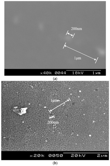
Figure 6.
Laser-based capture of particles for 0.001 M concentration, 30 μm thick transfer films. Particle capture on the 20 nm thick monolayer of gold particles was performed using the prepared transfer film. The diameter of the melted spot on the film was 200 nm, as shown in (a), while the hole size on the monolayer was 200 nm, as shown in (b). Particles with diameters of 200 nm were successfully captured.
4. Conclusions
In this study, an EVA copolymer with an MI value of 400 and a melting temperature of 65 °C was studied, owing to its advantages of high stability, high adhesion ability, and good optical properties. Transfer films were made from an EVA solution containing 7 g of EVA, 40 mL of toluene, and 0.001 M of a near-infrared light-absorbing dye; the films were made using spin coating at a spin speed of 3500 rpm. The transfer films were coated repeatedly, yielding film thicknesses of 30 μm, 40 μm, and 50 μm with corresponding RMS roughness of 4.3 nm, 4.7, nm and 6.1 nm. These roughness values were similar to those of commercially available films (RMS roughness, 4.2 nm). Thinner transfer films yielded smaller melted dots. The capture of 20 nm diameter gold particles with an inter-particle distance of 200 nm was successfully demonstrated using a fabricated 30 nm thick transfer film. Using near-field probe LCM with these thin transfer films, biological samples could be isolated from tissue section more accurately under lower temperature.
Author Contributions
C.-M.C. and C.-F.Y. supervised the study and wrote the manuscript. C.-Y.S. conducted the experiments. C.-M.C., C.-F.Y. and C.-Y.S. performed data interpretation and analysis. All authors edited the manuscript. Project administration, C.-M.C. All authors have read and agreed to the published version of the manuscript.
Funding
This research was funded by the National Science and Technology Council of the Republic of China, grant number 111-2637-E-027-006-.
Institutional Review Board Statement
Not applicable.
Informed Consent Statement
Not applicable.
Data Availability Statement
Not applicable.
Acknowledgments
The authors gratefully appreciate the technical support provided from LOTUN SCIENCE Co., Ltd. and advise from Jen-Ai Lee, Taipei Medical University.
Conflicts of Interest
The authors declare no conflict of interest.
References
- Emmert-Buck, M.R.; Bonner, R.F.; Smith, P.D.; Chuaqui, R.F.; Zhuang, Z.; Goldstein, S.R.; Weiss, R.A.; Liotta, L.A. Laser capture microdissection. Science 1996, 274, 998–1001. [Google Scholar] [CrossRef] [PubMed]
- Banks, R.E.; Dunn, M.J.; Forbes, M.A.; Stanley, A.; Pappin, D.; Naven, T.; Gough, M.; Harnden, P.; Selby, P.J. The potential use of laser capture microdissection to selectively obtain distinct populations of cells for proteomic analysis-preliminary findings. Electrophoresis 1999, 20, 689–700. [Google Scholar] [CrossRef]
- Sirivatanauksorn, Y.; Drury, R.; Crnogorac-Jurcević, T.; Sirivatanauksorn, V.; Lemoine, N.R. Laser-assisted microdissection: Applications in molecular pathology. J. Pathol. 1999, 189, 150–154. [Google Scholar] [CrossRef]
- Suarez-Quian, C.A.; Goldstein, S.R.; Pohida, T.; Smith, P.D.; Peterson, J.I.; Wellner, E.; Ghany, M.; Bonner, R.F. Laser capture microdissection of single cells from complex tissues. Biotechniques 1999, 26, 328–335. [Google Scholar] [CrossRef] [PubMed]
- Stark, R.W.; Rubio-Sierra, F.J.; Thalhammer, S.; Heckl, W.M. Combined nanomanipulation by atomic force microscopy and UV laser ablation for chromosomal dissection. Eur. Biophys. J. 2003, 32, 33–39. [Google Scholar] [CrossRef] [PubMed]
- Chen, C.M.; Lee, J.A.; Yen, C.Y. Improvement in Resolution of Laser Capture Microdissection Using Near-Field Probe to Capture Nanoparticles. IEEE Trans. Nanobioscience 2009, 8, 113–119. [Google Scholar] [CrossRef] [PubMed]
- Chen, C.M.; Shen, C.Y.; Chen, C.Y.; Lee, J.A. The development of a hollow cap thermoplastic film for laser capture micro-dissection with a near field fiber tip. Key Eng. Mater. 2006, 326–328, 731–734. [Google Scholar] [CrossRef]
- Baer, T.M.; Head, D.F.; Toeppen, J.S. Broadband Absorbing Film for Laser Capture Microdissection. U.S. Patent 6,495,195, 2002. [Google Scholar]
- Zaghloul, M.Y.M.; Zaghloul, M.M.Y.; Zaghloul, M.M.Y. Physical analysis and statistical investigation of tensile and fatigue behaviors of glass fiber-reinforced polyester via novel fibers arrangement. J. Compos. Mater. 2023, 57, 147–166. [Google Scholar] [CrossRef]
- Zaghloul, M.M.Y.; Mohamed, Y.S.; El-Gamal, H. Fatigue and tensile behaviors of fiber-reinforced thermosetting composites embedded with nanoparticles. J. Compos. Mater. 2019, 53, 709–718. [Google Scholar] [CrossRef]
- Zaghloul, M.Y.M.; Zaghloul, M.M.Y.; Zaghloul, M.M.Y. Developments in polyester composite materials—An in-depth review on natural fibres and nano fillers. Compos. Struct. 2021, 278, 114698. [Google Scholar] [CrossRef]
- Sato, T.; Hasko, D.G.; Ahmed, H. Nanoscale colloidal particles: Monolayer organization and patterning. J. Vac. Sci. Technol. B Microelectron. Nanometer. Struct. 1997, 15, 45–48. [Google Scholar] [CrossRef]
Disclaimer/Publisher’s Note: The statements, opinions and data contained in all publications are solely those of the individual author(s) and contributor(s) and not of MDPI and/or the editor(s). MDPI and/or the editor(s) disclaim responsibility for any injury to people or property resulting from any ideas, methods, instructions or products referred to in the content. |
© 2023 by the authors. Licensee MDPI, Basel, Switzerland. This article is an open access article distributed under the terms and conditions of the Creative Commons Attribution (CC BY) license (https://creativecommons.org/licenses/by/4.0/).