1. Introduction
At present, the tall buildings in a big city such as Bangkok have been constructed and many more buildings are under construction. In most of those buildings, the walls are made of glass. The glass walls are the major opening parts of the building that absorb the solar radiation and contribute more than 50% of the energy exchange through conduction, convection and radiation [
1,
2]. Therefore, the absorbed solar radiation in the form of heat transfers into the building. This results in the increase of energy consumption by the air conditioners which are generally used in big buildings.
One way to reduce the transmission of infrared radiation into the building is the coating of low-emissivity materials on the glass building [
3]. Low-emissivity coatings display good properties on high reflectance of solar infrared radiation and high visible transmittance. They have been widely used for coating on architectural and automotive flat glass products [
4]. Two types of films were used as low-emissivity coatings for energy saving glasses; metal films and transparent conductive oxide (TCO) films [
5]. The emissivity of metal films is high, but their visible transmittance is low [
5,
6]. The weakness of metal films is poor stability due to the oxidation by the air atmosphere and resulting in the low reflectance of solar infrared radiation [
5]. For TCO film, it is more stable and transparent than those of metal film, but its infrared emissivity is higher [
5,
7]. Among all TCO films, indium tin oxide (ITO) film is the most widely used due to it yielding a low infrared emissivity of about 0.2 [
8,
9]. However, ITO is too expensive for low-emissivity coating on the large-scale glasses.
Therefore, in the past decade, low-emissivity coating methods have been proposed by using the protective layer on both surfaces of metal films. The transparent oxide and sulfide films of various materials including TiO
2, SnO
2, ZnO, ITO and ZnS have been used in a protective layer in dielectric–metal–dielectric multilayer structure [
10]. The low-emissivity coatings of dielectric–metal–dielectric multilayer structure have been widely studied such as TiO
2/Ag/TiO
2, SnO
2/Ag/SnO
2, ZnO/Ag/ZnO, ITO/Ag/ITO and ZnS/Ag/ZnS [
10,
11,
12].
Since the Ag atoms can diffuse through the dielectric layer and react with the oxygen of dielectric layer at high temperature and lead to poor low-emissivity property, chemical durability, corrosion resistance and thermal stability [
13,
14]. A simple method to solve this problem is the coating of a single-layer Ag-based alloy such as Ag–Ti, Ag-Nb and Ag–Ta alloys [
15,
16,
17,
18]. However, those works mainly focus on antibacterial and protective coating applications. Nevertheless, the optical property of Ag-based alloy film as well as the reflectance of NIR radiation of the Ag-based alloy materials still needs to be studied. In addition, alloying with Ta could produce high structure stability [
19].
This work studies a series of Ag–Ta thin films prepared by magnetron co-sputtering on silicon wafer and glass slide substrates. The crystalline structure, surface and cross-sectional morphologies were characterized. The deep investigation on work function and stoichiometric of the Ag–Ta thin Films were investigated by ultraviolet and X-ray photoemission spectroscopies (UPS and XPS), respectively. The reflectance of the Ag–Ta thin films deposited on glass slides at different deposition times were measured by UV–VIS–NIR spectrometer in the wavelength range from 300 to 2000 nm.
2. Experimental Details
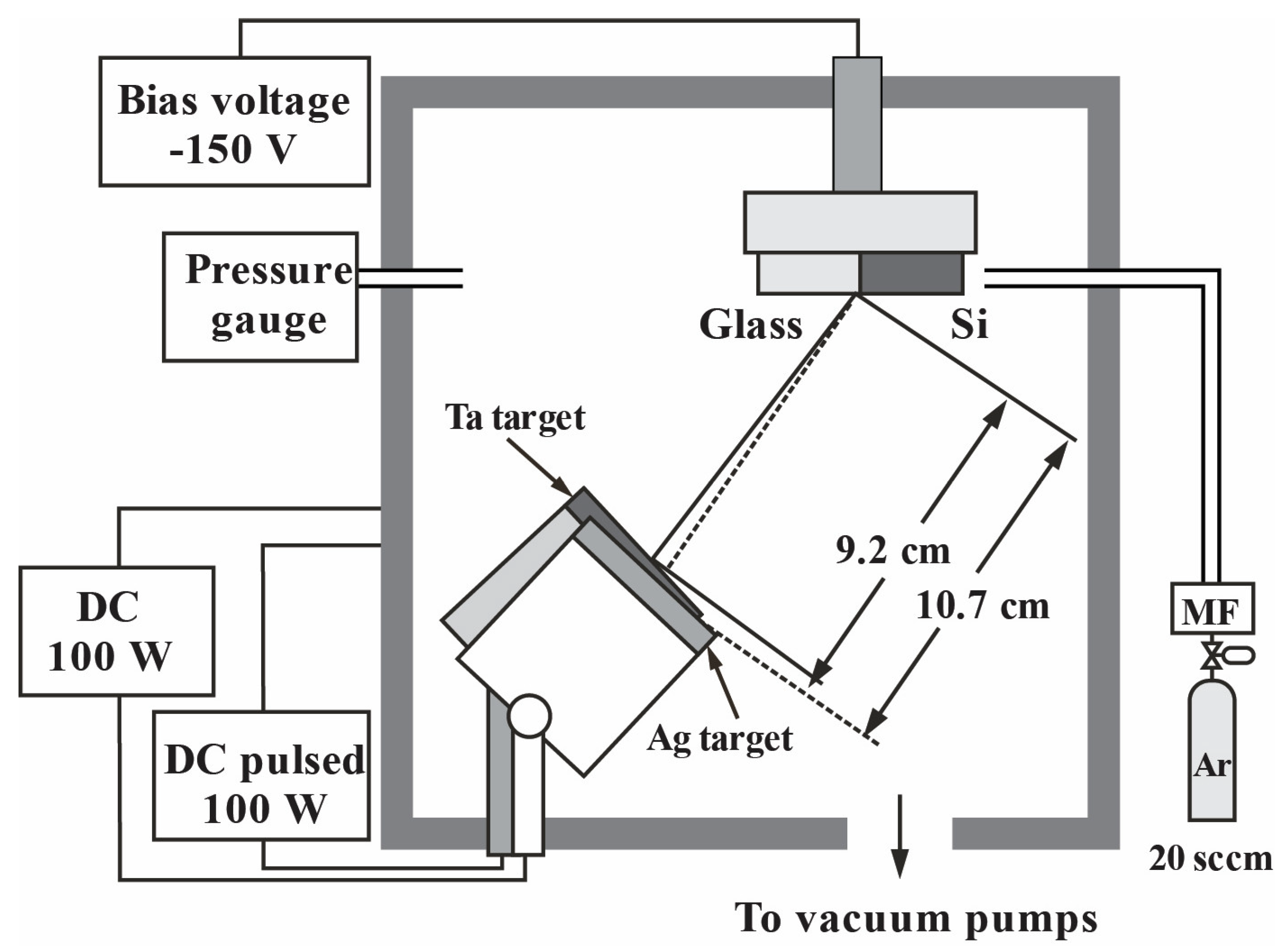
Silver–tantalum (Ag–Ta) thin films were deposited on 1.5 cm × 1.5 cm Si(100) wafers and glass slides, each with a dimension of 2.5 cm × 2.5 cm using a DC magnetron co-sputtering system as shown in
Figure 1. Ag (99.99% purity) and Ta (99.99% purity), each with a diameter of 2 inch and a thickness of 0.25 inch, were used as the targets. The substrates were ultrasonically cleaned in acetone and methanol for 10 min and dried with nitrogen before being installed in the vacuum chamber. The distance from Ag target to substrate (D
s−t(Ag)) and Ta target to substrate (D
s−t(Ta)) were 10.7 and 9.2 cm, respectively.
A home-built vacuum chamber was evacuated to achieve a base pressure of about 3 × 10⁻⁶ Torr by a pumping system consisting of a rotary pump and a diffusion pump. Prior to the deposition, the targets were pre-sputtered with Ar ions for 5 min in order to clear out impure gases in the chamber and to remove the contaminants from the target surface. Then, for sputter-cleaning of the targets, Ar (99.99% purity) was flowed into the chamber with a flow rate of 20 sccm. The Ag target was supplied with a 100 W DC power supply while the Ta target was supplied with a 100 W, 3 kHz DC pulsed power supply. The pressure during deposition was about 5 × 10⁻³ Torr. The films were deposited for various times of 5, 10, 20 and 30 s.
The crystalline structure of Ag–Ta thin films deposited on Si substrates was characterized by a X-ray diffractometer (XRD:Bruker D8 Discover AXS, Billerica, MA, USA) using CuKα radiation (λ = 0.1542 nm) operated at 40 kV and 40 mA. The XRD patterns were recorded at a glancing incidence angle of 2θ with the 2° range from 20° to 80° and a scanning speed of 2°/min. The surface and cross-sectional morphologies of the films deposited on the Si substrates were investigated by a field emission scanning electron microscope (FE-SEM: JEOL, JSM 660 LV, Tokyo, Japan).
The ultraviolet and X-ray photoemission spectroscopy (UPS and XPS) were performed at BL3.2Ua in the Synchrotron Light Research Institute, Nakhon Ratchasima, Thailand. The beamline delivers the soft X-rays ranging from 40 to 1040 eV linearly polarized [
20]. The incident angle is 20 degrees and its polarization is usually parallel to the surface. The CLAM2 electron energy analyzer (Thermo VG Scientific, West Sussex, England) was used to measure the electron energy at an emission angle of 70 degrees. The CLAM2 analyzer was calibrated in the Fermi edge and Au4f7/2 peak at zero and 84 eV, respectively. The samples were loaded into the vacuum chamber and characterized under the pressure of 10–7 Pa at room temperature. The total energy resolutions of UPS and XPS were 0.2 and 2.0 eV, respectively. No changer neutralizer or argon ion etching was applied prior to the measurement. The work function and valence band spectra were measured in the UPS mode at the photon energy of 60 eV on the sample negatively biased at about 10 V. The binding energy is referenced from the Fermi edge of gold. The elemental and chemical compositions of samples were measured in the XPS mode at a photon energy of 600 eV. The binding energy of spectra is referenced from the work function method described elsewhere [
21,
22].
The films deposited on the glass substrates were used for spectral reflectance measurements by a UV–VIS–NIR spectrophotometer (Shimadzu, UV–VIS–NIR 3600, Kyoto, Japan) in the wavelength range from 300 to 2000 nm.
3. Results and Discussion
3.1. Crystal Structure
Figure 2 shows the X-ray diffraction patterns of Ag–Ta thin films deposited on Si substrates with the deposition times of 5, 10, 20 and 30 s. It revealed that the films exhibited preferred orientations of (111) plane for Ag and (110) plane for Ta according to the JCPDS data of the FCC structure of Ag (No. 04-0783) and the BCC structure of Ta (No. 89-5158). It is observed that X-ray intensity of Ag (111) peak is higher than that of Ta (110) peak. This is due to the fact that the atomic number of Ag (47) is lower than that of Ta (73), even though the Ag target was sputtered with 100 W DC supply, whereas Ta target was sputtered with 100 W DC pulsed supply. When the deposition time was increased to 30 s, it revealed that the X-ray intensity of Ag (111) peak and Ta (110) peak increased.
3.2. Surface and Cross-Sectional Morphologies
Figure 3a shows the FE-SEM micrographs of the Ag–Ta films and
Figure 3b shows the cross-sectional FE-SEM images of the Ag–Ta films deposited on Si substrates at various deposition times of 5, 10, 20 and 30 s. From
Figure 3a, the grain size was measured by image-J program and determined to be 4.4, 5.7, 6.8 and 9.5 nm for the deposition times of 5, 10, 20 and 30 s, respectively. From
Figure 3b, the thicknesses for the films deposited at 5, 10, 20 and 30 s were determined to be 7 ± 0.6, 9 ± 0.5, 17 ± 0.9 and 33 ± 1.1 nm, respectively.
3.3. Work Function and Stochiometric
The basic theory related to measuring work function has been reviewed by Helander et al. [
23]. The UPS spectra were measured for the secondary electron cutoff to evaluate the work function of films as shown in
Figure 4a,b. Note that the Fermi level was obtained by gold standard sample. The work function and C1s C–C reference binding energy are listed in
Table 1. The work function of films is ranged from 4.91 to 4.98 eV, which is higher than that of metallic silver and tantalum crystal surfaces. These high work functions tell us that the surface of films is quite flat and uniform [
23]. It might also be due to the formation of alloy film between silver and tantalum.
Figure 5a,b shows the survey XPS spectra and atomic concentration of elements. As shown in
Figure 5a, the secondary electron background increases the baseline of spectra in the low kinetic energy range overlapped with the Auger transitions of C KLL, Ag MNN, and Ta NOO. XPS is sensitive to surface region probed in 3 nm below surface because the inelastic mean free path is short [
24]. Carbon contamination cannot be avoided during the sample transfer from deposition to XPS analysis chamber. Because the films were deposited under the low vacuum condition, the oxidation of films could not be avoided. Atomic concentration of oxygen is ranged from 40 to 50%, and those of other elements are approximately 20% including adventitious carbon at the surface.
Figure 6a–d shows the C1s, O1s, Ta4f, and Ag3d spectra to evaluate the elemental and chemical compositions. The spectral background was removed by the Shieley’s method mixed with polynomial curve in the active background approach [
25]. The peaks were fitted with Gaussian for C1s and O1s spectra at the full width at half maximum (FWHM) of 2 eV. Ta4f peaks were synthesized from Gaussian in the range of FWHM between 1.5 and 3 eV. Ag3d peaks were fitted with the pseudo-Voigt based on the summation of Gaussian (80%) and Lorentzian (20%) at FWHM of about 1.6 eV.
The C1s spectra display the C–C/C–H peak at about 284.6 eV as a major contribution because the carbon originates from the contamination based on the hydrocarbon. Minor contributions of C–O at 1.9 eV below C–C peak and C=O at 3.9 eV below C–C peak were also discovered in the fitting process [
23]. The O1s spectra are derived from three components at 530.5 eV for O
2−, 531.5 eV for O
1−, and 532.7 eV for H
2O [
26]. O
2− content is primarily attributed to the metal oxides with tantalum and silver. O1- content can originate from the O–H/C–O bonds and possibly single metallic bond with tantalum and silver. H
2O content is the highest contribution in TaAg film deposited for 5 s. However, the O
2− content becomes higher than the other contents in the TaAg films deposited for 10–30 s. The Ta4f spectra illustrate two phases of tantalum compositions in the films [
27]. Tantalum oxide (TaO
2, Ta
4+) is identified at the double peaks ranging from 26 to 28 eV. The Ta4f doublet peaks are separated by the spin splitting (1.9 eV) between 7/2 and 5/2, and their amplitudes are constrained at a ratio of 4:3. The other tantalum oxide (Ta
2O, Ta
1+) is also observed from the double peaks from 22 to 24 eV fitted with the same parameters described in tantalum oxide. However, the percentage of Ta
1+ against Ta
4+ is approximately 3–5% at the film surface. The Ag3d spectra appear to be the single phase of metallic silver based on the binding energies of 7/2 peak at 367.7–368.3 eV and 5/2 peak at 373.7–374.3 eV, which are separated by the spin splitting (6.0 eV) and fixed at 3:2 of the amplitude ratio. However, it is difficult to identify the oxidation or chemical state of silver from the peak energy [
28]; no energy loss peak or satellite was determined besides the main peak, so the silver might be partly oxidized or alloyed with tantalum.
3.4. Reflectance Spectra
Figure 7 shows the reflectance spectra of the Ag–Ta thin films deposited on the glass substrates at various deposition times of 5, 10, 20 and 30 s in the wavelength range from 300 to 2000 nm. The spectral reflectance data (R(λ)) were used to calculate the average reflectance in the visible range (λ = 380–780 nm) and near-infrared range (780–2000 nm).
Figure 8 shows the average reflectance in the visible and near-infrared ranges. It can be observed that the film deposited at 30 s can reflect the radiation in the visible range and NIR range by about 60% and 80%, respectively.
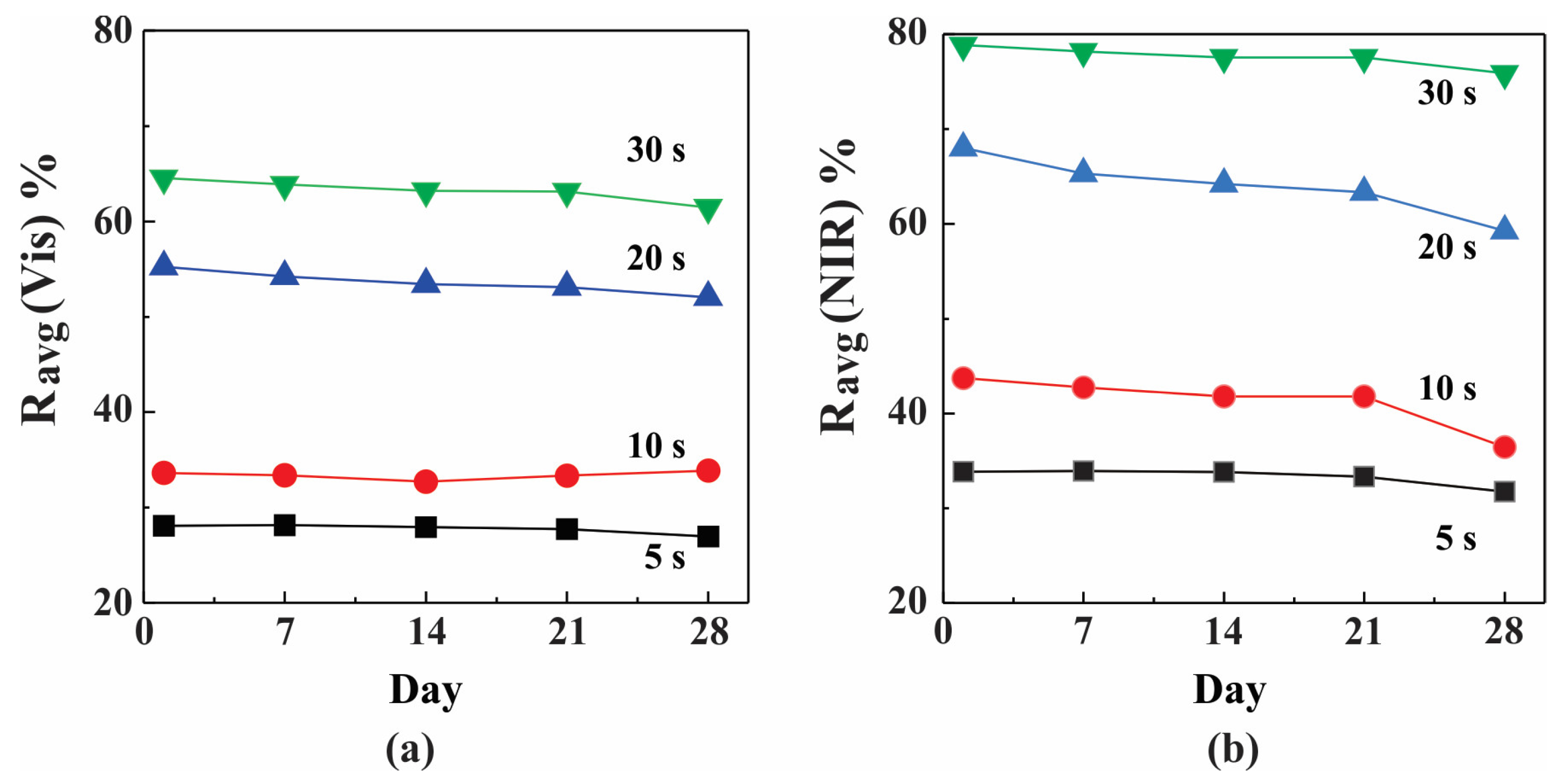
3.5. Durability Test
The durability test of the films deposited on the glass substrates was performed by keeping the samples in the air atmosphere for about one month. The reflection measurements were carried out on the days 7, 14, 21 and 28 and average reflectance in the visible range and NIR were measured, and the results are shown in
Figure 9.
From
Figure 9, it can be observed that the average reflectance for all the films deposited on the glass substrates slightly decreased after being kept in the air atmosphere for 28 days. Furthermore, the film deposited for 30 s has a high average reflectance of more than 75% after being kept in the air for 28 days. The results show that all the films deposited in this work have a good durability, particularly the film deposited for 30 s has an additional property of high NIR reflectance.
4. Conclusions
In this work, single-layer Ag–Ta thin films were deposited on the glass and Si (100) substrates using co-sputtering method for high reflection of NIR radiation. Ag and Ta were used as sputtering targets. The Ag and Ta targets were supplied by a 100 W DC power supply and a 100 W DC pulsed power supply, respectively. The films were deposited at various times of 5, 10, 20 and 30 s.
The thicknesses of the films deposited at 5, 10, 20 and 30 s, as determined from the cross-sectional FE-SEM images, were determined to be 7.16, 9.81, 17.43 and 33.93 nm, respectively. The reflectance spectra showed that the film deposited at 30 s had an average reflectance of about 80% in the NIR range and it decreased to 75% after the films were kept in the air atmosphere for 28 days. The atomic concentration of elements of Ag–Ta films as investigated by XPS showed that the concentrations of Ag, Ta, O2 and C were determined to be about 20, 20, 40 and 20%, respectively, in all prepared films. This means that Ag and Ta oxide films were formed during the deposition or the waiting time for characterization in which this problem is unavoidable. For the overall result, it can be concluded that the Ag–Ta thin films prepared in this work are acceptable for high NIR reflection. They can be coated on the glass building for saving energy in the building.
Author Contributions
Conceptualization, W.P.-N. and M.H.; methodology, N.T. and C.C.; validation, H.N., N.T. and C.C.; formal analysis, W.P.-N. and S.K.; investigation, K.K. and W.H.; resources, W.H.; data curation, K.K., S.K. and W.H.; writing—original draft preparation, S.K.; writing—review and editing, S.K.; supervision, W.P.-N.; project administration, W.P.-N. and S.K.; funding acquisition, W.P.-N., T.R. and M.H. All authors have read and agreed to the published version of the manuscript.
Funding
This research was funded by Biodiversity-Based Economy Development Office (Public Organization), Grant No. BEDO-NRCT 47/2562.
Institutional Review Board Statement
Not applicable.
Informed Consent Statement
Not applicable.
Data Availability Statement
Not applicable.
Acknowledgments
This research work was supported by Phranakhon Rajabhat University and Biodiversity-Based Economy Development Office (Public Organization). The authors would like to thank National Electrics and Computer Technology Center for providing the deposition system and spectrophotometer.
Conflicts of Interest
The authors declare no conflict of interest.
References
- Su, J.; Yin, L.; Qin, L.; Ma, N.; Huang, J. Preparation and performance of ZrAlN antireflective coatings for low-emissivity glasses. Ceram. Int. 2017, 43, 14616–14622. [Google Scholar] [CrossRef]
- Kumar, G.K.; Saboor, S.; Babu, T.P.A. Investigation of various low emissivity glass materials for green energy building construction in indian climatic zones. Mater. Today Proc. 2017, 4, 8052–8058. [Google Scholar] [CrossRef]
- Gläser, H.J.; Ulrich, S. Condensation on the outdoor surface of window glazing calculation methods, key parameters and prevention with low-emissivity coatings. Thin Solid Film. 2013, 532, 127–131. [Google Scholar] [CrossRef]
- Park, S.H.; Lee, K.S.; Reddy, A.S. Low emissivity Ag/Ta/Glass multilayer thin films deposited by sputtering. J. Appl. Phys. 2011, 110, 063501–063508. [Google Scholar] [CrossRef]
- Sun, K.; Tang, X.; Yang, C.; Jin, D. Preparation and performance of low-emissivity Al-Doped ZnO films for energy-saving glass. Ceram. Int. 2018, 44, 19597–19602. [Google Scholar] [CrossRef]
- Loka, C.; Yu, H.T.; Lee, K.S. The preparation of thermally stable TiNx/Ag(Mo)/TiNx ultrathin films by magnetron sputtering. Thin Solid Film. 2014, 570, 178–182. [Google Scholar] [CrossRef]
- Giovannetti, F.; Föste, S.; Ehrmann, N.; Rockendorf, G. High transmittance, low emissivity glass covers for flat plate collectors: Applications and performance. Energy Procedia 2012, 30, 106–115. [Google Scholar] [CrossRef][Green Version]
- Sibin, K.P.; Swain, N.; Chowdhury, P.; Dey, A.; Sridhara, N.; Shashikala, H.D.; Sharma, A.K.; Barshilia, H.C. Optical and electrical properties of ITO thin films sputtered on flexible FEP substrate as passive thermal control system for space applications. Sol. Energy Mater. Sol. Cells 2016, 145, 314–322. [Google Scholar] [CrossRef]
- Shi, Z.; Song, L.; Zhang, T. Terahertz reflection and visible light transmission of ITO films affected by annealing temperature and applied in metamaterial absorber. Vacuum 2018, 149, 12–18. [Google Scholar] [CrossRef]
- Chiba, K.; Kaminishi, S. Fabrication and optical properties of low-emissivity coatings of AlSiN and AgCuNd-Alloy multilayer films on glass. Jpn. J. Appl. Phys. 2008, 47, 240–243. [Google Scholar] [CrossRef]
- Dhar, A.; Alford, T.L. High quality transparent TiO2/Ag/TiO2 composite electrode films deposited on flexible substrate at room temperature by sputtering. APL Mater. 2013, 1, 12102–12107. [Google Scholar] [CrossRef]
- Kim, J.H.; Kim, D.H.; Kim, S.K.; Bae, D.; Yoo, Y.Z.; Seong, T.Y. Control of refractive index by annealing to achieve high figure of merit for TiO2/Ag/TiO2 multilayer films. Ceram. Int. 2016, 42, 14071–14076. [Google Scholar] [CrossRef]
- Kulczyk-Malecka, J.; Kelly West, P.J.G.; Clarke, G.C.B.; Ridealgh, J.A.; Almtoft, K.P.; Greer, A.L.; Barber, Z.H. Investigation of silver diffusion in TiO2/Ag/TiO2 coatings. Acta Mater. 2014, 66, 396–404. [Google Scholar] [CrossRef]
- Loka, C.; Yu, H.T.; Lee, K.S. Effect of TiNx Inter/Outer layer on Ag(Cr) thin films at elevated temperatures for low emissivity applications. Jpn. J. Appl. Phys. 2014, 53, 3014–3017. [Google Scholar] [CrossRef]
- Kao, K.S.; Cheng, D.L.; Chang, S.H.; Hsieh, P.T.; Chin, H.S.; Lin, H.K. Effect of mesh fatterning with UV pulsed-laser on optical and electrical properties of ZnO/Ag–Ti thin Films. Appl. Surf. Sci. 2010, 256, 7446–7450. [Google Scholar] [CrossRef]
- Wojcieszak, D.; Mazur, M.; Kaczmarek, D.; Mazur, P.; Szponar, B.; Domaradzki, J.; Kepinski, L. Influence of the surface properties on bactericidal and fungicidal activity of magnetron sputtered Ti–Ag and Nb–Ag thin films. Mater. Sci. Eng. C 2016, 62, 86–95. [Google Scholar] [CrossRef]
- Wang, J.; Li, J.; Li, H.; Zhang, X.; Huang, J.; Xiong, D. Friction and wear properties of amorphous and nanocrystalline Ta-Ag films at elevated temperatures as function of working pressure. Surf. Coat. Technol. 2018, 353, 135–147. [Google Scholar] [CrossRef]
- Jianliang, L.; Jun, W.; Ameet, K.; Hang, L.; Dangsheng, X. High temperatures tribological properties of Ta-Ag films deposited at various working pressures and sputtering powers. Surf. Coat. Technol. 2018, 349, 186–197. [Google Scholar] [CrossRef]
- Jianliang, L.; Xiafei, Z.; Jun, W.; Hang, L.; Jiewen, H.; Heguo, Z.; Dangsheng, X. Mechanical and frictional performance of Ta and Ta-Ag alloy films deposited at different sputtering powers. J. Mater. Eng. Perform. 2019, 28, 5037–5046. [Google Scholar] [CrossRef]
- Hideki, N.; Sarunyu, C.; Porntip, S.; Surachet, R.; Watcharapon, J.; Ratchadaporn, S.; Narong, C.; Prayoon, S. Commissioning of the soft X-Ray undulator beamline at the siam photon laboratory. In Proceedings of the 12th International Conference on Synchrotron Radiation Instrumentation SRI2015, New York, NY, USA, 6–10 July 2015; AIP Publishing: Melville, NY, USA, 2016; Volume 1741, pp. 020040-1–020040-4. [Google Scholar] [CrossRef]
- Greczynski, G.; Hultman, L. X-ray photoelectron spectroscopy: Towards reliable binding energy referencing. Prog. Mater. Sci. 2019, 107, 100591. [Google Scholar] [CrossRef]
- Greczynski, G.; Hultman, L. C 1s peak of adventitious carbon aligns to the vacuum level: Dire consequences for material’s bonding assignment by photoelectron spectroscopy. ChemPhysChem 2017, 18, 1507–1512. [Google Scholar] [CrossRef] [PubMed]
- Helander, M.G.; Greiner, M.T.; Wang, Z.B.; Lu, Z.H. Pitfalls in measuring work function using photoelectron spectroscopy. Appl. Surf. Sci. 2010, 256, 2602–2605. [Google Scholar] [CrossRef]
- Powell, C.J.; Jablonski, A. Surface sensitivity of X-ray photoelectron spectroscopy. Nucl. Instrum. Methods Phys. Res. A 2009, 601, 54–65. [Google Scholar] [CrossRef]
- Engelhard, M.H.; Baer, D.R.; Herrera-Gomez, A.; Sherwood Peter, M.A. Introductory guide to backgrounds in XPS spectra and their impact on determining peak intensities. J. Vac. Sci. Technol. A 2020, 38, 063203–063224. [Google Scholar] [CrossRef]
- Jean-Charles, D.; Danielle, G.; Philippe, V.; Alain, L. Systematic XPS studies of metal oxides, hydroxides and peroxides. Phys. Chem. Chem. Phys. 2000, 2, 1319–1324. [Google Scholar] [CrossRef]
- Robin, S.; Richard, W.; John, W.; Mark, B. XPS investigation of monatomic and cluster argon ion sputtering of tantalum pentoxide. Appl. Surf. Sci. 2017, 405, 79–87. [Google Scholar] [CrossRef]
- Maria, A.; Ferraria Patrícia Carapeto, A.; Maria Botelho do Rego, A. X-ray photoelectron spectroscopy: Silver salts revisited. Vacuum 2012, 86, 1988–1991. [Google Scholar] [CrossRef]
| Disclaimer/Publisher’s Note: The statements, opinions and data contained in all publications are solely those of the individual author(s) and contributor(s) and not of MDPI and/or the editor(s). MDPI and/or the editor(s) disclaim responsibility for any injury to people or property resulting from any ideas, methods, instructions or products referred to in the content. |
© 2022 by the authors. Licensee MDPI, Basel, Switzerland. This article is an open access article distributed under the terms and conditions of the Creative Commons Attribution (CC BY) license (https://creativecommons.org/licenses/by/4.0/).


 ,
, 


