1. Introduction
Optically transparent and ultra-thin films are essential for the production of liquid crystal displays, solar cells, various sensors, medical devices, etc. Indium-tin-oxide (ITO) coatings are often used for the manufacture of these devices due to their high optical transparency (in the visible light spectrum) and electrical conductivity [
1,
2,
3,
4]. These thin layers also have good resistance to environmental influences (e.g., humidity and ambient temperature fluctuations).
For this reason, ITO coatings are often used to manufacture heating elements for car windshields and rear windows as an optically transparent thin-layer heating element can be formed. As the conditions of the environment change, ITO film parameters such as the optical transparency and electrical conductivity remain constant for a long time. This feature is important to ensure stable operation at various (e.g., various sensors, organic photovoltaics and liquid crystal displays) outdoor conditions [
1,
2,
3,
5,
6]. Researchers demonstrated that the mesoporous ITO could be used as a photocathode material in p-type dye-sensitized solar cells [
7].
The following technological problems are encountered in the growth of various nano-size films and in the formation of flexible surfaces: many flexible optical materials have low heat performance limits (up to 350 °C), and materials, such as polyethylene terephthalate (PET), polycarbonate (PC), polymethyl methacrylate (PMMA) and polystyrene (PS), have difficulty withstanding the temperature of the crystallization process [
1,
8]. For this reason, low-temperature film-forming processes (up to 300 °C) are the most commonly used [
4,
8,
9].
In the formation of ITO thin films and their heat treatment problems (such as the different coefficients of the thermal expansion of different layers) are encountered. As a result, various stresses and microdefects occur that reduces the technological properties of ITO films and their adhesion to various surfaces [
10,
11]. Various solutions have been proposed to solve this problem, e.g., the formation of a dense grid of ITO thin-layer structures on various flexible surfaces [
1,
2].
Various technologies are used to synthesize and manufacture ITO films, such as spin-coating [
12], magnetron sputtering [
8,
9,
10], reactive thermal evaporation [
13], sol–gel [
14], electron beam gun [
11] and pulsed laser deposition [
15,
16]. Traditionally, the formation and annealing of ITO layers takes place at 150 and 180 °C. However, annealing temperatures of up to 900 °C could be used to improve the optical and electrical properties of formed ITO films. The purpose of annealing is to have an optical transmittance of at least 80% [
10,
11,
14]. It should be noted that the amorphous phase of ITO films is converted into a polycrystalline state by annealing [
11].
Use of pulsed laser deposition or combined deposition methods with annealing for the formation and processing of ITO films is relatively slow or costly [
13,
14,
15,
16]. Various alternatives are being sought to accelerate the technological processes of ITO film synthesis. Such alternatives include various plasma technologies that can be used to deposit ITO thin films for various technological applications [
4,
8,
9,
10,
17]. However, it should be noted that the microstructure and properties of thin ITO films is highly dependent on the deposition process conditions, such as the pressure of the plasma-forming gas, the duration of the deposition process, the substrate temperature and type of plasma gases [
8,
9,
10,
17,
18].
Researchers demonstrated that the optical and electrical properties of the ITO films are strongly related to the formation parameters and technology used for the deposition. H. Zhang et al. [
19] indicated that the transmittance in visible light range and the band gap (from 3.31 to 3.81 eV) of the ITO films increased with the increase of sputtering power. H. Zhu et al. [
10] obtained that the resistivity and transmittance of ITO films were reduced with the increase of annealing temperature.
L. Wen et al. [
17] demonstrated that the increase of oxygen flow rate reduced the band gap values of ITO films. Y. Ren et al. [
14] indicated that the annealing temperature affects the chemical composition, and due to this the optical and electrical properties of ITO films can be controlled. C.S. Belo et al. [
13] showed that the optical and electrical properties of ITO films depended on the oxygen partial pressures when the reactive thermal evaporation was used.
J.L. Chiang et al. [
8] obtained the resistance of 350–500 Ω/sq, resistivity of ~10 Ω and light transmittance of 88% in the visible range of ITO films by managing the magnetron sputtering parameters. The doping of the ITO films with metals was also used to improve the electrical and optical properties [
9,
20]. Y.T. Li et al. [
9] found that Zr-doped ITO films demonstrated higher transmittance values compared to undoped ones. The addition of low concentration (up to 2 wt.%) cerium reduced the surface roughness, increased the density, transparency and electrical conductivity of the ITO films [
20].
The formation of ITO films directly on the heated substrates increased the efficiency and cost of the manufacturing process and enhanced the quality of the formed films. The produced ITO films contained lower amount of defects, higher crystallization degrees, etc. [
4,
8,
9,
21]. However, the information on the application of plasma-activated reactive evaporation technology for the formation of ITO films is limited.
As the final properties of ITO films strongly depend on the elemental composition, formation temperature, gas type, elemental composition, etc., it is important to determine the optimal substrate temperature, initial tin and indium mass ratio, etc. in order to produce ITO films with a high optical transparency and the required electrical properties. The aim of this work was to grow indium-tin oxide thin films on heated substrates by plasma-activated reactive thermal evaporation and to study their optical and electrical properties. The characteristics of the ITO films with optimal optical and electrical properties for defrosting and heating icy windows application were investigated.
2. Materials and Methods
Thin films of indium-tin oxide were evaporated on glass substrates (Superior Marienfeld company microscope slides, Lauda-Königshofen, Germany). The deposition was performed using plasma-activated reactive evaporation technology [
22]. For this purpose, an oxygen flow meter is connected to the chamber, which allows changing the oxygen gas flow from 0 to 500 cm
3/min. Plasma is generated between the screen and the sample holder using a high voltage direct current source. The evaporation of material is performed from a molybdenum bed by adding the desired amount of indium and tin material to it. By varying the mass ratios of indium and tin for evaporation, the coatings of different elemental compositions are obtained.
The maximum vacuum that can be achieved with this system is 5–10
−3 Pa. The deposition of ITO films was performed at an oxygen gas pressure of 4 Pa, the distance between glass substrates and evaporation boat was 0.10 m, the discharge current was 0.625 A, the voltage (between the screen and sample) was kept at 400 V, and the current (through the evaporator) was 75 A. ITO films were deposited using various mass ratios of indium and tin (
Table 1). During the deposition, the temperature of all glass substrates was 350 °C. Higher substrate temperatures improve the adhesion between the layer and the substrate and increase the energy of the atoms and their mobility on the substrate surface.
This temperature was chosen because the tin impurities would be “activated” during the growth of the coating, tin atoms would have enough energy to replace the indium atoms in the nodes of the crystal lattice and thus increase the number of free electrons in the conduction band. The weight of the evaporated material was determined on an A&D GR 202 analytical balance, A&D Company, Limited, Tokyo, Japan. The absolute error of the balance was 0.01 mg. The thickness of the grown ITO coatings was measured with a stylus profiler (Ambios XP-200, Ambios Technology Inc., Santa Cruz, CA, USA). The results indicated that the thickness of the evaporated ITO films varied in the range of 755–800 nm (
Table 1).
The surface resistances of the ITO films were measured using the four-probe method. Current is passed through the edge probes and the potential difference between the middle probes is measured. The surface resistivity of a film when a thickness is significantly less than its width, and the length is calculated using the equation:
where
Rs is the film resistance (expressed in Ω/sq.),
U is the voltage drop measured across the inner probes and
I is the current applied at the outer probes.
The resistivity (
) of the deposited ITO films was calculated using the following equation:
where
d is the thickness of the ITO films.
The electrical and electro-thermal properties of indium-tin oxide were determined by applying a constant voltage to the contacts of the sample and measuring the strength of the electric current flowing through the layer. Thus, the volt-ampere dependencies of the layer and the contacts were determined. The surface temperature of the layer was measured by a K-type thermocouple. The transmittance spectra of the ITO films were measured at normal incidence with a UV–VIS–NIR spectrophotometer (Ocean Optics USB4000, Ocean Optics, Inc., Dunedin, FL, USA) at the 350–850 nm range.
The coating structure was analysed by X-ray diffraction (XRD) (DRON-UM1 with standard Bragg-Brentano focusing geometry, Bourevestnik, JSC, Saint-Petersburg, Russia) in a range of 10°–100° applying the CuKα (λ = 0.154059 nm) radiation. The scanning electron microscope (RAITH-e-LiNE, Raith GmbH, Dortmund, Germany) was employed to analyse the morphology of the produced coatings (working distance—8.6 mm, accelerating voltage—10 kV).
The elemental composition of the coatings was estimated using the energy dispersive X-ray spectroscopy (EDS) (Bruker AXS from GmbH, Bruker corporation, Billerica, MA, USA). Equipment used for these studies: power supply (AIM-TTI INSTRUMENTS, PL303QMD, Aim and Thurlby Thandar Instruments, Cambridgeshire, UK), which changes the voltage from 0 to 30 V, ammeter (Agilent 34410A, Agilent Technologies, Santa Clara, CA, USA), multimeter (Mastech MS 8229, Mastech Group, Charlotte, NC, USA) with a thermoporous probe. Measurements at lower temperatures were performed by freezing the sample in a Peltier element, and the sample temperature was lowered down to −10 °C.
3. Results and Discussion
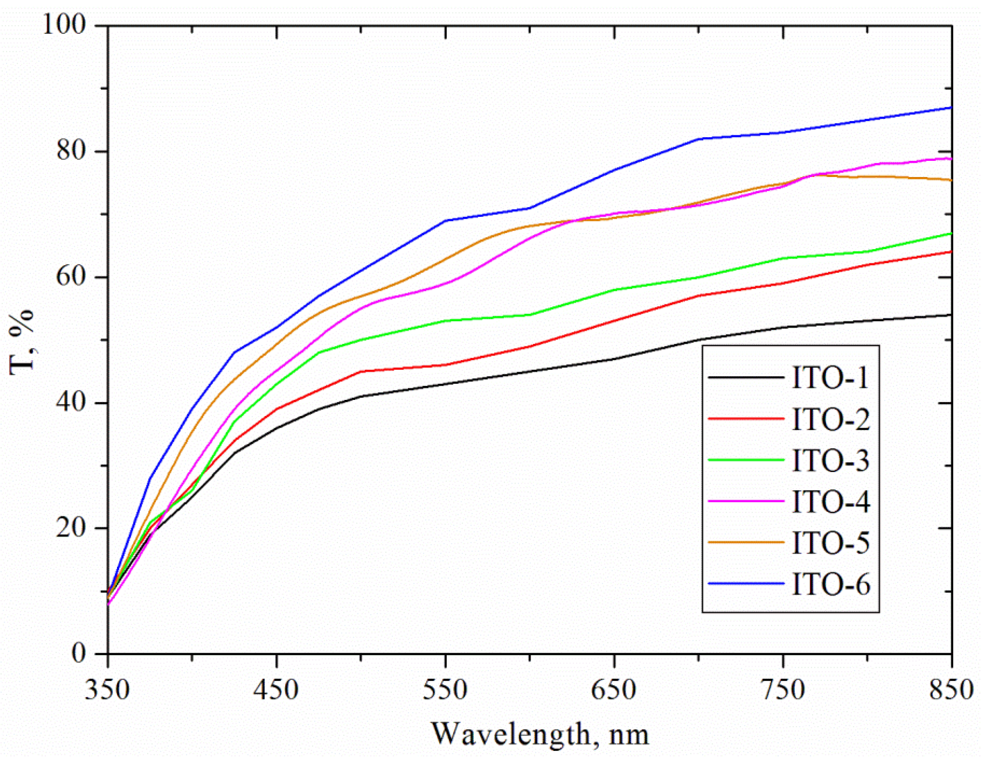
The optical characteristics of the ITO films deposited using various indium and tin mass ratios in the range of 350–850 nm are shown in
Figure 1 and
Figure 2. As it can be seen, the optical transmittance of the coatings was found to increase with increasing the wavelength from 350 up to 850 nm (
Figure 1). The ITO-1 film deposited using the highest amount of tin demonstrated the lowest transmittance values of 10% and 50% at 350 and 850 nm wavelengths, respectively.
The increase of the MIn/MSn ratio from 4.25 to 6.00 increased the transmittance values by 10% in visible light region. The highest transmittance values were obtained for the ITO-6 film and varied from 50% to 90% with the increase of wavelength from 400 to 850 nm. The results indicated that the transmittance values was enhanced when the MIn/MSn ratio increased from 4.25 (ITO-1) up to 10.00 (ITO-6).
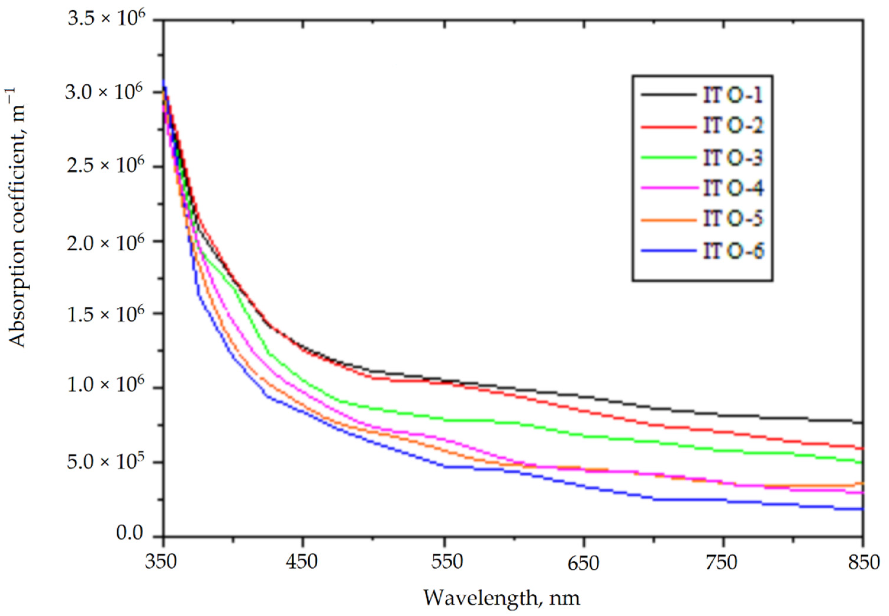
In order to compare the optical properties of ITO films with slightly different layer thicknesses, it is necessary to calculate a linear absorption coefficient. The dependence of ITO coatings absorption coefficients on the wavelength is shown in
Figure 2. We obtained that the absorption coefficient of ITO films was reduced when the M
In/M
Sn ratio increased from 4.53 (ITO-1) to 10.00 (ITO-6). Thus, the ITO films deposited using a lower amount of tin demonstrated higher absorption coefficient values in visible wavelength range.
The average values of optical transmittance at the wavelengths of 400–760 nm were calculated (
Figure 3). The lowest transmittance value (~43%) was for the ITO film prepared with the highest tin amount. As the M
In/M
Sn ratio increased from 4.25 to 6.00, the transmittance enhanced from 43% to 51%, respectively. The transmittance of the as-deposited ITO films enhanced from 51% to ~59% in the visible wavelength range when the M
In/M
Sn ratio increased from 6.00 to 7.4. The further increase in the M
In/M
Sn ratio led to only a slight increase of transmittance values of ITO films from ~61% to ~64%.
The energy gap values of deposited ITO films can be calculated using the Tauc relation [
10,
11] as follows:
where α is the light absorption index, h is the Planck constant, v is the frequency, A indicates an independent parameter of photon energy, E
g is the optical band gap, and the index
n identifies the type of the transition in the material.
Various authors [
10,
11,
23] recommended different
n index values: for direct bandgap (crystalline semiconductors) material and for indirect bandgap (amorphous semiconductors) material
n = 1/2 and
n = 2, respectively. The graphs of the relationship between (α × h × v)
2 and hv for all ITO films were calculated by Equation (3), and the optical bandgap values were determined by extrapolating the linear portion of the curve to (α × h × v) = 0. The bandgap of films at different M
In/M
Sn mass ratios is given in
Figure 3.
As it can be seen, the bandgap of deposited ITO films increased from 3.18 to 3.37 eV, as the M
In/M
Sn ratio was enhanced from 4.25 to 10.00. The increase in bandgap from 3.18 to 3.37 eV is related to increase in carrier concentration of ITO films [
23]. The dependence of resistivity and resistance of ITO films on the M
In/M
Sn mass ratio are presented in
Figure 4. The resistance of ITO films enhanced from 92 up to 560 Ω/sq, when the M
In/M
Sn mass ratio increased. The resistivity of the deposited ITO films enhanced from 7.4 × 10
−3 to 43.7 × 10
−3 Ω·cm, as the M
In/M
Sn ratio changed from 4.25 to 10.00. It should be noted that the reduction of the tin content during the deposition of ITO films increased the transparency and resistivity values.
Conductivity of ITO films improves with the increase of the carrier density [
14]. One method to increase the carrier density in ITO films is to create additional oxygen vacancies. The oxygen vacancy can release two weakly bound electrons, which become carriers involved in conduction. Simultaneously, the decrease of adsorbed oxygen can improve the Hall mobility and release some carriers bound with adsorbed oxygen [
14,
19]. Y.T. Li et al. [
9] indicated that the increase of the bandgap of Zr doped ITO films is directly related to the reduction of carrier concentrations from 6.38 × 10
19 to 4.90 × 10
19 cm
3.
Research demonstrated that the increase in the grain boundaries reduced the carrier mobility. However, the mobility of the carriers was enhanced when the denser crystal grains were formed [
19]. The electrical properties of ITO films strongly depend on various deposition parameters. The resistance values of ITO films vary from 6 up to 1 × 10
5 Ω/sq. The resistivity of ITO films changes from 3 × 10
−4 to 120 × 10
−3 Ω·cm [
8,
24,
25]. L. Wen et al. [
17] observed that the variation of In/Sn atomic ratio affects the optical band gap, transmittance and resistivity values of ITO films.
B.R. Cho et al. [
21] observed that the sheet resistance of ITO films decreased with the increase of the substrate temperature. The possibility of tin atoms to migrate into the indium oxide lattice as interstices enhances with an increase in the temperature of the substrate [
10,
21]. The post-annealing of the ITO films after the deposition also reduces the sheet resistance values [
10,
11,
21]. The higher temperature supplies an additional energy to atoms and stipulates the migration of deposited atoms. As a result, this reduces the defect state density and improves the crystallization of the ITO films [
10].
The optical and electrical measurements of the formed ITO films indicated that the initial MIn/MSn mass ratio has a huge effect. Thus, the ITO-5 film deposited at the MIn/MSn ratio of 9.25 was chosen for detailed studies as it demonstrated the optimal combination of the optical (high transmittance and bandgap) and electrical properties.
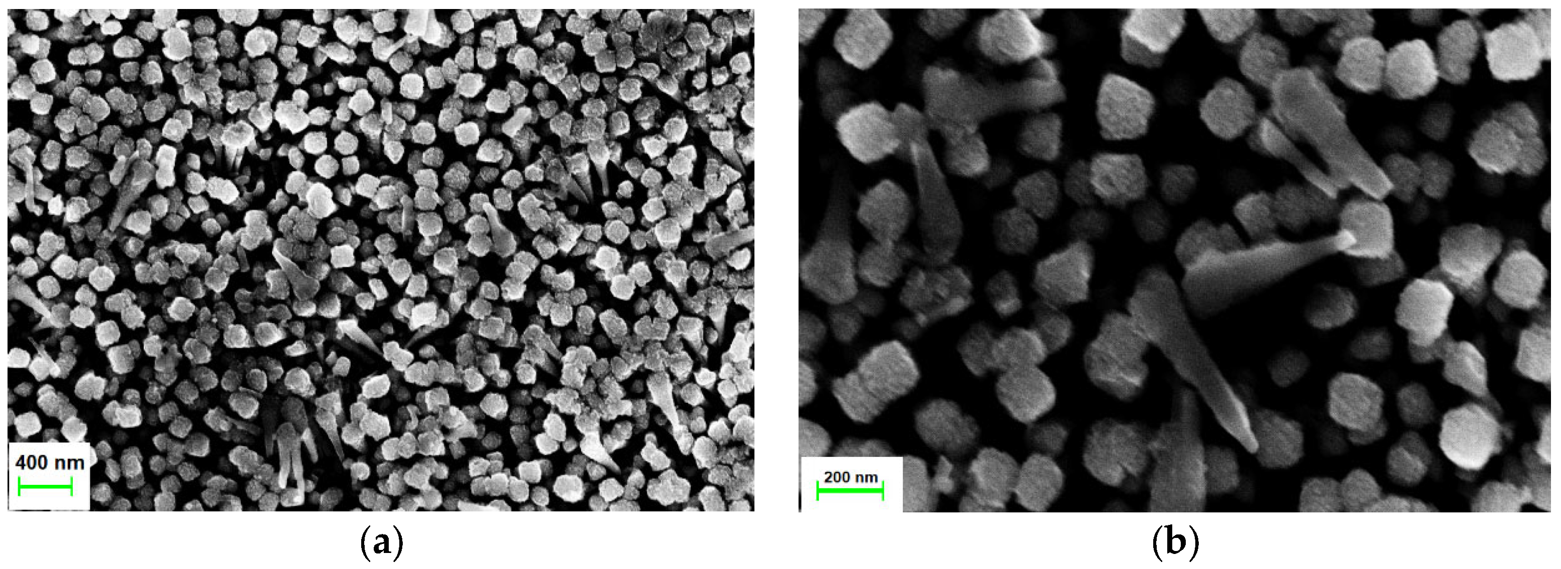
Surface morphology images of ITO-5 film are shown in
Figure 5. An even larger magnification (50,000) of the same coating surface is shown in
Figure 5b. Surface views show that the layer grows in relatively sparse columns perpendicular to the substrate with a diameter from 100 to 150 nm. The shape of the grains is cubic-like. The cross-section images demonstrate that the ITO films were formed by the Stranski–Krastanov mechanism. The formation of monolayers occurred layer-by-layer at the initial growth stage of ITO film. The transition from the layer-by-layer to island growth starts when a critical thickness of ITO layer is reached, and three-dimensional islands or adatom clusters are formed.
The elemental composition measurements of the ITO-5 film indicated that the amount of oxygen was 27.8 wt.% (61.6 at.%). The deposited film contained 48.7 wt.% (22.4 at.%) and ~12.7 wt.% (3.8 at.%) of indium and tin, respectively. It should be noted that the deposited film contained a low amount (1.7 wt.% or 0.7 at.%) of carbon and silicon (~9.1 wt.%). Silicon is present in the glass substrate, and the incident beam of electrons penetrates to a depth greater than the thickness of the formed layer. The carbon was obtained due to the diffusion pump used to create a vacuum in the vacuum chamber. When this pump is running, the carbon vapour is generated in the chamber.
In addition, the amount of oxygen in the film is lower than indicated by the EDS results because the additional amount of oxygen is present in the glass substrate. The EDS results indicated that the mass ratio of indium/tin was ~3.84, which is more than two-times lower compared to the initial mass ratio of indium/tin. This difference is often obtained by the thermal evaporation of metal alloys from the same boat since the substrate temperature during the deposition was relatively high (350 °C) compared to the melting points of indium (157 °C) and tin (232 °C).
As the layer on the substrate grows and the indium and tin do not evaporate, this indicates that oxides of indium and tin are formed in the plasma and deposited on the substrate—the melting temperatures of which are significantly higher (indium oxide 1910 °C and tin oxide 1630 °C). However, it is likely that some of the deposited atoms are metals that attempt to oxidize on the substrate but fail to oxidize due to occurrence of the high substrate temperature and desorption.
Another physical phenomenon that occurs on the substrate is the bombardment of the coating with negative oxygen ions and electrons in the plasma as the substrate has a positive bias voltage (+400 V). The impacting electrons only activate the surface of the growing coating, while the oxygen ions have enough energy to not only create the defects but also to sputter the atoms from the surface [
22,
26]. The sputtering yield of indium oxide is higher than the sputtering yield of tin oxide; thus, the indium oxide would be preferentially sputtered for such a binary compound [
26].
The X-ray diffraction measurement results of the ITO-5 film are shown in
Figure 6. The main peaks of ITO-5 film are attributed to the indium-tin oxide phase of the cubic system Ia3 (PDF-2 file, JCPDS: 71-2194). The peaks of (211), (222), (400), (411), (431), (440) and (622) were obtained at 21.5°, 30.5°, 35.4°, 37.6°, 45.7°, 50.95° and 60.6°, respectively [
11,
17,
25,
27,
28,
29].
It should be noted that the presence of SnO
2 and SnO phases in ITO films indicate peaks at 26.5° and 33.2°, respectively [
27]. The absence of such peaks in the XRD spectrum indicates that only single phase of In
2O
3 doped with Sn is present in the ITO-5 film. The peak positions correspond well to the peak positions in the X-ray Standards Database PDF-2 file (JCPDS: 71-2194) [
28,
29]. The average size of the crystallites, calculated using the Scherrer formula, was 37 nm.
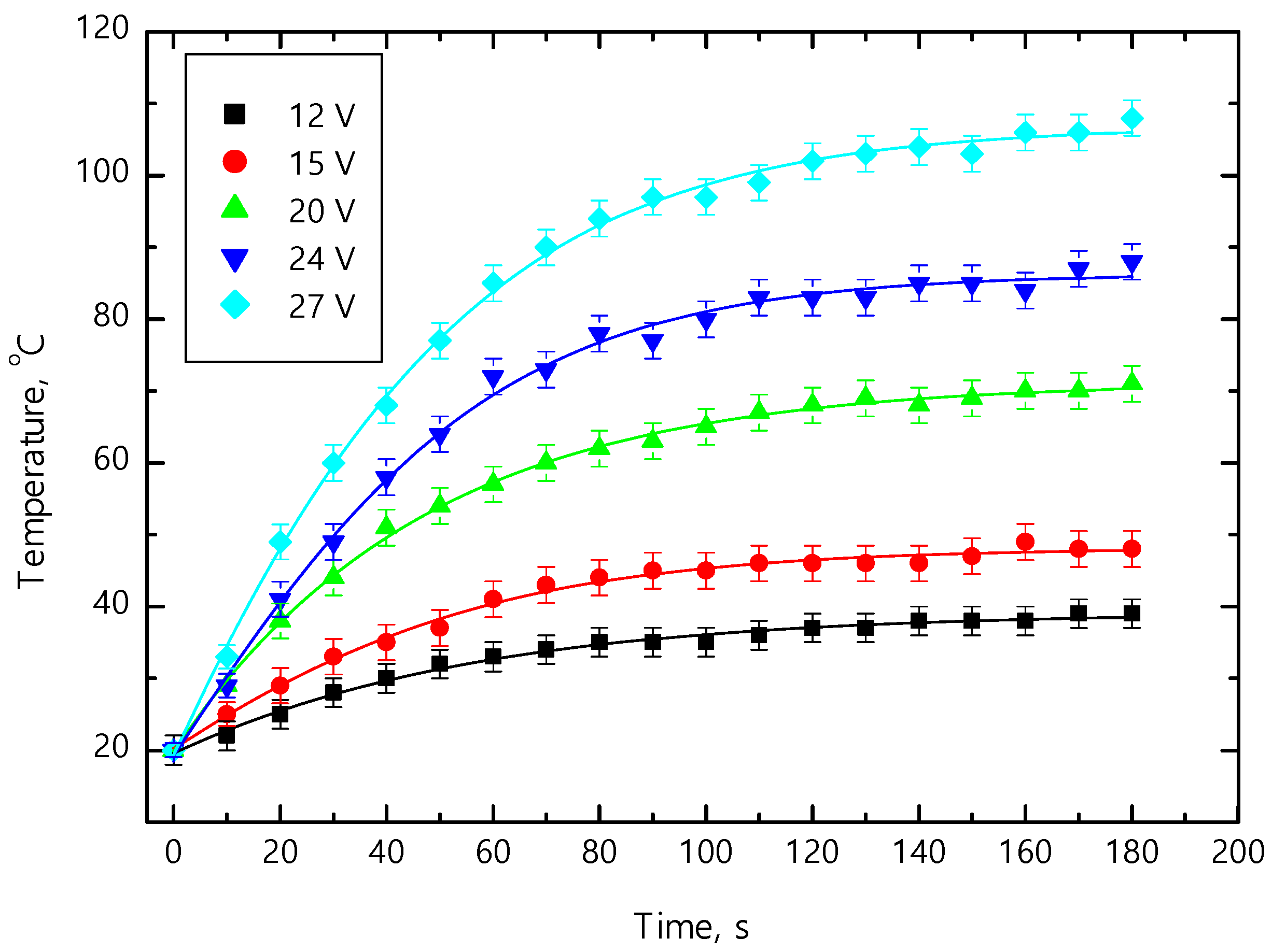
The heating characteristics of the ITO-5 film are given in
Figure 7. Different voltages from 12 to 27 V were used, and the temperature of the glass substrate coated with the ITO-5 film was measured. The applied voltages created various current values, which heat up the specimen. The measurements were performed at the room temperature (20 °C). When 12 V was applied after two minutes, the sample heated up to ~35 °C and saturates. With the increase of applied voltage values from 12 to 27 V, higher temperatures were reached (
Figure 7). When the highest voltage of 27 V was used, the sufficiently high temperature of ~100 °C after 120 s was reached. The further increase of heating time led only to a minor change in the temperature. The heating characteristics indicated that the temperature saturation values of the ITO/glass substrate system were obtained after 120 s.
The steady-state temperatures were obtained for all applied voltages. The rise of saturation temperatures from ~35 to ~105 °C as the voltage increased from 12 to 27 V was observed (
Figure 7). The heat gain by working power (
P) is supplied as Joule heat and is expressed by:
where
Rs is the resistance,
U is the applied voltage, and
I is the current.
The overall Joule heat (
Q) released at a constant applied voltage (which is the energy converted from electrical energy to thermal energy) can be calculated by:
where
I,
Rs and
t are the current, constant electrical resistance and time, respectively. Thus, the increase of voltage directly increases the current values and produces more heat.
We, thus, have a layered structure composed of the ITO film/glass substrate/ambient (20 °C) temperature air layers. The current flowing through the ITO layer raises the temperature of the layer, and the heat is transferred to the glass by conduction, which also heats up. This occurs until a thermal equilibrium is established between the layers and the ambient temperature, and then a constant temperature is obtained [
30].
The experimental results indicated that the current value remained constant throughout heating at a constant applied voltage. The increase of the applied voltages directly increased the current values and produced more heat. The majority of the produced heat was transferred to the glass substrate by conduction; however, part of the heat was lost due to radiation and convection. Thus, with the increase of applied voltage from 12 to 27 V, the temperature rouse from ~35 to ~105 °C.
One of the possible applications of ITO coatings is for defrosting of the icy glass of vehicles (cars, planes, etc.) at negative ambient temperatures. The rapid, non-mechanical removal of frost and ice from windows would be innovative and in-demand in the market. To investigate the thawing properties of the ITO film deposited on glass, the sample was cooled using a Peltier element down to −10 °C.
The results indicated, that when 12 and 15 V were applied, the ice on the surface of specimen was not melted, and the temperatures reached (due to saturation) −5 and −3 °C after 120 s, respectively. The use of a voltage of 20 V allowed the temperature to rise up to 0 °C; however, the glass surface remained frosted. At 24 and 27 V after the 30 s, temperatures of 2 and 5 °C were obtained, respectively. The frost on the glass surface was effectively melted in both cases. A layered system of ITO film/glass substrate/ice layer/environment with a temperature of −10 °C was used for defrosting measurements. The heat is transferred from the ITO layer to the glass and promotes melting of the ice. However, in this case, more of produced thermal energy is used to compensate for a low environment temperature. Therefore, even under a voltage of 20 V, the temperature remained at 0 °C even after 120 s (
Figure 8). The results indicated that the required amount of thermal energy (heat) to completely melt the ice was produced when the applied voltage of 24 V was used. The study showed that the indium-tin-oxide-coated motor vehicle glass could be completely defrosted in a short time at low voltages.


