
Structural and Chemical Peculiarities of Nitrogen-Doped Graphene Grown Using Direct Microwave Plasma-Enhanced Chemical Vapor Deposition


Abstract
:1. Introduction
2. Materials and Methods
2.1. Microwave Plasma-Enhanced CVD of Nitrogen-Doped Graphene
2.2. Characterization
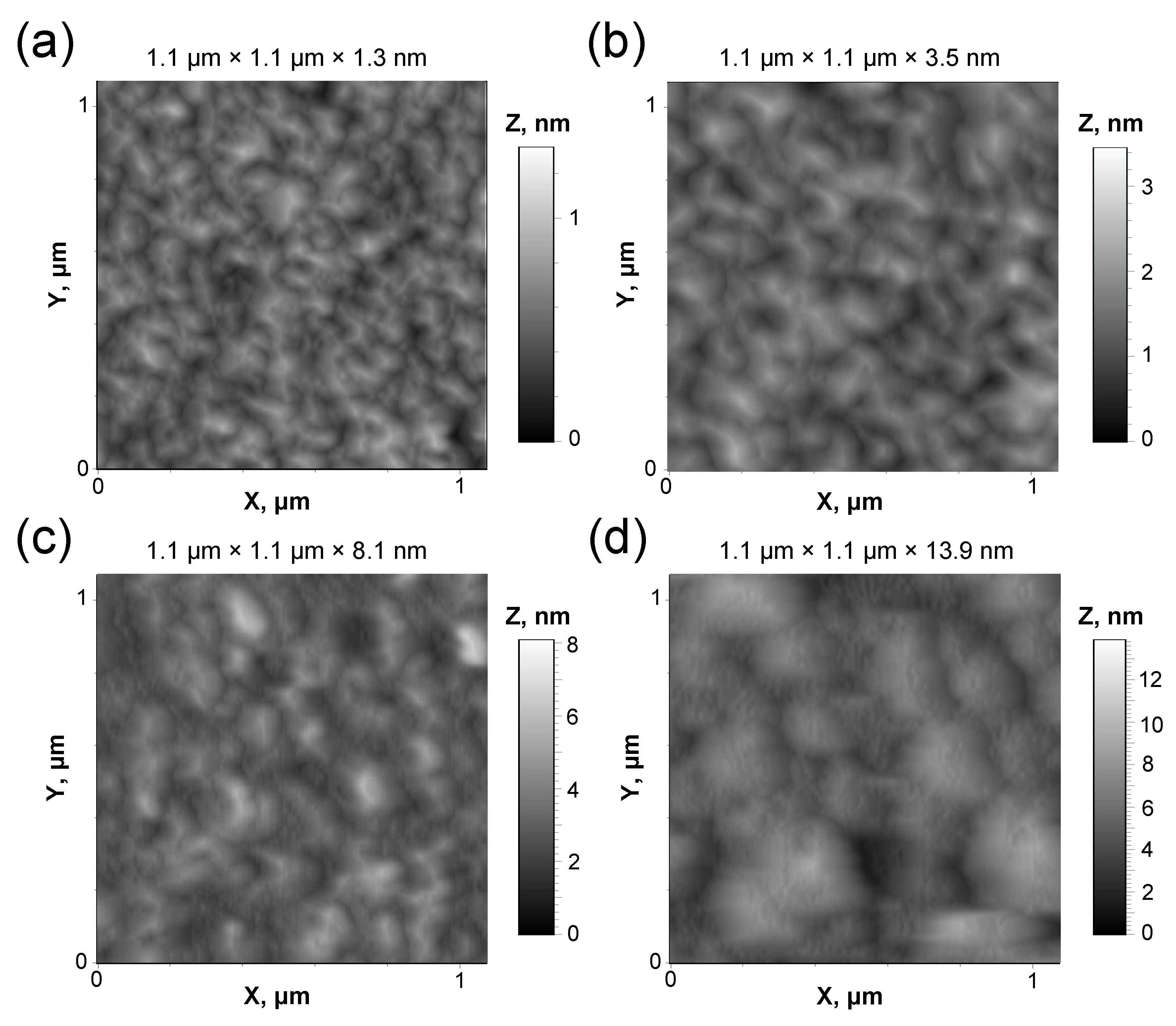
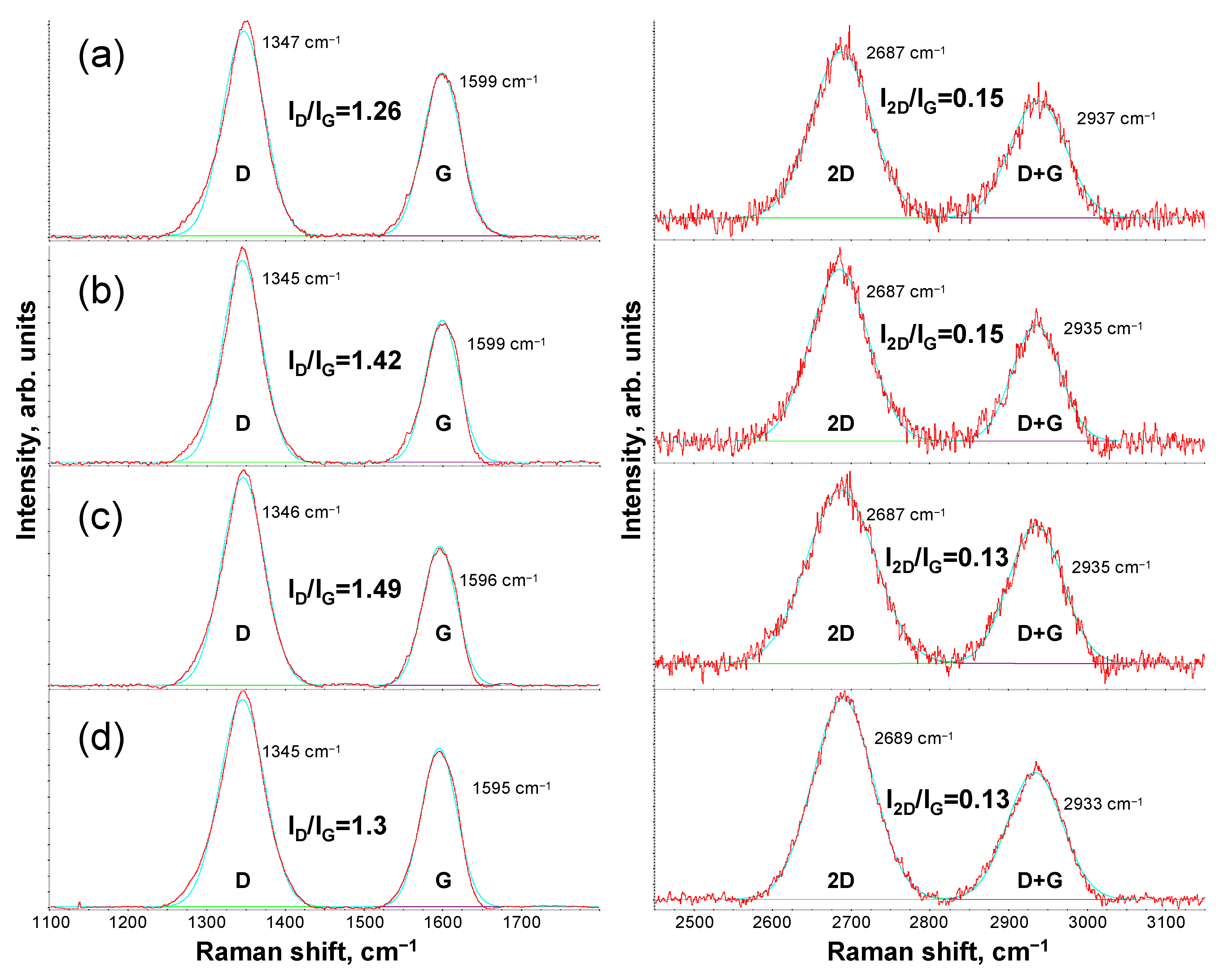
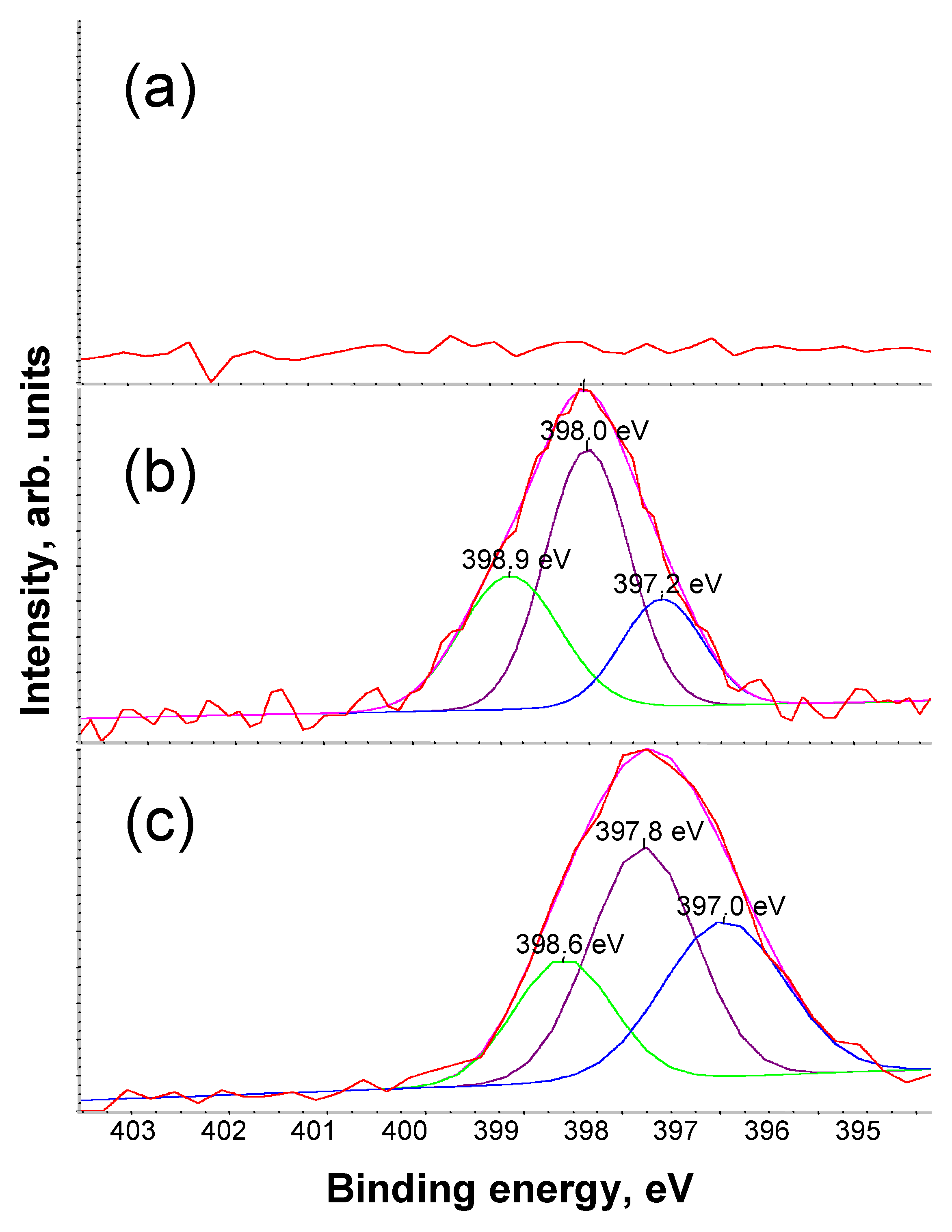
3. Results and Discussion
4. Conclusions
Supplementary Materials
Author Contributions
Funding
Institutional Review Board Statement
Informed Consent Statement
Data Availability Statement
Acknowledgments
Conflicts of Interest
References
- Mas-Balleste, R.; Gomez-Navarro, C.; Gomez-Herrero, J.; Zamora, F. 2D materials: To graphene and beyond. Nanoscale 2011, 3, 20–30. [Google Scholar] [CrossRef] [PubMed]
- Maniadi, A.; Vamvakaki, M.; Suchea, M.; Tudose, I.V.; Popescu, M.; Romanitan, C.; Pachiu, C.; Ionescu, O.N.; Viskadourakis, Z.; Kenanakis, G. Effect of graphene nanoplatelets on the structure, the morphology, and the dielectric behavior of low-density polyethylene nanocomposites. Materials 2020, 13, 4776. [Google Scholar] [CrossRef] [PubMed]
- Wang, Q.H.; Kalantar-Zadeh, K.; Kis, A.; Coleman, J.N.; Strano, M.S. Electronics and optoelectronics of two-dimensional transition metal dichalcogenides. Nat. Nanotechnol. 2012, 7, 699–712. [Google Scholar] [CrossRef] [PubMed]
- Poot, M.; van der Zant, H.S. Nanomechanical properties of few-layer graphene membranes. Appl. Phys. Lett. 2008, 92, 063111. [Google Scholar] [CrossRef]
- Butler, S.Z.; Hollen, S.M.; Cao, L.; Cui, Y.; Gupta, J.A.; Gutiérrez, H.R.; Heinz, T.F.; Hong, S.S.; Huang, J.; Ismach, A.F. Progress, challenges, and opportunities in two-dimensional materials beyond graphene. ACS Nano 2013, 7, 2898–2926. [Google Scholar] [CrossRef]
- Sun, P.; Wang, K.; Zhu, H. Recent developments in graphene-based membranes: Structure, mass-transport mechanism and potential applications. Adv. Mater. 2016, 28, 2287–2310. [Google Scholar] [CrossRef]
- Akinwande, D.; Brennan, C.J.; Bunch, J.S.; Egberts, P.; Felts, J.R.; Gao, H.; Huang, R.; Kim, J.-S.; Li, T.; Li, Y. A review on mechanics and mechanical properties of 2D materials—Graphene and beyond. Extrem. Mech. Lett. 2017, 13, 42–77. [Google Scholar] [CrossRef] [Green Version]
- Maiti, U.N.; Lee, W.J.; Lee, J.M.; Oh, Y.; Kim, J.Y.; Kim, J.E.; Shim, J.; Han, T.H.; Kim, S.O. 25th anniversary article: Chemically modified/doped carbon nanotubes & graphene for optimized nanostructures & nanodevices. Adv. Mater. 2014, 26, 40–67. [Google Scholar]
- Lv, R.; Terrones, M. Towards new graphene materials: Doped graphene sheets and nanoribbons. Mater. Lett. 2012, 78, 209–218. [Google Scholar] [CrossRef]
- Georgakilas, V.; Otyepka, M.; Bourlinos, A.B.; Chandra, V.; Kim, N.; Kemp, K.C.; Hobza, P.; Zboril, R.; Kim, K.S. Functionalization of graphene: Covalent and non-covalent approaches, derivatives and applications. Chem. Rev. 2012, 112, 6156–6214. [Google Scholar] [CrossRef]
- Dong, X.; Long, Q.; Wei, A.; Zhang, W.; Li, L.-J.; Chen, P.; Huang, W. The electrical properties of graphene modified by bromophenyl groups derived from a diazonium compound. Carbon 2012, 50, 1517–1522. [Google Scholar] [CrossRef]
- Tripathi, N.; Pavelyev, V.; Sharma, P.; Kumar, S.; Rymzhina, A.; Mishra, P. Review of titanium trisulfide (TiS3): A novel material for next generation electronic and optical devices. Mater. Sci. Semicond. Process. 2021, 127, 105699. [Google Scholar] [CrossRef]
- Wei, D.; Liu, Y.; Wang, Y.; Zhang, H.; Huang, L.; Yu, G. Synthesis of N-doped graphene by chemical vapor deposition and its electrical properties. Nano Lett. 2009, 9, 1752–1758. [Google Scholar] [CrossRef]
- Peres, N.; Guinea, F.; Neto, A.C. Coulomb interactions and ferromagnetism in pure and doped graphene. Phys. Rev. B 2005, 72, 174406. [Google Scholar] [CrossRef] [Green Version]
- Uchoa, B.; Neto, A.C. Superconducting states of pure and doped graphene. Phys. Rev. Lett. 2007, 98, 146801. [Google Scholar] [CrossRef] [PubMed] [Green Version]
- Wang, X.; Sun, G.; Routh, P.; Kim, D.-H.; Huang, W.; Chen, P. Heteroatom-doped graphene materials: Syntheses, properties and applications. Chem. Soc. Rev. 2014, 43, 7067–7098. [Google Scholar] [CrossRef] [PubMed] [Green Version]
- Wu, P.; Cai, Z.; Gao, Y.; Zhang, H.; Cai, C. Enhancing the electrochemical reduction of hydrogen peroxide based on nitrogen-doped graphene for measurement of its releasing process from living cells. Chem. Commun. 2011, 47, 11327–11329. [Google Scholar] [CrossRef]
- Li, N.; Wang, Z.; Zhao, K.; Shi, Z.; Gu, Z.; Xu, S. Large scale synthesis of N-doped multi-layered graphene sheets by simple arc-discharge method. Carbon 2010, 48, 255–259. [Google Scholar] [CrossRef]
- Jeong, H.M.; Lee, J.W.; Shin, W.H.; Choi, Y.J.; Shin, H.J.; Kang, J.K.; Choi, J.W. Nitrogen-doped graphene for high-performance ultracapacitors and the importance of nitrogen-doped sites at basal planes. Nano Lett. 2011, 11, 2472–2477. [Google Scholar] [CrossRef]
- Ion-Ebrașu, D.; Andrei, R.D.; Enache, S.; Căprărescu, S.; Negrilă, C.C.; Jianu, C.; Enache, A.; Boerașu, I.; Carcadea, E.; Varlam, M. Nitrogen functionalization of cvd grown three-dimensional graphene foam for hydrogen evolution reactions in alkaline media. Materials 2021, 14, 4952. [Google Scholar] [CrossRef]
- Kamedulski, P.; Truszkowski, S.; Lukaszewicz, J.P. Highly effective methods of obtaining N-doped graphene by gamma irradiation. Materials 2020, 13, 4975. [Google Scholar] [CrossRef] [PubMed]
- Komissarov, I.V.; Kovalchuk, N.G.; Labunov, V.A.; Girel, K.V.; Korolik, O.V.; Tivanov, M.S.; Lazauskas, A.; Andrulevičius, M.; Tamulevičius, T.; Grigaliūnas, V. Nitrogen-doped twisted graphene grown on copper by atmospheric pressure CVD from a decane precursor. Beilstein J. Nanotechnol. 2017, 8, 145–158. [Google Scholar] [CrossRef] [PubMed] [Green Version]
- Lü, X.; Wu, J.; Lin, T.; Wan, D.; Huang, F.; Xie, X.; Jiang, M. Low-temperature rapid synthesis of high-quality pristine or boron-doped graphene via Wurtz-type reductive coupling reaction. J. Mater. Chem. 2011, 21, 10685–10689. [Google Scholar] [CrossRef]
- Jeon, I.-Y.; Choi, H.-J.; Ju, M.J.; Choi, I.T.; Lim, K.; Ko, J.; Kim, H.K.; Kim, J.C.; Lee, J.-J.; Shin, D. Direct nitrogen fixation at the edges of graphene nanoplatelets as efficient electrocatalysts for energy conversion. Sci. Rep. 2013, 3, 2260. [Google Scholar] [CrossRef] [Green Version]
- Rani, P.; Jindal, V. Designing band gap of graphene by B and N dopant atoms. RSC Adv. 2013, 3, 802–812. [Google Scholar] [CrossRef] [Green Version]
- Lherbier, A.; Botello-Méndez, A.R.; Charlier, J.-C. Electronic and transport properties of unbalanced sublattice N-doping in graphene. Nano Lett. 2013, 13, 1446–1450. [Google Scholar] [CrossRef]
- Liu, Z.W.; Peng, F.; Wang, H.J.; Yu, H.; Zheng, W.X.; Yang, J. Phosphorus-doped graphite layers with high electrocatalytic activity for the O2 reduction in an alkaline medium. Angew. Chem. Int. Ed. 2011, 50, 3257–3261. [Google Scholar] [CrossRef]
- Denis, P.A. Band gap opening of monolayer and bilayer graphene doped with aluminium, silicon, phosphorus, and sulfur. Chem. Phys. Lett. 2010, 492, 251–257. [Google Scholar] [CrossRef]
- Ribas, M.A.; Singh, A.K.; Sorokin, P.B.; Yakobson, B.I. Patterning nanoroads and quantum dots on fluorinated graphene. Nano Res. 2011, 4, 143–152. [Google Scholar] [CrossRef] [Green Version]
- Yang, M.; Zhou, L.; Wang, J.; Liu, Z.; Liu, Z. Evolutionary chlorination of graphene: From charge-transfer complex to covalent bonding and nonbonding. J. Phys. Chem. C 2012, 116, 844–850. [Google Scholar] [CrossRef]
- Venkatesan, N.; Archana, K.S.; Suresh, S.; Aswathy, R.; Ulaganthan, M.; Periasamy, P.; Ragupathy, P. Boron-Doped Graphene as Efficient Electrocatalyst for Zinc-Bromine Redox Flow Batteries. ChemElectroChem 2019, 6, 1107–1114. [Google Scholar] [CrossRef]
- Kalita, G.; Wakita, K.; Takahashi, M.; Umeno, M. Iodine doping in solid precursor-based CVD growth graphene film. J. Mater. Chem. 2011, 21, 15209–15213. [Google Scholar] [CrossRef]
- Yu, X.; Li, N.; Zhang, S.; Liu, C.; Chen, L.; Xi, M.; Song, Y.; Ali, S.; Iqbal, O.; Han, M. Enhancing the energy storage capacity of graphene supercapacitors via solar heating. J. Mater. Chem. A 2022, 10, 3382–3392. [Google Scholar] [CrossRef]
- Chen, J.; Bailey, J.J.; Britnell, L.; Perez-Page, M.; Sahoo, M.; Zhang, Z.; Strudwick, A.; Hack, J.; Guo, Z.; Ji, Z. The performance and durability of high-temperature proton exchange membrane fuel cells enhanced by single-layer graphene. Nano Energy 2022, 93, 106829. [Google Scholar] [CrossRef]
- Mu, Y.; Han, M.; Li, J.; Liang, J.; Yu, J. Growing vertical graphene sheets on natural graphite for fast charging lithium-ion batteries. Carbon 2021, 173, 477–484. [Google Scholar] [CrossRef]
- Safie, N.E.; Azam, M.A.; Aziz, M.F.; Ismail, M. Recent progress of graphene-based materials for efficient charge transfer and device performance stability in perovskite solar cells. Int. J. Energy Res. 2021, 45, 1347–1374. [Google Scholar] [CrossRef]
- Xie, T.; Wang, Q.; Wallace, R.M.; Gong, C. Understanding and optimization of graphene gas sensors. Appl. Phys. Lett. 2021, 119, 013104. [Google Scholar] [CrossRef]
- Shinde, S.M.; Kano, E.; Kalita, G.; Takeguchi, M.; Hashimoto, A.; Tanemura, M. Grain structures of nitrogen-doped graphene synthesized by solid source-based chemical vapor deposition. Carbon 2016, 96, 448–453. [Google Scholar] [CrossRef]
- Mattevi, C.; Kim, H.; Chhowalla, M. A review of chemical vapour deposition of graphene on copper. J. Mater. Chem. 2011, 21, 3324–3334. [Google Scholar] [CrossRef]
- Huang, L.; Chang, Q.; Guo, G.; Liu, Y.; Xie, Y.; Wang, T.; Ling, B.; Yang, H. Synthesis of high-quality graphene films on nickel foils by rapid thermal chemical vapor deposition. Carbon 2012, 50, 551–556. [Google Scholar] [CrossRef]
- Kang, J.; Shin, D.; Bae, S.; Hong, B.H. Graphene transfer: Key for applications. Nanoscale 2012, 4, 5527–5537. [Google Scholar] [CrossRef] [PubMed]
- Hong, S.K.; Song, S.M.; Sul, O.; Cho, B.J. Carboxylic group as the origin of electrical performance degradation during the transfer process of CVD growth graphene. J. Electrochem. Soc. 2012, 159, K107. [Google Scholar] [CrossRef]
- Ambrosi, A.; Pumera, M. The CVD graphene transfer procedure introduces metallic impurities which alter the graphene electrochemical properties. Nanoscale 2014, 6, 472–476. [Google Scholar] [CrossRef] [PubMed] [Green Version]
- Boas, C.; Focassio, B.; Marinho, E.; Larrude, D.; Salvadori, M.; Leão, C.R.; Dos Santos, D.J. Characterization of nitrogen doped graphene bilayers synthesized by fast, low temperature microwave plasma-enhanced chemical vapour deposition. Sci. Rep. 2019, 9, 13715. [Google Scholar] [CrossRef]
- Kim, J.H.; Castro, E.J.D.; Hwang, Y.G.; Lee, C.H. Synthesis of Few-Layer Graphene Using DC PE-CVD. AIP Conf. Proc. 2011, 1399, 801–802. [Google Scholar]
- Childres, I.; Jauregui, L.A.; Park, W.; Cao, H.; Chen, Y.P. Raman spectroscopy of graphene and related materials. New Dev. Photon Mater. Res. 2013, 1, 1–20. [Google Scholar]
- Zafar, Z.; Ni, Z.H.; Wu, X.; Shi, Z.X.; Nan, H.Y.; Bai, J.; Sun, L.T. Evolution of Raman spectra in nitrogen doped graphene. Carbon 2013, 61, 57–62. [Google Scholar] [CrossRef]
- Zheng, S.; Zhong, G.; Wu, X.; D’Arsiè, L.; Robertson, J. Metal-catalyst-free growth of graphene on insulating substrates by ammonia-assisted microwave plasma-enhanced chemical vapor deposition. RSC Adv. 2017, 7, 33185–33193. [Google Scholar] [CrossRef] [Green Version]
- Wang, C.; Yuen, M.F.; Ng, T.W.; Jha, S.K.; Lu, Z.; Kwok, S.Y.; Wong, T.L.; Yang, X.; Lee, C.S.; Lee, S.T. Plasma-assisted growth and nitrogen doping of graphene films. Appl. Phys. Lett. 2012, 100, 253107. [Google Scholar] [CrossRef]
- Merel, P.; Tabbal, M.; Chaker, M.; Moisa, S.; Margot, J. Direct evaluation of the sp3 content in diamond-like-carbon films by XPS. Appl. Surf. Sci. 1998, 136, 105–110. [Google Scholar] [CrossRef]
- Marinoiu, A.; Raceanu, M.; Andrulevicius, M.; Tamuleviciene, A.; Tamulevicius, T.; Nica, S.; Bala, D.; Varlam, M. Low-cost preparation method of well dispersed gold nanoparticles on reduced graphene oxide and electrocatalytic stability in PEM fuel cell. Arab. J. Chem. 2020, 13, 3585–3600. [Google Scholar] [CrossRef]
- JankauskaitĿ, V.; VitkauskienĿ, A.; Lazauskas, A.; Baltrusaitis, J.; ProsyĿevas, I.; AndruleviĿius, M. Bactericidal effect of graphene oxide/Cu/Ag nanoderivatives against Escherichia coli, Pseudomonas aeruginosa, Klebsiella pneumoniae, Staphylococcus aureus and Methicillin-resistant Staphylococcus aureus. Int. J. Pharm. 2016, 511, 90–97. [Google Scholar] [CrossRef] [PubMed]
- He, H.; Yang, Q.; Xiao, S.; Han, X.; Li, Q.; Lv, K.; Hong, J.; Tang, D.; Kejian, D. Investigation of Edge-selectively Nitrogen-doped Metal Free Graphene For Oxygen Reduction Reaction. J. Adv. Nanotechnol. 2020, 1, 5–13. [Google Scholar]
- Tian, K.; Wang, J.; Cao, L.; Yang, W.; Guo, W.; Liu, S.; Li, W.; Wang, F.; Li, X.; Xu, Z. Single-site pyrrolic-nitrogen-doped sp2-hybridized carbon materials and their pseudocapacitance. Nat. Commun. 2020, 11, 3884. [Google Scholar] [CrossRef]
- Liu, F.; Zhang, Z.; Rong, X.; Yu, Y.; Wang, T.; Sheng, B.; Wei, J.; Zhou, S.; Yang, X.; Xu, F. Graphene-Assisted Epitaxy of Nitrogen Lattice Polarity GaN Films on Non-Polar Sapphire Substrates for Green Light Emitting Diodes. Adv. Funct. Mater. 2020, 30, 2001283. [Google Scholar] [CrossRef]
- Wu, Z.; Wang, Y.; Li, S.; Wang, X.; Xu, Z.; Zhou, F. Mechanical and tribological properties of BCN coatings sliding against different wood balls. Sci. Eng. Compos. Mater. 2019, 26, 402–411. [Google Scholar] [CrossRef]
- Zhou, J.; Ye, F.; Cui, X.; Cheng, L.; Li, J.; Liu, Y.; Zhang, L. Mechanical and dielectric properties of two types of Si3N4 fibers annealed at elevated temperatures. Materials 2018, 11, 1498. [Google Scholar] [CrossRef] [Green Version]
- Tao, F.; Wang, Z.H.; Qiao, M.H.; Liu, Q.; Sim, W.S.; Xu, G.Q. Covalent attachment of acetonitrile on Si (100) through Si–C and Si–N linkages. J. Chem. Phys. 2001, 115, 8563–8569. [Google Scholar] [CrossRef] [Green Version]
- Luo, Z.; Lim, S.; Tian, Z.; Shang, J.; Lai, L.; MacDonald, B.; Fu, C.; Shen, Z.; Yu, T.; Lin, J. Pyridinic N doped graphene: Synthesis, electronic structure, and electrocatalytic property. J. Mater. Chem. 2011, 21, 8038–8044. [Google Scholar] [CrossRef]
- Legesse, M.; El Mellouhi, F.; Bentria, E.T.; Madjet, M.E.; Fisher, T.S.; Kais, S.; Alharbi, F.H. Reduced work function of graphene by metal adatoms. Appl. Surf. Sci. 2017, 394, 98–107. [Google Scholar] [CrossRef] [Green Version]
- Sheng, Z.-H.; Shao, L.; Chen, J.-J.; Bao, W.-J.; Wang, F.-B.; Xia, X.-H. Catalyst-free synthesis of nitrogen-doped graphene via thermal annealing graphite oxide with melamine and its excellent electrocatalysis. ACS Nano 2011, 5, 4350–4358. [Google Scholar] [CrossRef] [PubMed]
- Wei, D.; Peng, L.; Li, M.; Mao, H.; Niu, T.; Han, C.; Chen, W.; Wee, A.T.S. Low temperature critical growth of high quality nitrogen doped graphene on dielectrics by plasma-enhanced chemical vapor deposition. ACS Nano 2015, 9, 164–171. [Google Scholar] [CrossRef] [PubMed]


| Sample No. | Morphological Parameter | |||
|---|---|---|---|---|
| Zmean, nm | Rq, nm | Rsk | Rku | |
| N0 | 0.76 ± 0.2 | 0.16 ± 0.2 | 0.19 ± 0.2 | 3.32 ± 0.2 |
| N35 | 1.65 ± 0.2 | 0.49 ± 0.2 | 0.35 ± 0.2 | 3.09 ± 0.2 |
| N75 | 3.12 ± 0.2 | 1.33 ± 0.2 | 0.93 ± 0.2 | 4.12 ± 0.2 |
| N110 | 7.30 ± 0.2 | 2.32 ± 0.2 | 0.18 ± 0.2 | 3.14 ± 0.2 |
| Peak | Atomic Concentration (%) | ||
|---|---|---|---|
| N0 | N35 | N100 | |
| O 1s | 18.48 | 21.25 | 21.63 |
| N 1s | 0 | 1.04 | 2.08 |
| C 1s | 47.69 | 36.37 | 36.29 |
| Si 2p | 33.83 | 41.35 | 40 |
Publisher’s Note: MDPI stays neutral with regard to jurisdictional claims in published maps and institutional affiliations. |
© 2022 by the authors. Licensee MDPI, Basel, Switzerland. This article is an open access article distributed under the terms and conditions of the Creative Commons Attribution (CC BY) license (https://creativecommons.org/licenses/by/4.0/).
Share and Cite
Meškinis, Š.; Gudaitis, R.; Andrulevičius, M.; Lazauskas, A. Structural and Chemical Peculiarities of Nitrogen-Doped Graphene Grown Using Direct Microwave Plasma-Enhanced Chemical Vapor Deposition. Coatings 2022, 12, 572. https://doi.org/10.3390/coatings12050572
Meškinis Š, Gudaitis R, Andrulevičius M, Lazauskas A. Structural and Chemical Peculiarities of Nitrogen-Doped Graphene Grown Using Direct Microwave Plasma-Enhanced Chemical Vapor Deposition. Coatings. 2022; 12(5):572. https://doi.org/10.3390/coatings12050572
Chicago/Turabian StyleMeškinis, Šarūnas, Rimantas Gudaitis, Mindaugas Andrulevičius, and Algirdas Lazauskas. 2022. "Structural and Chemical Peculiarities of Nitrogen-Doped Graphene Grown Using Direct Microwave Plasma-Enhanced Chemical Vapor Deposition" Coatings 12, no. 5: 572. https://doi.org/10.3390/coatings12050572
APA StyleMeškinis, Š., Gudaitis, R., Andrulevičius, M., & Lazauskas, A. (2022). Structural and Chemical Peculiarities of Nitrogen-Doped Graphene Grown Using Direct Microwave Plasma-Enhanced Chemical Vapor Deposition. Coatings, 12(5), 572. https://doi.org/10.3390/coatings12050572