
Influence of Plasma Surface Treatment of Polyimide on the Microstructure of Aluminum Thin Films

Abstract
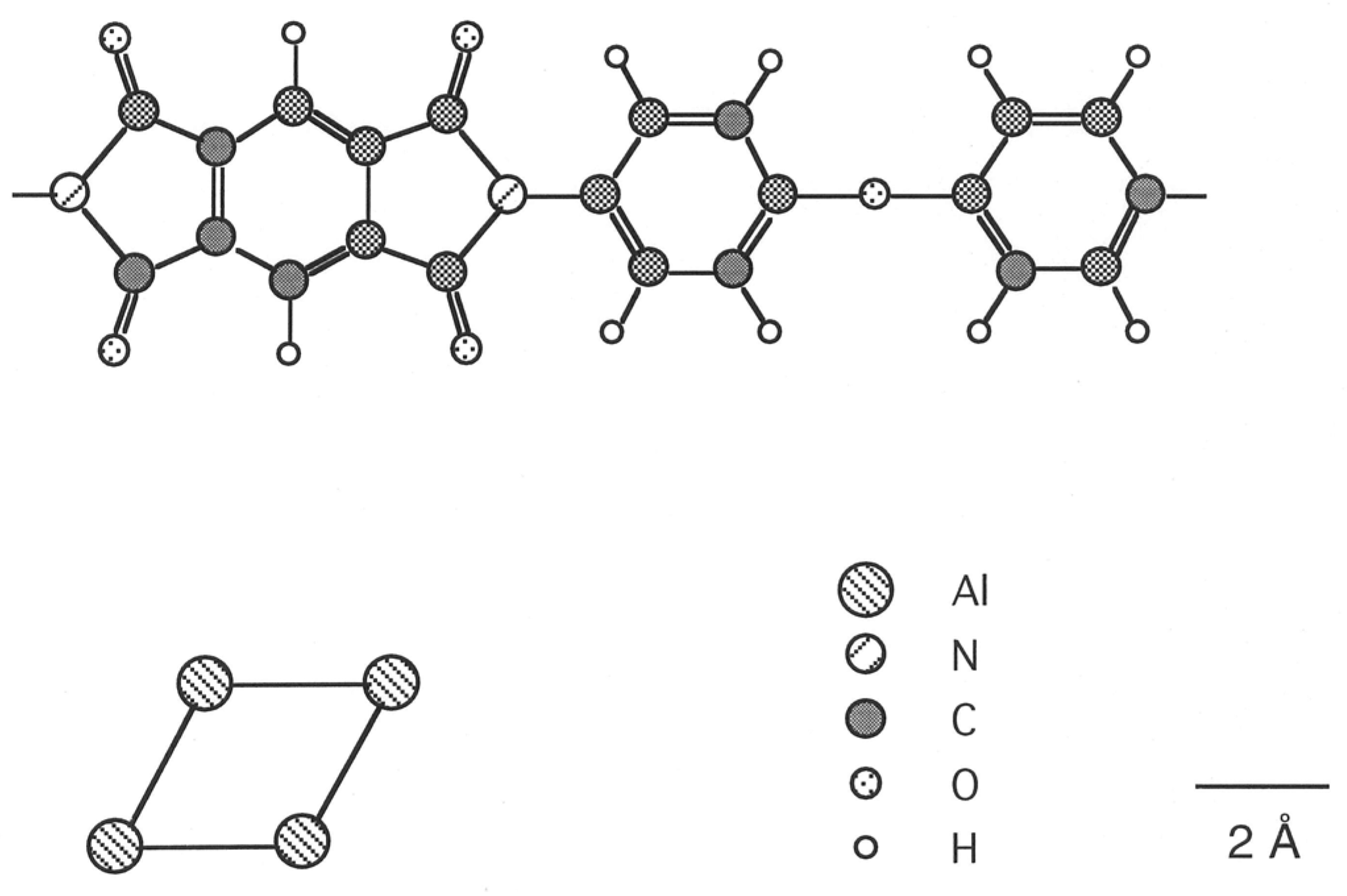
1. Introduction
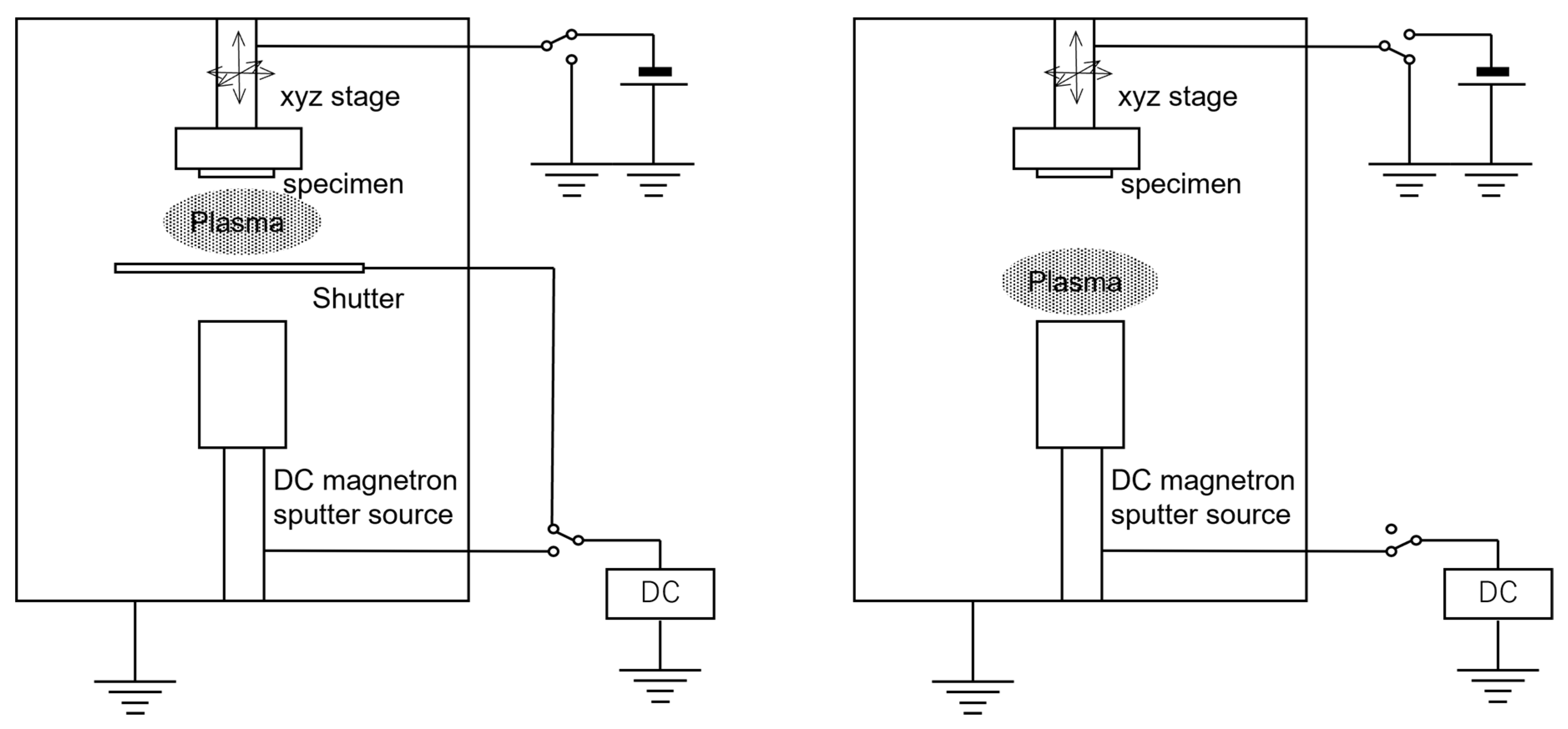
2. Experimental
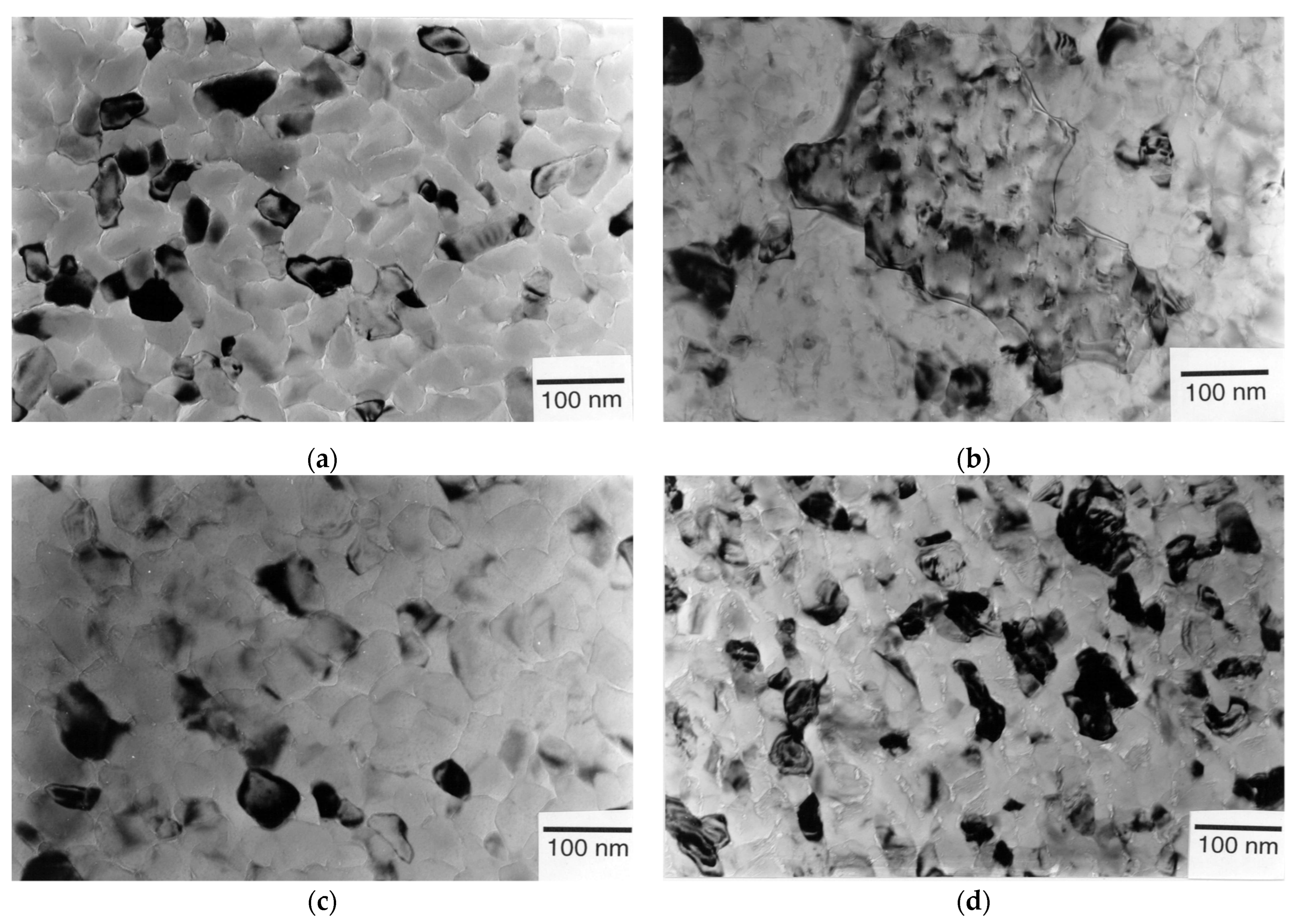
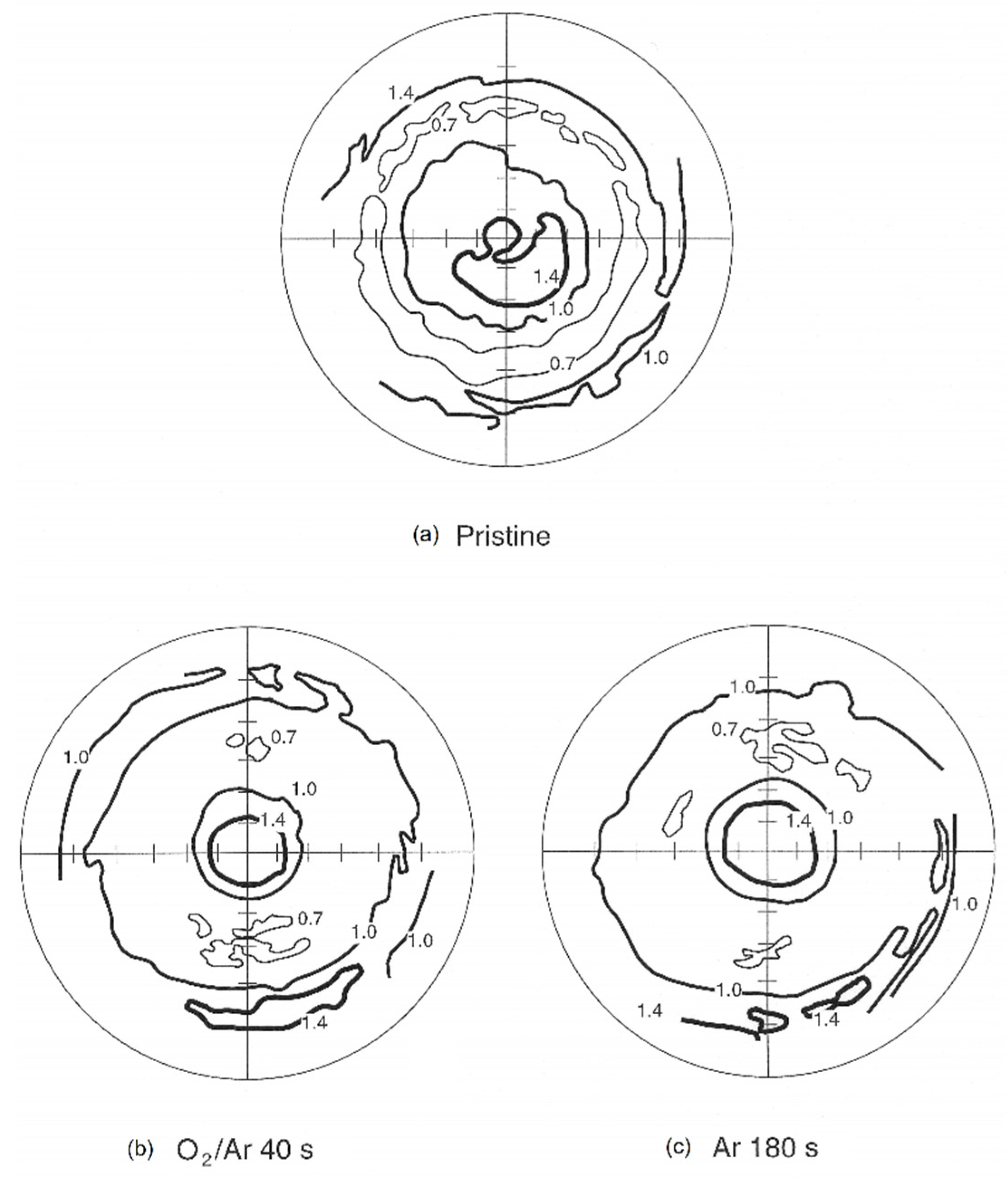
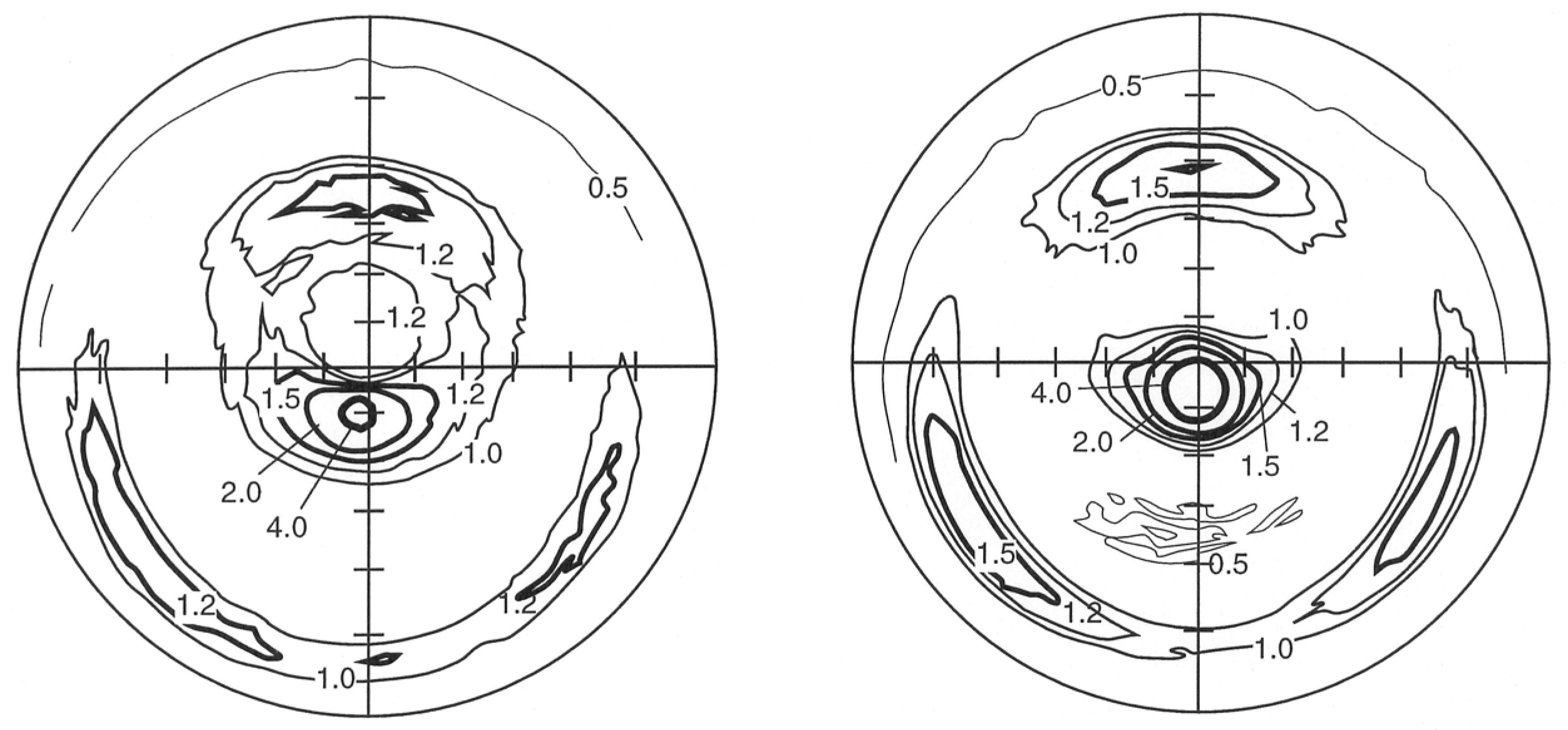
3. Results and Discussion
4. Conclusions
Funding
Institutional Review Board Statement
Informed Consent Statement
Data Availability Statement
Conflicts of Interest
References
- Attardo, M.J.; Rutledge, R.; Jack, R.C. Statistical Metallurgical Model for Electromigration Failure in Aluminum Thin-Film Conductors. J. Appl. Phys. 1971, 42, 4343–4349. [Google Scholar] [CrossRef]
- Schoen, J.M. Monte Carlo calculations of structure-induced electromigration failure. J. Appl. Phys. 1980, 51, 513–521. [Google Scholar] [CrossRef]
- Cho, J.; Thompson, C.V. Grain size dependence of electromigration-induced failures in narrow interconnects. Appl. Phys. Lett. 1989, 54, 2577–2579. [Google Scholar] [CrossRef]
- Vaidya, S.; Sheng, T.T.; Sinha, A.K. Linewidth dependence of electromigration in evaporated Al-0.5%Cu. Appl. Phys. Lett. 1980, 36, 464–466. [Google Scholar] [CrossRef]
- Vaidya, S.; Sinha, A.K. Effect of texture and grain structure on electromigration in Al-0.5%Cu thin films. Thin Solid Film. 1981, 75, 253–259. [Google Scholar] [CrossRef]
- Knorr, D.B.; Rodbell, K.P. The role of texture in the electromigration behavior of pure aluminum lines. J. Appl. Phys. 1996, 79, 2409–2417. [Google Scholar] [CrossRef]
- Liu, X.; Li, Y.; Liu, Y.; Sun, D.; Guo, W.; Sun, X.; Feng, Y.; Chi, H.; Li, X.; Tian, F.; et al. Performance and microstructure characteristics in polyimide/nano-aluminum composites. Surf. Coat. Technol. 2017, 320, 103–108. [Google Scholar] [CrossRef]
- Lucchini, R.; Cattarinuzzi, E.; Maraghechi, S.; Gastaldi, D.; Adami, A.; Lorenzelli, L.; Vena, P. Delamination phenomena in aluminum/polyimide deformable interconnects: In-situ micro-tensile testing. Mater. Des. 2016, 89, 121–128. [Google Scholar] [CrossRef]
- Liu, D.S.; Tsai, C.Y.; Lu, Y.T.; Sung, C.K.; Chung, C.L. Finite element method investigation into nanoimprinting of aluminum/polyimide bi-layer substrates. Mircoelectr. Eng. 2010, 87, 2361–2367. [Google Scholar] [CrossRef]
- d’Heurle, F.; Berenbaum, L.; Rosenberg, R. On the structure of aluminum films. Trans. Metall. Soc. AIME 1968, 242, 502–511. [Google Scholar]
- Jawarani, D.; Stark, J.P.; Kawasaki, H.; Olowolafe, J.O.; Lee, C.C.; Klein, J.; Pintchovski, F. Intermetallic Compound Formation in Ti/Al Alloy Thin Film Couples and Its Role in Electromigration Lifetime. J. Electrochem. Soc. 1994, 141, 302–305. [Google Scholar] [CrossRef]
- Knorr, D.B.; Szpunar, J.A. Applications of texture in thin films. J. Met. 1994, 46, 42–48. [Google Scholar] [CrossRef]
- Sinha, A.K.; Sheng, T.T. The temperature dependence of stresses in aluminum films on oxidized silicon substrates. Thin Solid Film. 1978, 48, 117–126. [Google Scholar] [CrossRef]
- Roberts, S.; Dobson, P.J. The microstructure of aluminium thin films on amorphous SiO2. Thin Solid Film. 1986, 135, 137–148. [Google Scholar] [CrossRef]
- Knorr, D.B.; Tracy, D.P.; Lu, T.-M. Texture development in thin metallic films. Textures Microstruct. 1991, 14, 543–554. [Google Scholar] [CrossRef]
- Grovenor, C.R.M.; Hentzell, H.T.G.; Smith, D.A. The development of grain structure during growth of metallic films. Acta Metall. 1984, 32, 773–781. [Google Scholar] [CrossRef]
- Silvain, J.F.; Veyrat, A.; Ehrhardt, J.J. Influence of oxygen partial pressure on the adhesion of metallic films evaporated on PET. Thin Solid Film. 1994, 237, 164–171. [Google Scholar] [CrossRef]
- Verkerk, M.J.; Van der Kolk, G.J. Effects of oxygen on the growth of vapor-deposited aluminum films. J. Vac. Sci. Technol. A 1986, 4, 3101–3105. [Google Scholar] [CrossRef]
- Ferl, J.E.; Edward, J.; Long, R. Infrared spectroscopic analysis of the effects of simulated space radiation on a polyimide. IEEE Trans. Nucl. Sci. 1981, 28, 4119–4124. [Google Scholar] [CrossRef]
- Matienzo, L.J.; Emmi, F.; Hart, D.C.V.; Gall, T.P. Interactions of high-energy ion beams with polyimide films. J. Vac. Sci. Technol. A 1989, 7, 1784–1789. [Google Scholar] [CrossRef]
- Egitto, F.D.; Matienzo, L.J.; Blackwell, K.J.; Knoll, A.R. Oxygen plasma modification of polyimide webs: Effect of ion bombardment on metal adhesion. J. Adhes. Sci. Technol. 1994, 8, 411–433. [Google Scholar] [CrossRef]
- Inagaki, N.; Tasaka, S.; Hibi, K. Improved adhesion between plasma-treated polyimide film and evaporated copper. J. Adhes. Sci. Technol. 1994, 8, 395–410. [Google Scholar] [CrossRef]
- Fatyeyeva, K.; Dahi, A.; Chappey, C.; Langevin, D.; Valleton, J.-M.; Poncin-Epaillard, F.; Marais, S. Effect of cold plasma treatment on surface properties and gas permeability of polyimide films. RSC Adv. 2014, 4, 31036–31046. [Google Scholar] [CrossRef]
- Tanigawa, S.; Nakamae, K.; Matsumoto, T. Effect of the radio frequency O2 plasma treatment at polyimide surface on the adhesion of the vacuum deposited thin Fe Film. Kobunshi Ronbunshu 1990, 47, 41–48. [Google Scholar] [CrossRef][Green Version]
- Altanasoska, L.; Anderson, S.G.; Meyer, H.M., III; Lin, Y.; Weaver, J.H. Aluminum/polyimide interface formation: An x-ray photoelectron spectroscopy study of selective chemical bonding. J. Vac. Sci. Technol. A 1987, 5, 3325–3333. [Google Scholar] [CrossRef]
- Bartha, J.W.; Hahn, P.O.; LeGoues, F.; Ho, P.S. Photoemission spectroscopy study of aluminum–polyimide interface. J. Vac. Sci. Technol. A 1995, 3, 1390–1393. [Google Scholar] [CrossRef]
- Pireaux, J.J. Is there an interaction at the aromatic site(s) in a metal/polymer interface? An XPS and HREELS review. Synth. Met. 1994, 67, 39–46. [Google Scholar] [CrossRef]
- Park, S.J.; Lee, E.J.; Kwon, S.H. Influence of atmospheric-pressure plasma treatment on surface of polyimide film. Solid State Phenom. 2007, 119, 123–126. [Google Scholar] [CrossRef]
- Usami, K.; Ishijima, T.; Toyoda, H. Rapid plasma treatment of polyimide for improved adhesive and durable copper film deposition. Thin Solid Film. 2012, 521, 22–26. [Google Scholar] [CrossRef]
- Ho, P.S.; Hahn, P.O.; Bartha, J.W.; Rubloff, G.W.; LeGoues, P.K.; Silverman, B.D. Chemical bonding and reaction at metal/polymer interfaces. J. Vac. Sci. Technol. A 1985, 3, 739–745. [Google Scholar] [CrossRef]
- Cen-Puc, M.; Schander, A.; Vargas Gleason, M.G.; Lang, W. An Assessment of Surface Treatments for Adhesion of Polyimide Thin Films. Polymers 2021, 13, 1955. [Google Scholar] [CrossRef] [PubMed]
- Kenty, J.L.; Hirth, J.P. Epitaxy and heterogeneous nucleation theory. Surf. Sci. 1969, 15, 403–424. [Google Scholar] [CrossRef]
- Baglin, J. Ion beam modification of insulators. Surf. Sci. Lett. 1987, 191, A524. [Google Scholar]
- Bachman, B.J.; Vasile, M.L. Ion bombardment of polyimide films. J. Vac. Sci. Technol. A 1980, 7, 2709–2716. [Google Scholar] [CrossRef]
- Oberlin, A.; Ayache, J.; Oberlin, M. High-resolution dark-field imaging in epoxy and polyimide systems. J. Polym. Sci. Polym. Phys. Ed. 1982, 20, 579–591. [Google Scholar] [CrossRef]
- Russel, T.R. A small-angle X-ray scattering study of an aromatic polyimide. J. Polym. Sci. Polym. Phys. Ed. 1984, 22, 1105–1117. [Google Scholar] [CrossRef]
- Iona, F. Preparation and properties of clean surfaces of aluminum. J. Phys. Chem. Solids 1967, 28, 2155–2158. [Google Scholar]
- Mullins, W.W. The effect of thermal grooving on grain boundary motion. Acta Metall. 1958, 6, 414–427. [Google Scholar] [CrossRef]
- Frost, H.J.; Thompson, C.V.; Walton, D.T. Simulation of thin film grain structures—II. Abnormal grain growth. Acta Metall. Mater. 1992, 40, 779–793. [Google Scholar] [CrossRef]


| Pretreatment | Texture | |
|---|---|---|
| None (pristine) | - | Unclear |
| O2/Ar 40 s | Abnormal grains | (111) dominant |
| - | Normal grains | Random + (111)w − (100)w |
| Ar 180 s | - | Random + (111)w − (100)w |
| Pretreatment | Mean (nm) | Median (nm) | Standard Deviation (nm) |
|---|---|---|---|
| None (pretreatment) | 66 | 62 | 0.16 |
| O2/Ar 40 s Total | 168 | 140 | 0.24 |
| Normal grains | - | 121 | 0.18 |
| Abnormal grains | - | 494 | 0.11 |
| O2/Ar 180 s | 93 | 83 | 0.16 |
| Ar 180 s | 68 | 64 | 0.15 |
Publisher’s Note: MDPI stays neutral with regard to jurisdictional claims in published maps and institutional affiliations. |
© 2022 by the author. Licensee MDPI, Basel, Switzerland. This article is an open access article distributed under the terms and conditions of the Creative Commons Attribution (CC BY) license (https://creativecommons.org/licenses/by/4.0/).
Share and Cite
Kondoh, E. Influence of Plasma Surface Treatment of Polyimide on the Microstructure of Aluminum Thin Films. Coatings 2022, 12, 334. https://doi.org/10.3390/coatings12030334
Kondoh E. Influence of Plasma Surface Treatment of Polyimide on the Microstructure of Aluminum Thin Films. Coatings. 2022; 12(3):334. https://doi.org/10.3390/coatings12030334
Chicago/Turabian StyleKondoh, Eiichi. 2022. "Influence of Plasma Surface Treatment of Polyimide on the Microstructure of Aluminum Thin Films" Coatings 12, no. 3: 334. https://doi.org/10.3390/coatings12030334
APA StyleKondoh, E. (2022). Influence of Plasma Surface Treatment of Polyimide on the Microstructure of Aluminum Thin Films. Coatings, 12(3), 334. https://doi.org/10.3390/coatings12030334