Abstract
Titanium-boron-nitrogen (Ti-B-N) thin films were deposited by RF reactive magnetron sputtering using a titanium diboride (TiB2) target in an argon + nitrogen mixture. The argon mass flow rate was kept constant, whereas that of nitrogen was pulsed during the deposition. A constant pulsing period of P = 10 s was used, and the introduction time of the nitrogen gas (duty cycle (dc)) was systematically varied from dc = 0 to 100% of the pulsing period. This reactive gas pulsing process allowed the deposition of Ti-B-N thin films with various boron and nitrogen concentrations. Such adjustable concentrations in the films also led to changes in their electronic transport properties. Boron and nitrogen contents exhibited a reverse evolution as a function of the nitrogen duty cycle, which was correlated with the transition from a metallic to semiconducting-like behavior. A percolation model was applied to the electrical conductivity as a function of the nitrogen pulsing parameters, assuming some correlations with the evolution of the Ti-B-N thin film nanostructure.
1. Introduction
The development of nanostructured thin films by reactive sputtering for a wide range of applications is among the challenging tasks associated with creating innovative functional materials. Binary compounds combining two metallic elements or a single metal with a light element, such as carbon, boron, nitrogen or oxygen, have been extensively investigated in recent decades. The addition of a third element to form ternary materials remains relevant today, as the association of three elements may lead to the formation of one-, two- or even multiphase systems, as well as nanocomposite materials [1,2,3]. As a result, one of the most interesting features of these multiphasic materials is that their properties can be tailored by adjusting the size, volume fraction, distribution, composition, etc., of the appropriate phases. Among the large family of ternary compounds, many investigations have been focused on combinations of two metals with a light and reactive element [4,5,6,7,8]. Two metals are commonly associated with nitrogen or carbon for hard coatings [9,10] or with oxygen for optical applications [11,12]. Other studies report metallic oxynitrides (MOxNy), oxycarbides (MOxCy) or carbonitrides (MNxCy) from one metal with the two corresponding elements (i.e., oxygen + nitrogen, oxygen + carbon or nitrogen + carbon, respectively) [13,14,15,16,17]. For these thin film materials, one of the challenging tasks is the high reactivity of light elements towards the sputtered metal, which may restrain some reachable compositions, thus limiting the range of final properties.
Among ternary compounds, the ternary metal boron nitrides, namely M-B-N, were compiled by Rogl [18] for several metals. Such experimental data show that the phase diagram feature strongly depends on the metal affinity towards boron and nitrogen and that these ternary systems can be classified with respect to the chemical ability of the metal element to form binary borides, binary nitrides and/or ternary boron nitride compounds. Furthermore, consistent with this compilation, most relevant works devoted to metal boron nitride thin films make systematic claims about the key role played by nitrogen incorporation during the processing stage. This is particularly true when metal boron nitride films are prepared by reactive sputtering, whereby control of the process (and the resulting film properties) strongly depends on the nitrogen partial pressure [19,20,21,22]. Titanium boron nitrides (Ti-B-N) are no exception; a phase mixture consisting of materials with differing properties can be produced [23,24,25]. Because hard phases. such as TiN, TiB2, and cubic BN, can coexist with soft phases, such as hexagonal BN or amorphous BN, the majority of studies on Ti-B-N films have been focused on their mechanical and tribological properties as hard and wear-resistant coatings [26,27,28,29]. It is also worth noting that enhanced hardness and wear resistance of sputter-deposited Ti-B-N thin films have been accordingly connected to the produced nanocomposite structure, the latter being closely related to the film composition and thus dependent on the nitrogen partial pressure implemented during the deposition process.
Although many investigations have been conducted with the aim of understanding the mechanical performances of Ti-B-N films, little work has been performed on their electrical behaviors as a function of B and N contents. It is of particular interest to determine how electronic transport properties change as a function of B and N concentrations, as pure TiB2 and TiN materials both exhibit metallic-like behaviors. Combining these two materials often results in optimized mechanical and tribological properties with given amounts of TiB2 and TiN in an amorphous matrix of BN. Because BN is an insulating material and assuming a nanocomposite structure of Ti-B-N films, the motivation of the present study is to understand how the electrical conductivity of Ti-B-N films can be tuned vs. light element concentration and to identify correlations with the most relevant sputtering process parameters.
In this work, we prepared Ti-B-N thin films by reactive sputtering using the reactive gas pulsing process (RGPP) [30]. Nitrogen mass flow was periodically supplied during the deposition stage with an increasing time of injection. The chemical composition was first determined so as to prove that B and N contents are adjustable by means of nitrogen gas pulsing. Electrical properties (resistivity, charge carrier mobility and concentration) were systematically measured, illustrating significant variations in the conductivity of Ti-B-N films under given nitrogen pulsing parameters with increasing nitrogen concentration in the films. Assuming a nanocomposite structure of Ti-B-N films, a percolation model is suggested to explain their electronic transport properties.
2. Materials and Methods
Ti-B-N thin films were prepared by RF reactive magnetron sputtering. The sputtering machine was a 110 L vacuum chamber evacuated by a cryogenic pump backed with a dry primary pump, achieving an ultimate pressure of 5 × 10⁻⁸ mbar. A TiB2 rectangular target (381 × 127 × 6.35 mm3; purity, 99.9%) was fixed 100 mm from the center of the substrate holder. The argon flow rate was kept constant at qAr = 29 sccm, and a constant pumping speed SAr = 95 L s−1 was used, leading to an argon partial pressure of 0.6 Pa. Before any deposition, an etching period of 15 min and 250 V of bias was applied to the substrates. Then, the TiB2 target was RF-sputtered using a constant electric power of 1 kW. Furthermore, a presputtering time was applied for 5 min to remove the contamination layer on the target surface and stabilize the process, leading to a target self-bias potential of VSB = 210 V. A nitrogen flow rate of qN2 was pulsed during Ti-B-N deposition by means of RGPP [30]. A rectangular signal was used to pulse nitrogen gas with a constant pulsing period of P = 10 s. This period was selected because such operating conditions correspond to a freedom of alternating between the boride- and nitride-poisoned state and vice-versa. For all depositions, the nitrogen injection time (tON) was varied from 0 to 10 s, corresponding to duty cycles (dc (dc = tON/P)) from 0 to 100% of P. The maximum nitrogen rate was qN2Max = 5 sccm. This value corresponds to the amount of nitrogen required to completely avalanche the reactive sputtering process in the nitride sputtering mode [31]. During the tOFF time, the nitrogen mass flow rate was completely stopped (qN2min = 0 sccm). The total sputtering pressure and TiB2 target voltage were alternated in the range of 6.0–6.3 × 10⁻³ mbar and 210–220 V for tOFF and tON times, respectively. During deposition, the substrate holder (191 × 142 mm2) was biased with a negative voltage of 20 V, and no external heating was added. Ti-B-N films were deposited on glass and (100) Si substrates. The deposition rate was measured based on the film thickness and the corresponding deposition time. The latter was adjusted in order to obtain a constant film thickness of 300 nm.
Electrical resistivity measurements from room temperature (25 °C) to 200 °C were conducted with a homemade system equipped with an annealing hot plate using the four-probe van der Pauw method. Carrier concentration and carrier mobility were assessed from setup when applying a magnetic field of B = 0.8 T in a device operating according to the van der Pauw method. Infrared analysis was performed with a Perkin Elmer Spectrum Two Lita FT-IR spectrometer in the wavenumber range of 400 to 4000 cm−1. The film composition was obtained by X-ray photoelectron spectroscopy (XPS) with a PHI VersaProbe 1 system using a monochromatized and focalized Al Kα X-ray source (hυ = 1486.7 eV, spot diameter = 200 μm). The base pressure during analysis was more than 5 × 10⁻⁷ Pa. CasaXPS software (2.325) was used for data treatment [32].
3. Results
The deposition rate (R) of Ti-B-N films was first measured as function of the nitrogen duty cycle (dc) (Figure 1) and obtained as the thickness measurements of the films (average of 10 measurements, giving rise to error bars of the deposition rate) by mechanical profilometry (step height method) and the time of deposition.
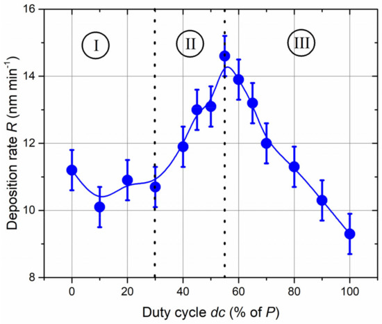
Figure 1.
Ti-B-N deposition rate (R) as a function of the duty cycle (dc) when a TiB2 target is RF-sputtered and nitrogen gas is injected with a pulsing period of P = 10 s. The deposition rate gradually changes, exhibiting a maximum dc close to 55% of P.
The evolution of deposition rate vs. duty cycle can be divided into three regions (I, II and III in Figure 1). For duty cycles lower than 30% of P (region I), a nearly constant rate can be assumed. The nitrogen injection time (less than 30% of P = 10 s) is too short for full nitriding of the TiB2 target surface. The boride sputtering mode prevails, and Ti-B-N films can be expected to exhibit characteristics similar to those of the TiB2 compound, i.e., metallic-like behavior. An increase in duty cycle from 30% to 55% of the pulsing period (P) (region II) gives rise to enhanced deposition rates from 10.7 to 14.6 nm min−1, respectively. The deposition rate exhibits a maximum for dc = 55% of P, and a further increase in duty cycle (region III) produces a continuous and linear drop in the deposition rate to 9.3 nm min−1 when the nitrogen gas is constantly supplied (i.e., for dc = 100% of P). For duty cycles lower than 55% of P, the nitrogen injection time (tON time) is too short to completely set the reactive sputtering process in the nitride mode. Alternations between nitride and boride modes occur during tON and tOFF times, respectively. Nitride mode prevails for duty cycles higher than 55% of P, and the TiB2 target surface becomes increasingly covered by a nitride compound, which reduces the sputtering yield. Similarly, nitrogen atoms are progressively incorporated into the Ti-B-N films as the nitrogen injection tON time is increased, corresponding to the formation of a poisoning nitride layer on the target surface and a decrease in the deposition rate. This optimized deposition rate vs. nitrogen injection corroborates with results previously reported by Chaleix and Machet [33] and later by Pierson et al. [34], who also obtained a maximum rate for a given range of nitrogen flow rates. Similarly, we assigned this maximum rate of nitrogen incorporation to the growing films and a progressive nitriding of the target leading to a decrease in the deposition rate (typical of minimally reactive systems).
3.1. Composition and Structure
The films composition as a function of the duty cycle was first determined from XPS analyses. XPS spectra show clear signals corresponding to Ti 2p, N 1s and B 1s peaks. (Figure 2).
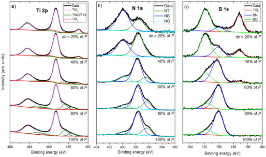
Figure 2.
XPS spectra of (a) Ti 2p, (b) N 1s and (c) B 1s of Ti-B-N thin films prepared with various duty cycles (dc).
The position of these peaks is in agreement with the results recorded by other investigators [35,36]. A curve fitting-procedure was systematically performed for all recorded signals and for various duty cycles. The Ti 2p peak consists of three components corresponding to the contributions from TiO2 (458.2 and 464.1 eV due to Ti 2p1/2 and Ti 2p3/2, respectively), TiNO/TiN (456.7 and 462.3 eV) and TiB2 (454.3 eV), as illustrated in Figure 2a. For the N 1s spectra (Figure 2b), decomposition leads to three contributions: NTi (396.9 eV), NB (398.3 eV) and NO (402.8 eV). The B 1s spectra also display three contributions assigned to TiB2 (187.8 eV), BN (190.0 eV) and BO (192.1 eV).
For the 2p levels of titanium (Figure 2a), the decomposition is more complicated. The contributions of TiO2 are still visible at 458.2 and 464.1 eV due to Ti 2p1/2 and Ti 2p3/2, respectively. The main difficulty is associated with determining the contributions of TiN/TiNO on the one hand and those of TiB2 on the other hand. For each of these compounds, the forms are complex and cannot be reduced to a simple component. Moreover, because pure standards of TiN and TiB2 compounds are not accurately produced, the best prepared samples were the TiN sample with 54% nitrogen and 46% titanium with no boron detected and a sample as close as possible to TiB2 with 58% boron, 34% titanium and 8% nitrogen (atomic concentrations). The maximum of intensity was at 456.7 eV for TiNO/TiN and at 454.3 eV for TiB2.
For the lowest duty cycles and up to dc = 40% of P, curve fitting of Ti 2p and B 1s peaks gives rise to signals corresponding to Ti–B bonds with TiB2 peak at 454 eV and 187 eV, as shown in Figure 2a,c. As expected, a significant contribution of film oxidation is measured from Ti–O and B–O bonds with TiO2 peaks at 458 and 464 eV (2p1/2 and 2p3/2 signals in Figure 2a), as well as with BO peak at 192 eV (Figure 2c). As the duty cycle increases (dc = 60% of P and higher), the TiB2 contribution recorded from the Ti 2p and B 1s peaks reduces and vanishes for a constant supply of nitrogen. Similarly, the BN peak from N 1s (398 eV) and B 1s (190 eV) becomes increasingly intense, as well as the TiN peak at 396 eV (Figure 2b). The film oxidation remains for any duty cycle, but it mainly originates from Ti signals (high reactivity of this metal towards oxygen), with a significant reduction in the influence of B–O and N–O bonds, as reflected by NO and BO peaks at 400 eV (Figure 2b) and 192 eV (Figure 2c), respectively. As expected, increasing the duty cycle from 0 to 100% of P favors the amount of Ti-N and B-N bonds, whereas that of Ti–B bonds decreases without completely preventing film oxidation due to the high reactivity between titanium and oxygen.
[Ti], [B] and [N] atomic concentrations in the films as a function of duty cycle (neglecting the amount of oxygen due to surface oxidation) were determined based on Ti 2p, N 1s and B 1s signals (Figure 3).
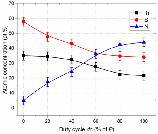
Figure 3.
[Ti], [B] and [N] atomic concentrations vs. duty cycle (dc) obtained from XPS measurements.
These three elemental concentrations exhibit a continuous and smooth variation with increased nitrogen injection time. B and N concentrations show a reverse evolution, whereas the Ti concentration slightly reduces (note that concentrations were determined assuming homogeneous compositions through the film thickness, which is not completely relevant and induces an assumed inaccuracy of ±3 at.% for the chemical concentration). Without nitrogen pulsing (dc = 0% of P), the [B]/[Ti] atomic concentration ratio is close to 1.8, which is lower than that of the stoichiometric TiB2 compound due to the presence of oxygen (more than 10 at.%) and a few at.% of nitrogen. When nitrogen is constantly injected (dc = 100% of P), nitrogen-rich Ti-B-N films are prepared with [N] content of more than 44 at.% and [B] content of approximately 35 at.%. For duty cycles higher than 60% of P, the three element concentrations tend to stabilize. The reverse evolution of nitrogen and boron contents vs. nitrogen supply is in agreement with results previously reported by Pierson et al. [37] and Han et al. [38], who also sputter-deposited Ti-B-N films from a TiB2 target in an Ar + N2 atmosphere. WE also observed the same kind of saturation for Ti, B and N atomic concentrations as the nitrogen flow rate increased (stabilization of the concentrations for nitrogen injections depending on the operating conditions).
The composition of the films is plotted within the Ti-B-N ternary phase diagram (Figure 4).
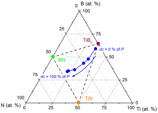
Figure 4.
The composition of Ti-B-N films (blue symbols) sputter-deposited by pulsing the nitrogen gas from dc = 0 to 100% of the pulsing period of P = 10 s within a ternary phase diagram. The positions of TiB2, TiN and BN stoichiometric compounds are indicated, as well as quasi-binary tie lines between the individual compounds (dashed lines).
TiB2, TiN and BN stoichiometric compounds are indicated, as well as quasi-binary tie lines between the individual compounds (dashed lines). Nitrogen pulsing does not produce a chemical composition evolution along the quasi-binary TiN-TiB2 line, as reported for Ti-B-N films prepared by PACVD [39]. Instead, it moves away from such a line as the duty cycle increases with a BN enrichment of the films, as the nitrogen supply tends to be constant. This trend was previously reported by others [40,41], giving rise to a comparable saturation of nitrogen content in the Ti-B-N films, even by sputtering a TiB2 target in a pure nitrogen atmosphere. At first, as proposed by Mayrhofer et al. [42], we suggest the formation of a composite structure composed of TiN and TiB2 nanocrystals randomly distributed in the film and embedded into a disordered and amorphous a-BNx compound. Assuming this nanocrystalline Ti-B-N structure, the corresponding phase proportions (mole fractions) are 42% TiN, 10% TiB2 and 48% BN in the equilibrium phase diagram for Ti-B-N films prepared with dc = 100% of P. As expected, reducing the duty cycle leads to reduced contents of TiN and BN phases (e.g., for dc = 40% of P, phase proportions in mole fractions are 28% TiN, 53% TiB2 and 19% BN). Furthermore, the use of a short nitrogen injection time (dc = 20% of P) leads to a significant incorporation of N in Ti-B-N films due to the high reactivity of nitrogen towards titanium and boron elements.
The occurrence of chemical bonds can be highlighted by FTIR analyses, especially for light elements, such as B and N. Figure 5 shows the FTIR spectra recorded for Ti-B-N films deposited on (100) silicon and for various duty cycles. No clear signals are recorded for duty cycles lower than 45% of P. Some peaks appear as the nitrogen injection time increases and become more significant when the duty cycle exceeds 55% of P. A broad asymmetric band appears close to 1390 cm−1 and clearly develops as dc reaches 90% of P, which is mainly assigned to the characteristic absorption of hexagonal BN (in-plane B-N bond stretching) in a Ti-B-N single layer [43,44].
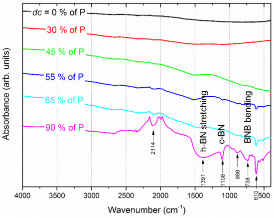
Figure 5.
FTIR spectra measured for Ti-B-N films prepared by pulsing nitrogen gas with an increasing duty cycle from 0 to 90% of the pulsing period of P = 10 s.
Similarly, a broad and significant signal is measured around 738 cm−1 related to the B-N-B bending mode occurring in the amorphous boron nitride [37], and a second signal is associated with the transverse optical mode of the cubic BN phase at 1108 cm−1 [45,46]. A narrow and intense peak can also be noticed at 610 cm−1, with a few weak peaks between 500 and 600 cm−1. This group of signals corresponds to Ti-N bonds (typical stretching mode of TiN around 600 cm−1 [47]). All these FTIR signals support the formation and increasing amount of B-N and Ti-N bonds for high duty cycles, maintaining an amorphous film structure. These results are in agreement with X-ray diffraction analyses results in which no diffraction peaks were detected due to boron nitride or other phases (not shown here).
3.2. Electrical Properties
The DC electrical resistivity of Ti-B-N thin films deposited on glass at room temperature (ρ300K) continuously rises as a function of the duty cycle, spanning more than six orders of magnitude as dc changes from 0 to 100% of P (Figure 6). Because the nitrogen pulsing period is very short (P = 10 s) and as a result of variation in deposition rates from 9.3 to 14.6 nm min−1 (Figure 1), a random N and B distribution is first produced through the film thickness rather than a multilayered structure, which could influence electrical conductivity, as previously reported for metal/metal oxide coatings [48]. For a dc lower than 40% of P, the resistivity is in the range of typical metals, i.e., below 10−5 Ω m. Afterwards, Ti-B-N films abruptly become more resistive for duty cycles between 40 and 80% of P and tend to stabilize to a few Ω m as nitrogen gas is constantly supplied. Carrier mobility (µ300K) and carrier concentration (n300K) at 300 K are also both influenced by the nitrogen injection for a similar range of duty cycles. The carrier concentration is more than 1028 m−3 for films prepared with duty cycles of less than 40% of P, typically corresponding to metallic-like behaviors. The carrier concentration loses several orders of magnitude as the duty cycle changes from 60 to 100% of P, where n300K = 2.9 × 10¹⁹ m−3. Similarly, the carrier mobility exhibits a reverse evolution with µ300K lower than a few 10−4 m2 V−1 s−1 for the lowest duty cycles, whereas it reaches 2.0 × 10⁻² m2 V−1 s−1 for dc = 100% of P. As a result, this drop in conductivity is mainly assigned to the strong decrease in the free carrier concentration, which prevails with enhanced mobility. These significant variations in electronic transport properties of Ti-B-N films correlate with their nitrogen enrichment and thus with an increasing amount of amorphous BN phase. These results support conclusions previously reported by Rogl [18], who claimed that metallic-like behavior can be expected for boron-rich compounds but that with increasing nitrogen content, semiconducting insulating properties can be expected to develop.
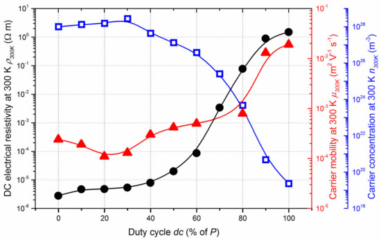
Figure 6.
DC electrical resistivity (ρ300K), carrier mobility (µ300K) and carrier concentration (n300K) measured at room temperature as a function of the duty cycle (dc) of Ti-B-N thin films.
Moreover, this abrupt increase in resistivity obtained for duty cycles between 40 and 80% of P also corresponds to the transition from absorbent (metallic-like) to transparent (semiconducting-like) Ti-B-N films in the visible region (optical transmittance spectra of Ti-B-N films deposited on glass not shown here).
The relationship of resistivity vs. temperature also supports this gradual metal-to-semiconducting transition as the duty cycle and thus the nitrogen content in Ti-B-N films increases (Figure 7). A nearly temperature-independent resistivity can be noticed for the lowest duty cycles, where ρ is maintained nearly constant from 30 to 200 °C, with, for example, a negative temperature coefficient of resistance at 300 K (TCR300K) of −8.6 × 10⁻⁵ K−1 for films prepared without nitrogen pulsing. This is consistent with the results reported by Pierson et al. [49], who also reported negative TCR values and the loss of metallic character, even for Ti-B-N films prepared with low nitrogen flow rates. Their results also showed a significant increase in TiBN electrical resistance for a given range of nitrogen flow rates corresponding to negative TCRs, which is, in some ways similar, to the sudden increase in resistivity measured for duty cycles higher than 40% of P (Figure 6). In our TiBN films, TCR300K becomes even more negative for dc = 50% of P, with TCR300K =−3.9 × 10⁻⁴ K−1, and a further increase in the nitrogen injection time leads to a semiconducting-like behavior, with an exponential decrease in the film resistivity as the temperature rises. An Arrhenius plot (electrical conductivity vs. reciprocal temperature) gives rise to an activation energy of Ea = 12 meV for dc = 60% of P, reaching 124 meV for a constant supply of nitrogen flow rate (dc = 100% of P). This increasing activation energy is connected to the nitrogen enrichment of Ti-B-N films, as well as to the formation of an amorphous and insulating BN phase. However, the highest value of activation energy is quite low compared to typical semiconducting materials, although it remains in the order of magnitude of some nitride or boride semiconductors, for which the temperature-dependent resistivity strongly depends on their composition [50].
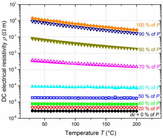
Figure 7.
DC electrical resistivity (ρ) vs. temperature (T) measured on Ti-B-N thin films deposited on glass for various duty cycles (dc = 0 to 100% of the constant pulsing period of P = 10 s).
Our results clearly show that electronic transport characteristics of Ti-B-N films progressively but rapidly change from metallic to semiconducting behaviors as a function of the duty cycle, in direct association with variations in composition and structure. At first and as frequently modeled for Ti-B-N mechanical properties, we can suppose that films exhibit a nanocomposite structure [39,42,51]. The latter is made of nanometric TiN and TiB2 crystallites (conductive phase) embedded in a disordered BN matrix (insulating medium).
Based on the sudden change in electrical properties of Ti-B-N films for a given range of duty cycles (Figure 6) and assuming a nanocomposite structure, a percolation model was used to describe the evolution of thin film conductivity at 300 K (σ300K) as a function of 1-ndc, where ndc is defined as the normalized duty cycle (Figure 8). Sputtering conditions with 1-ndc = 0 correspond to the most N-rich Ti-B-N films (i.e., dc = 100% of P) and therefore the most resistive films. Conductivity abruptly increases when 1-ndc reaches 0.4, and then tends to saturate. This σ300K vs. 1-ndc evolution typically behaves like a percolation phenomenon. Two electrically distinct media (insulating amorphous BN matrix and conducting TiN and TiB2 phases) are mixed in Ti-B-N films. The proportion of the conducting phase increases with increasing 1-ndc. As a result, the insulating–conducting transition corresponds to the percolation threshold, which can be determined assuming an effective medium theory (EMT) [52]. The percolation theory allows for description of the electrical conductivity of a composite medium before and after the percolation threshold (ϕc) through the following equations [53]:
before the percolation threshold (i.e., ϕ < ϕc), where σ = σ300K is the DC electrical conductivity at 300 K (S m−1), σi is the DC electrical conductivity of the insulating medium (S m−1), ϕ = 1-ndc is the conducting phase ratio (arb. units) and s is the critical exponent in the insulating region.
after the percolation threshold (i.e., ϕ > ϕc), where σc is the DC electrical conductivity of the conducting phase (S m−1), and t is the critical exponent in the conducting region.
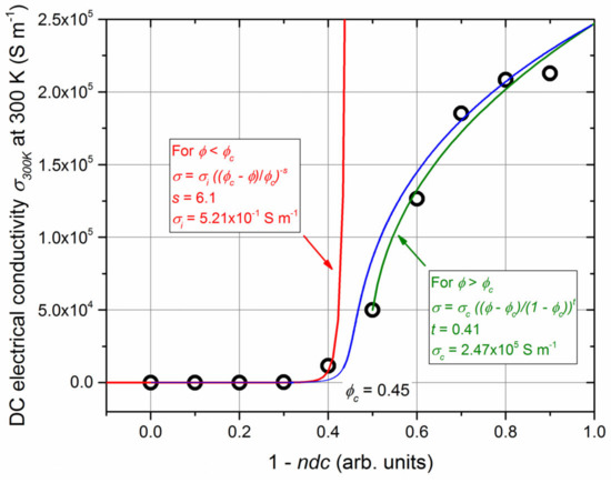
Figure 8.
DC electrical conductivity at room temperature (σ300K) vs. ϕ = 1-ndc for Ti-B-N thin films (ndc is the normalized duty cycle). Red and green lines are related to the conductivity calculated from the fitting before (Equation (1)) and after (Equation (2)) the percolation threshold. The blue line is the best fit obtained from Equation (3).
For the full range of conducting phase ratios (ϕ), a phenomenological relationship, can be used, as suggested by McLachlan et al. [54]:
with .
The best fittings were performed from these equations, as shown in Figure 8 (red and green lines for Equations (1) and (2), respectively). A percolation threshold of ϕc = 0.45 was obtained, which corresponds to dc = 55% of P. Based on the chemical compositions determined from XPS analyses (Figure 3), this duty cycle produced comparable B and N concentrations in Ti-B-N films. This result supports Mayrhofer et al., who claimed that this range of compositions matches with a film composed of two nanoscale phases (2–3 nm) encapsulated by a high-volume fraction (about 50%) of a disordered phase [38,41].
According to the experimental data at ϕ = 1, the conductivity of the conducting phase is σc = 2.47 × 10⁵ S m−1. This value is lower than that of single TiN and TiB2 films (σTiN = 1.85 × 10⁶ S m−1 [55] and σTiB2 = 3.52 × 10⁶ S m−1 [56]), as the conducting phase certainly contains defects and is composed of small grains (a few nm), although it remains in the order of magnitude of metallic materials. With respect to the insulating medium, results of the fits yield σi = 5.21 × 10⁻¹ S m−1. This value is higher than conductivities usually reported for BN compounds (σ is below 10−6 S m−1 for pure c-BN at room temperature [57]). This difference is understandable, as the electronic transport properties of BN strongly depend on crystallinity, preparation method, and the nature and type of doping [57]. In our Ti-B-N films, the insulating matrix certainly contains a significant amount of defects and Ti, favoring mobility and the concentration of free carriers, thus enhancing the overall conductivity.
Critical exponents s and t are also of interest, and universal values between sun = 0.7–1 and tun = 1.6–2 are commonly reported for three-dimensional systems with an inverse Swiss cheese model [52]. For our Ti-B-N films, fittings from experimental data lead to s = 6.1 and t = 0.41, which different significantly from universal values. These discrepancies can be assigned to an inhomogeneous structure of the films (percolation theory is based on perfect spherical particles for both insulating and conducting media). Sputtering deposition at room temperature often leads to columnar architectures [58], and RGPP may produce periodic multilayers [59]. As a result, our Ti-B-N films can be considered an anisotropic system affecting the percolation law, as the assumed homogeneity and sphericity of media are not fully established. However, fitting with Equation (3) and using parameters obtained from each region allows for a reliable description of the electrical conductivity of Ti-B-N films for the full range of duty cycles (blue line in Figure 8). This two-exponent phenomenological percolation equation can be used to assess the complex DC electrical conductivity of Ti-B-N films exhibiting reverse B and N concentrations.
4. Conclusions
In this study, 300 nm thick Ti-B-N thin films were sputter-deposited by RF reactive sputtering. A TiB2 target was sputtered in a reactive atmosphere composed of Ar and N2 gases. A reactive gas pulsing process (RGPP) was implemented to inject nitrogen gas with a constant pulsing period of P = 10 s. The duty cycle (dc) was systematically varied (tON injection time) in order to tune the chemical composition of the films. Nitrogen enrichment was achieved as the dc gradually increased from 0 to 100% of P. In the same way, the boron concentration was inversely reduced, maintaining a nearly constant Ti content. Furthermore, increasing the nitrogen injection time favored the occurrence of B-N bonds in the films, with a phase proportion close to 48% of BN (mole fraction) when nitrogen was constantly supplied (dc = 100% of P).
For duty cycles between 40% and 80% of P, electronic transport properties measured at room temperature significantly changed, with a resistivity enhancement of four orders of magnitude, whereas carrier mobility and concentration correspondingly changed for the same range of dc. A regular but rapid transition from metallic to semiconducting-like behavior was highlighted as a function of the duty cycle, as supported by the resistivity vs. temperature measurements. Assuming a nanocomposite structure in Ti-B-N films made of nanometric TiN and TiB2 crystallites (conductive phase) embedded in a disordered BN matrix (insulating medium), a percolation model adequately describes the conductivity of the tunable films as a function of nitrogen injection.
These results demonstrate that the proposed nanocomposite structure for mechanical properties and wear resistance of Ti-B-N films can also be applied to describe the electrical properties of such films as a function of B and N concentrations. Furthermore, our results indicate that the RGPP technique is a suitable approach to adjust electronic transport properties by means of a simple and easy change in pulsing parameters. A further incorporation of nitrogen in films would be relevant to further extend multiphase nanostructuring growth.
Author Contributions
Conceptualization and data curation, C.S.; methodology and software, J.-M.C.; formal analysis and validation, J.G.; formal analysis and validation, J.-Y.R.; formal analysis and validation, P.-H.C.; data curation and investigation, A.K.; formal analysis and validation, O.H.; writing—review and editing and funding acquisition, N.M. All authors have read and agreed to the published version of the manuscript.
Funding
This research was partially funded by Fonds Européen de Développement Régional—FEDER (grant number CTE 6059) in the framework of the TOOLEXPERT Interreg V project.
Institutional Review Board Statement
Not applicable.
Informed Consent Statement
Not applicable.
Data Availability Statement
All data are presented in the current manuscript.
Acknowledgments
This work was supported by the Région Bourgogne Franche-Comté and by EIPHI Graduate School (contract ‘ANR-17-EURE-0002’).
Conflicts of Interest
The authors declare no conflict of interest. The funders had no role in the design of the study; in the collection, analyses or interpretation of data; in the writing of the manuscript; or in the decision to publish the results.
References
- McManus-Driscoll, J.L.; Zerrer, P.; Wang, H.; Yang, H.; Yoon, J.; Fouchet, A.; Yu, R.; Blamire, M.G.; Jia, Q. Strain and spontaneous phase ordering in vertical nanocomposite heteroepitaxial thin films. Nature Mater. 2008, 7, 314–320. [Google Scholar] [CrossRef]
- Chen, A.; Bi, Z.; Jia, Q.; MacManus-Driscoll, J.L.; Wang, H. Microstructure, vertical strain control and tunable functionality in self-assembled vertically aligned nanocomposite thin films. Acta Mater. 2013, 61, 2783–2792. [Google Scholar] [CrossRef]
- Wu, J.F.; Yu, L.H.; Hu, H.B.; Asempah, I.; Xu, J.H. Structural, mechanical and tribological properties of NbCN-Ag nanocomposite films deposited by reactive magnetron sputtering. Coatings 2018, 8, 50. [Google Scholar] [CrossRef]
- Lopez, D.A.S.; Chagas, L.G.; Batista, A.D.; Guaita, M.G.D.; Amorin, L.H.C.; Da Silva, P.R.C.; Yamashini, G.; Zaia, D.A.M.; De Santana, H.; Urbano, A. Effect of RF magnetron sputtering parameters on the optimization of the discharge capacity of ternary lithium oxide thin films. J. Mater. Sci. 2021, 32, 17462–17472. [Google Scholar] [CrossRef]
- Txintxurreta, J.; G-Berasategui, E.; Ortiz, R.; Hernandez, O.; Mendizabal, L.; Barriga, J. Indium oxide thin film deposition by magnetron sputtering at room temperature for the manufacturing of efficient transparent heaters. Coatings 2021, 11, 92. [Google Scholar] [CrossRef]
- Saikumar, A.K.; Sundaresh, S.; Nehate, S.D.; Sundaram, K.B. Properties of RF magnetron sputtered copper gallium oxide (CuGa2O4) thin films. Coatings 2021, 11, 921. [Google Scholar] [CrossRef]
- Rebholz, C.; Leyland, A.; Schneider, J.M.; Voevodin, A.A.; Matthews, A. Structure, hardness and mechanical properties of magnetron-sputtered titanium-aluminium boride thin films. Surf. Coat. Technol. 1999, 120, 412–417. [Google Scholar] [CrossRef]
- Minemoto, T.; Negami, T.; Nishiwaki, S.; Takakura, H.; Hamakawa, Y. Preparation of Zn1-xMgxO films by radio frequency magnetron sputtering. Thin Solid Films 2000, 372, 173–176. [Google Scholar] [CrossRef]
- Greczynski, G.; Lu, J.; Jensen, J.; Bolz, S.; Kolker, W.; Schiffers, C.; Lemmer, O.; Greene, J.E.; Hultman, L. A review of metal-ion-flux-controlled growth of metastable TiAlN by HIPIMS/DCMS co-sputtering. Surf. Coat. Technol. 2014, 257, 15–25. [Google Scholar] [CrossRef]
- Palmquist, J.P.; Birch, J.; Jansson, U. Deposition of epitaxial ternary metal carbide films. Thin Solid Films 2002, 405, 122–128. [Google Scholar] [CrossRef]
- Glynn, C.; Aureau, D.; Collins, G.; O’Hanlon, S.; Etcheberry, A.; O’Dwyer, C. Solution processable broadband transparent mixed metal oxide nanofilm optical coatings via substrate diffusion doping. Nanoscale 2015, 7, 20227–20237. [Google Scholar] [CrossRef] [PubMed]
- Steinecke, M.; Kiedrowski, K.; Jupé, M.; Ristau, D. Very thick mixture oxide ion beam sputtering films for investigation of nonlinear material properties. Eur. Phys. J. Appl. Phys. 2017, 80, 30301–30305. [Google Scholar] [CrossRef]
- Martin, N.; Banakh, O.; Santo, A.M.E.; Springer, S.; Sanjinès, R.; Takadoum, J.; Lévy, F. Correlation between processing and properties of TiOxNy thin films sputter deposited by the reactive gas pulsing technique. Appl. Surf. Sci. 2001, 185, 123–133. [Google Scholar] [CrossRef]
- Vaz, F.; Cerqueira, P.; Rebouta, L.; Nascimento, S.M.C.; Alves, E.; Goudeau, P.; Rivière, J.P.; Pischow, K.; de Rijk, J. Structural, optical and mechanical properties of coloured TiNxOy thin films. Thin Solid Films 2004, 447, 449–454. [Google Scholar] [CrossRef]
- Fernandes, A.C.; Carvalho, P.; Vaz, F.; Lancero-Mendez, S.; Machado, A.V.; Parreira, N.M.G.; Pierson, J.F.; Martin, N. Property change in multifunctional TiCxOy thin films: Effect of the O/Ti ratio. Thin Solid Films 2006, 515, 866–871. [Google Scholar] [CrossRef][Green Version]
- Sanchez-Lopez, J.C.; Abad, M.D.; Carvalho, I.; Galindo, R.E.; Benito, N.; Ribeiro, S.; Henriques, M.; Cavaleiro, A.; Carvalho, S. Influence of silver content on the tribomechanical behavior on Ag-TiCN bioactive coatings. Surf. Coat. Technol. 2012, 206, 2192–2198. [Google Scholar] [CrossRef]
- Ji, A.L.; Ma, L.B.; Liu, C.; Li, C.R.; Cao, Z.X. Synthesis and characterization of superhard aluminum carbonitride thin films. Diam. Relat. Mater. 2005, 14, 1348–1352. [Google Scholar] [CrossRef]
- Rogl, P. Materials science of ternary metal boron nitrides. Int. J. Inorg. Mater. 2001, 3, 201–209. [Google Scholar] [CrossRef]
- Lu, Y.H.; Zhou, Z.F.; Sit, P.; Shen, Y.G.; Li, K.Y.; Chen, H. X-ray photoelectron spectroscopy characterization of reactively sputtered Ti-B-N thin films. Surf. Coat. Technol. 2004, 187, 98–105. [Google Scholar] [CrossRef]
- Tian, C.X.; Wang, Z.S.; Zou, C.W.; Tang, X.S.; Xie, X.; Lie, S.Q.; Liang, F.; Li, Z.J.; Liu, Y.F.; Su, F.H. Ternary and quaternary TiBN and TiBCN nanocomposite coatings deposited by arc ion plating. Surf. Coat. Technol. 2019, 359, 445–450. [Google Scholar] [CrossRef]
- Lu, Y.H.; Shen, Y.G.; Li, K.Y. Nanostructured two-phase nc-TiN/a-(TiB2, BN) nanocomposite thin films. Appl. Surf. Sci. 2006, 253, 1631–1638. [Google Scholar] [CrossRef]
- Mayrhofer, P.H.; Willmann, H.; Mitterer, C. Recrystallization and grain growth of nanocomposite Ti-B-N coatings. Thin Solid Films 2003, 440, 174–179. [Google Scholar] [CrossRef]
- Aoudi, S.M.; Namavar, F.; Gorishnyy, T.Z.; Rohde, S.L. Characterization of TiBN films grown by ion beam assisted deposition. Surf. Coat. Technol. 2002, 160, 145–151. [Google Scholar] [CrossRef]
- Andrievski, R.A. Structure and properties of nanostructured boride/nitride materials. Int. J. Refract. Met. Hard Mater. 1999, 17, 153–155. [Google Scholar] [CrossRef]
- Mayrhofer, H.; Mitterer, C.; Clemens, H. Self-organized nanostructures in hard ceramic coatings. Adv. Eng. Mater. 2005, 7, 1071–1082. [Google Scholar] [CrossRef]
- Kainz, C.; Schalk, N.; Tkadletz, M.; Mitterer, C.; Czettl, C. The effect of B and C addition on microstructure and mechanical properties of TiN hard coatings grown by chemical vapor deposition. Thin Solid Films 2019, 688, 137283–8. [Google Scholar] [CrossRef]
- Zhou, S.Y.; Pelenovich, V.O.; Han, B.; Yousaf, M.I.; Yan, S.J.; Tian, C.X.; Fu, D.J. Effects of modulation period on microstructure, mechanical properties of TiBN/TiN nanomultilayered films deposited by multi arc ion plating. Vacuum 2016, 126, 34–40. [Google Scholar] [CrossRef]
- Asempah, I.; Xu, J.H.; Yu, L.H.; Luo, H.; Liu, J.L.; Yu, D.; Ding, N. The role of copper incorporation on the microstructure, mechanical and tribological properties of TiBN-Cu films by reactive magnetron sputtering. J. Alloy. Compd. 2019, 801, 112–122. [Google Scholar] [CrossRef]
- Cicek, H.; Baran, O.; Demirci, E.E.; Tahmasebian, M.; Totik, Y.; Efeoglu, I. The effect of nitrogen flow rate on TiBN coatings deposited on cold work tool steel. J. Adhes. Sci. Technol. 2014, 28, 1140–1148. [Google Scholar] [CrossRef]
- Martin, N.; Lintymer, J.; Gavoille, J.; Chappé, J.M.; Sthal, F.; Takadoum, J.; Vaz, F.; Rebouta, L. Reactive sputtering of TiOxNy coatings by the reactive gas pulsing process—Part I: Pattern and period of pulses. Surf. Coat. Technol. 2007, 201, 7720–7726. [Google Scholar] [CrossRef]
- El Mouatassim, A.; Pac, M.J.; Pailloux, F.; Amiard, G.; Henry, P.; Rousselot, C.; Eydi, D.; Tuilier, M.H.; Cabioc’h, T. On the possibility of synthesizing multilayered coatings in the (Ti, Al)N system by RGPP: A microstructural study, Surf. Coat. Technol. 2019, 374, 845–851. [Google Scholar] [CrossRef]
- Fairley, N.; Fernandez, V.; Richard-Plouet, M.; Guillot-Deudon, C.; Walton, J.; Smith, E.; Flahaut, D.; Greiner, M.; Biesinger, M.; Tougaard, S.; et al. Systematic and collaborative approach to problem solving using X-ray photoelectron spectroscopy. Applied Surface Sci. Adv. 2021, 5, 100112. [Google Scholar] [CrossRef]
- Chaleix, L.; Machet, J. Study of the composition and of the mechanical properties of TiBN films obtained by d c. magnetron sputtering. Surf. Coat. Technol. 1997, 91, 74–82. [Google Scholar] [CrossRef]
- Pierson, J.F.; Chapusot, V.; Billard, A.; Alnot, M.; Bauer, P. Characterisation of reactively sputtered of Ti-B-N and Ti-B-O coatings. Surf. Coat. Technol. 2002, 151–152, 526–530. [Google Scholar] [CrossRef]
- Holzschuh, H. Deposition of Ti-B-N (single and multilayer) and Zr-B-N coatings by chemical vapor deposition techniques on cutting tools. Thin Solid Films 2004, 469–470, 92–98. [Google Scholar] [CrossRef]
- Hahn, R.; Tymoszuk, A.; Wojcik, T.; Kirnbauer, A.; Kozak, T.; Capek, J.; Sauer, M.; Foelske, A.; Hunold, O.; Polcik, P.; et al. Phase formation and mechanical properties of reactively and non-reactively sputtered Ti-B-N hard coatings. Surf. Coat. Technol. 2021, 420, 127327. [Google Scholar] [CrossRef]
- Pierson, J.F.; Tomasella, E.; Bauer, P. Reactively sputtered Ti-B-N nanocomposite films: Correlation between structure and optical properties. Thin Solid Films 2002, 408, 26–32. [Google Scholar] [CrossRef]
- Han, B.; Neena, D.; Wang, Z.; Kondamareddy, K.K.; Li, N.; Zuo, W.; Yan, S.; Liu, C.; Fu, D. Investigation of structure and mechanical properties of plasma vapor deposited nanocomposite TiBN films. Plasma Sci. Technol. 2017, 19, 045503. [Google Scholar] [CrossRef]
- Mayrhofer, P.H.; Stoiber, M. Thermal stability of superhard Ti-B-N coatings. Surf. Coat. Technol. 2007, 201, 6148–6153. [Google Scholar] [CrossRef]
- Lin, J.; Moore, J.J.; Mishra, B.; Pinkas, M.; Sproul, W.D. The structure and mechanical and tribological properties of TiBCN nanocomposite coatings. Acta Mater. 2010, 58, 1554–1564. [Google Scholar] [CrossRef]
- Karuna Purnapu Rupa, P.; Chakraborti, P.C.; Mishra, S.K. Structure and indentation behavior of nanocomposite Ti-B-N films. Thin Solid Films 2014, 564, 160–169. [Google Scholar] [CrossRef]
- Mayrhofer, P.H.; Mitterer, C.; Wen, J.G.; Petrov, I.; Greene, J.E. Thermally induced self-hardening of nanocrystalline Ti-B-N thin films. J. Appl. Phys. 2006, 100, 044301. [Google Scholar] [CrossRef]
- Chu, K.; Shen, Y.G. Mechanical and tribological properties of nanostructured TiN/TiBN multilayer films. Wear 2008, 265, 516–524. [Google Scholar] [CrossRef]
- Tsai, P.C. The deposition of characterization of BCN films by cathodic arc plasma evaporation. Surf. Coat. Technol. 2007, 201, 5108–5113. [Google Scholar] [CrossRef]
- Kurooka, S.; Ikeda, T.; Kohama, K.; Tanaka, T.; Tanaka, A. Formation and characterization of BN films with Ti added. Surf. Coat. Technol. 2003, 166, 111–116. [Google Scholar] [CrossRef]
- Moreno, H.; Caicedo, J.C.; Amaya, C.; Munoz-Saldana, J.; Yate, L.; Esteve, J.; Prieto, P. Enhancement of surface mechanical properties by using TiN/[BCN/BN]n/c-BN multilayer system. Appl. Surf. Sci. 2010, 257, 1098–11104. [Google Scholar] [CrossRef]
- Sedira, S.; Achour, S.; Avci, A.; Eskizeybek, V. Physical deposition of carbon doped titanium nitride film by DC magnetron sputtering for metallic implant coating use. Appl. Surf. Sci. 2014, 295, 81–85. [Google Scholar] [CrossRef]
- Cacucci, A.; Tsiaoussi, I.; Potin, V.; Imhoff, L.; Martin, N.; Nyberg, T. The interdependence of structural and electrical properties in TiO2/TiO/Ti periodic multilayers. Acta Mater. 2013, 61, 4215–4225. [Google Scholar] [CrossRef][Green Version]
- Pierson, J.F.; Bertran, F.; Bauer, J.P.; Jolly, J. Structural and electrical properties of sputtered titanium boronitride films. Surf. Coat. Technol. 2001, 142–144, 906–910. [Google Scholar] [CrossRef]
- Wang, C.C.; Akbar, S.A.; Chen, W.; Patton, V.D. Electrical properties of high-temperature oxides, borides, carbides and nitrides. J. Mater. Sci. 1995, 30, 1627–1641. [Google Scholar] [CrossRef]
- Mitterer, C.; Mayrhofer, P.H.; Beschliesser, M.; Losbichler, P.; Warbichler, P.; Hover, F.; Gibson, P.N.; Gissler, W.; Hruby, H.; Musil, J.; et al. Microstructure and properties of nancomposite Ti-B-N and Ti-B-C coatings. Surf. Coat. Technol. 1999, 120–121, 405–411. [Google Scholar] [CrossRef]
- Nan, C.W. Physics of inhomogeneous inorganic materials. Progr. Mater. Sci. 1993, 37, 1–116. [Google Scholar] [CrossRef]
- Fabreguette, F.; Maglione, M.; Imhoff, L.; Domenichini, B.; Marco de Lucas, M.C.; Sibillot, P.; Bourgeois, S.; Sacilotti, M. Conductimetry and impedance spectroscopy study of low pressure metal organic chemical vapor deposition TiNxOy films as a function of the growth temperature: A percolation approach. Appl. Surf. Sci. 2001, 175–176, 574–578. [Google Scholar] [CrossRef]
- McLachlan, D.S.; Cai, K.; Sauti, G. AC and DC conductivity-based microstructural characterization. Int. J. Refract. Met. Hard Mater. 2001, 19, 437–445. [Google Scholar] [CrossRef]
- Liang, H.; Xu, J.; Zhou, D.; Sun, X.; Chu, S.; Bai, Y. Thickness dependent microstructural and electrical properties of TiN thin films prepared by DC reactive magnetron sputtering. Ceram. Int. 2016, 42, 2642–2647. [Google Scholar] [CrossRef]
- Raman, M.; Wang, C.C.; Chen, W.; Akbar, S.A. Electrical resistivity of titanium diboride and zirconium diboride. J. Am. Ceram. Soc. 1995, 78, 1380–1382. [Google Scholar] [CrossRef]
- Zhang, X.W. Doping and electrical properties of cubic boron nitride thin films: A critical review. Thin Solid Films 2013, 544, 2–12. [Google Scholar] [CrossRef]
- Anders, A. A structure zone diagram including plasma-based deposition and ion etching. Thin Solid Films 2010, 518, 4087–4090. [Google Scholar] [CrossRef]
- Zaoui, M.; Bourceret, A.; Gaillard, Y.; Giljean, S.; Rousselot, C.; Pac, M.J.; Richard, F. Relation between hardness of (Ti, Al)N based multilayered coatings and periods of their stacking. Acta Polytech. 2020, 27, 79–83. [Google Scholar] [CrossRef]
Publisher’s Note: MDPI stays neutral with regard to jurisdictional claims in published maps and institutional affiliations. |
© 2022 by the authors. Licensee MDPI, Basel, Switzerland. This article is an open access article distributed under the terms and conditions of the Creative Commons Attribution (CC BY) license (https://creativecommons.org/licenses/by/4.0/).