Article

Design and Research of Laminated Packaging Structure for Semiconductor Laser Diode

1
School of science, Changchun University of Science and Technology, Changchun 130022, China
2
The 34th Institute of China Electronics and Technology Group Corporation, Guilin 541000, China
*
Author to whom correspondence should be addressed.
Coatings 2022, 12(10), 1450; https://doi.org/10.3390/coatings12101450
Submission received: 5 September 2022 / Revised: 21 September 2022 / Accepted: 27 September 2022 / Published: 1 October 2022

Abstract

:
The primary factor influencing semiconductor laser performance is photoelectric conversion efficiency. In this study, a heat sink structure in the form of a laminated DC-mount package was created using Solidworks 2018 in accordance with the semiconductor laser C-mount packaging structure specifications. The Workbench 17.0 program theoretically derived the link between the device’s junction temperature and power, and then optimized the size of its heat sink. The primary characteristics of semiconductor laser devices with various C-type and DC-type heat sink architectures were then packaged and compared. Results demonstrate that thermal resistance decreased by 31%, the power of the semiconductor laser device with a DC packaging structure increased by 0.5 W, and photoelectric conversion efficiency increased to over 60%, thereby lowering the temperature at the device junction and thermal resistance. at least to a certain point. the effect of the parasitic parameters of the package is effectively improved. Finally, the 3000 h life test confirmed this package construction’s stability.

1. Introduction

High-powered semiconductor lasers are widely used in the entire optoelectronics field, including laser processing, 3D printing, LIDAR, and military and medical applications, due to their brightness, reliability, good coherence, and small size, which allows for easy integration. As a result of the significant potential of semiconductor lasers, the demand for packaging technology, which is closely related to their performance, is increasing. At present, the packaging of single-tube semiconductor laser chips mainly adopts the single-sided flip-fit lamination method, which has been continuously improved and optimized. However, due to its heat sink volume, material, and other factors, the extent to which this packaging form’s photoelectric conversion efficiency can be enhanced is limited, which restricts the working performance of semiconductor lasers [1,2,3].
Nozaki et al. proposed a new dual thermal flow packaging technique for InGaN semiconductor lasers using a ceramic carrier constructed of double-layer group III nitride for packaging, which can achieve high power as well as high temperature operation. This structure effectively reduces the device’s thermal resistance and achieves an output power of 3 W at 85 °C and 1.9 W at 140 °C [4]. Zhang et al. proposed a vertical package structure, sandwiching the chip in the heatsink, and compared the device’s junction temperature and power with the traditional structure using ANSYS finite element analysis; results showed that the new package structure had lower thermal resistance and higher output power [5]. Wang et al. proposed a semiconductor laser package structure using double-sided lamination cooling and a chip with a cavity length of 4 mm and a strip width of 100 μm; through simulation and experimentation, and finally double-sided packaging, the device’s maximum temperature was reduced from 48.5 °C to 40 °C, and its maximum power was increased from 14.1 W to 15.1 W at an operating current of 20 A [6].
In semiconductor laser work, after cooling the equipment to achieve heat dissipation, heat is dissipated by the active light-emitting area of the semiconductor laser’s chip along the lower side of the laminated heat sink. However, this heat dissipation method is relatively simple, the heat flow density per area unit is high, and the heat surge affects the photoelectric conversion efficiency of the device. Therefore, the group designed a double-sided DC-mount (hereinafter referred to as DC-type) package structure using Solidworks 2018 and Workbench 17.0. This new structure effectively protects the laser chip, and has double-sided heat dissipation performance, which can effectively increase the heat dissipation area of the semiconductor laser chip. In a laser performance comparison analysis with the traditional C-mount type (hereinafter referred to as C-type) package structure, this new DC-type structure had a higher heat dissipation effect and efficiency, effectively reduced the device’s thermal resistance and junction temperature, reduced wavelength red shift, and improved the device’s photoelectric conversion efficiency [7,8].

2. Structure Design and Thermal Analysis

In practice, the key dimensions of the C-type structure have been widely used in the structural parameters of various related devices; any change in the dimensions of parameters (such as the center hole’s position, light output height, and thickness) will affect the normal application of the device. Therefore, we designed the double C-mount (DC-mount) package structure by improving and optimizing the traditional C-type structure using the same dimensions.

2.1. Structural Modeling

Solidworks is a 3D modeling mechanical drawing software (version 2018); it can design 3D models and assembly, and effectively analyze the structures of required parts, dimensions, and other related parameters. After modeling the heat sink structure in 3D using Solidworks 2018 and considering the electrical interconnection of the device’s structure, error accuracy, and gold wire bonding position, the traditional C-type package structure and the new DC package structure were designed using the heat sink structure shown in the Figure 1.
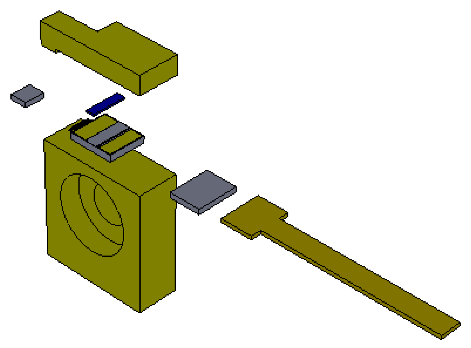
An expanded view of the DC-type structure after modeling is shown in Figure 2 below.

2.2. Heat Transfer

When a semiconductor laser operates, internal heat conduction occurs; heat is not transferred on the isothermal plane, but along the direction normal to the isothermal plane. In the temperature field, the temperature gradient is a vector quantity that represents the rate of change in the temperature at any point along the direction normal to the isotherm, and the direction of temperature increase is usually taken as the positive direction of the temperature gradient.
Heat per area unit per time unit is a proportional function of the spatial rate of change in temperature along the direction, i.e., [9]
q = k u x
where the negative sign indicates the temperature from high to low, is the heat flow density (W/m2), and is the heat conduction coefficient [W/(m·°C)].
In heat conduction, for a 3D isotropic medium there are [10,11]:
q x = k u x , q y = k u y , q z = k u z
It can be derived that:
q ( x , y , z ) = k ( x , y , z ) u ( x , y , z )
as the 3D active non-simultaneous heat conduction equation (isotropic).
u t a 2 ( 2 u x 2 + 2 u y 2 + 2 u z 2 ) = f ( x , y , z , t )
where a 2 = k c ρ , f = F ( x , y , z , t ) c ρ , f is a non-simultaneous term, c is the specific heat capacity (J/kg·°C), ρ is the density of the medium (kg/m3), F ( x , y , z , t ) is the amount of heat generated per unit of time per unit of volume.
u t a 2 ( 2 u x 2 + 2 u y 2 + 2 u z 2 ) = 0
is a 3D heat transfer equation without heat source flush (isotropic).

2.3. Thermal Design Analysis

In the first analysis of the relationship between the sizes of the two types of packaged heat sink structures and the devices’ junction temperatures, the impact of thermal stress on performance was not considered, because semiconductor laser chip properties and heat sink material properties (such as the coefficient of thermal expansion, creep resistance, Young’s modulus, and Poisson’s ratio) are somewhat different. In laser work, the heat surge will lead to a certain degree of deformation between the two; the resulting stress leads to a shortened working life of the semiconductor laser, the spectrum appears double-peaked, multi-peaked, and other phenomena occur. However, most lasers in the packaging (through the packaging’s first level), use the thermal expansion coefficient and other related parameters to match the secondary heat sink for the transition. In addition, the application of a reasonable thickness of solder and mis-temperature packaging, etc., can effectively reduce the generation of stress. Single tube and bar semiconductor lasers are different; there is no “Smile” effect, and thermal stress has less impact on the performance of the former [12,13].
In addition, considering that the size and shape of each layer of this package structure’s heat sink are different, it is impossible to find an analytical solution for the heat dispersion equation. If the thermal size of each layer is regarded as the same, the result will deviate from the analytical solution. Therefore, the dimensional optimization analysis of the heat sink was carried out using finite elements.
The method of thermal analysis in the finite element analysis was to reduce the problem of solving differential equations to a numerical calculation with a finite number of cells by dividing the modeled part into a finite number of “cells” and connecting each cell with a node. This was followed by setting material parameters and applying different parameters to each material part according to the type of analysis required, and finally solving and setting conditions for the final finite element analysis solution.
According to the model established above, conditions were imported into ANSYS Workbench 17.0 for steady-state thermal analysis.
First, material properties (engineering data) were defined; as the material of various structures were different, the thermal conductivity and other parameters were also different. Table 1 lists the relevant parameters of the structural materials required for the device [14].
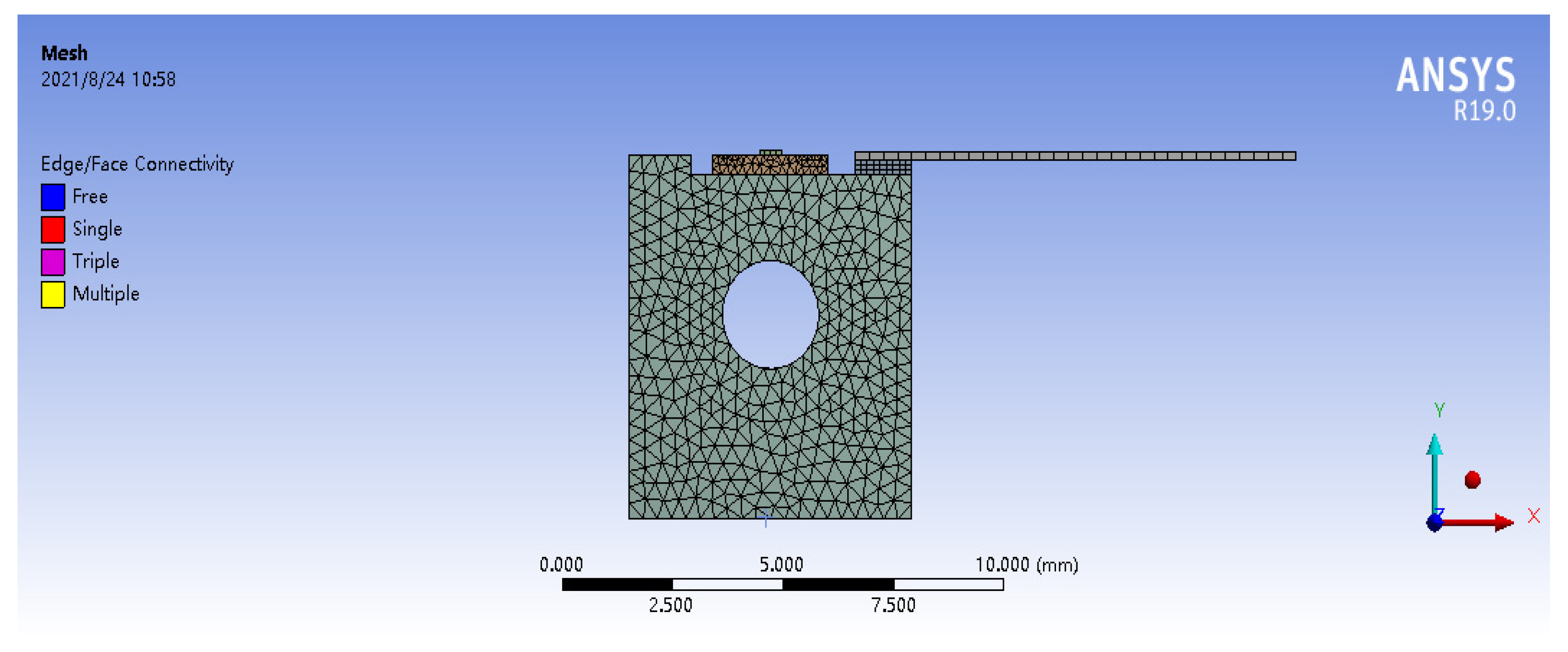
After setting the material’s parameters, the model was pre-processed; i.e., meshed (using Mesh). When meshing a model, the mesh should be densely divided in regions of large temperature variation, especially in the chip, to ensure the accuracy of temperature variation in the simulation as well as the clarity of observations [15]. The model’s meshing is shown in the Figure 3.
Next, loading conditions, including heat flux, heat flow rate, and internal heat generation, were applied to facilitate analysis during the finite element simulation.
The photoelectric conversion efficiency of the semiconductor laser was considered to be 50%; i.e., when the laser was working, half of the energy was converted to heat. In the operating state, the thermal conductivity of each structural material does not change with temperature; in actual operation, the bottom of the heat sink was in contact with the water-cooling device and TEC equipment, and its temperature was considered to be room temperature, i.e., 25 °C [16].
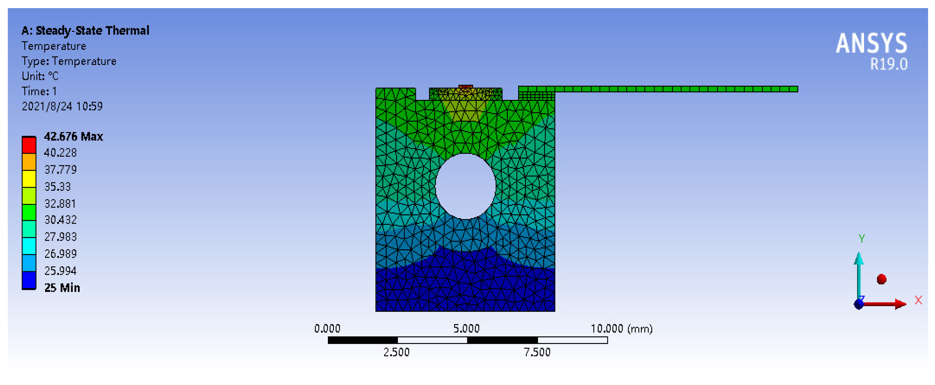
Finally, all conditions of the finite element analysis were set; the temperature distribution cloud of the device after solving (Solve) is shown in the following Figure 4. The temperature unit for all values in the following graphs is °C.
Temperature variation patterns and distributions of the semiconductor laser under normal operation were observed using finite element analysis. Notably, heat generated by the laser during operation was conducted out through the heat sink. However, the heat sink volume affected its temperature conduction rate and the junction temperature of the device; the size of the upper side heat sink structure was analyzed to optimize the heat sink structure.
Diagrams of the device’s junction temperatures corresponding to different heat sink structure sizes are shown in Figure 5, where “Thickness” is the overall thickness of the upper side heat sink; when “Thickness = 0” it is regarded as a C-type heat sink structure.
In summary, the device’s junction temperature was lowest at 1.5 mm; i.e., when the thickness of the upper side heat sink was 1.5 mm. According to the definition of thermal resistance in heat transfer, when the thickness of the heat sink reaches a certain value, the thermal diffusion angle reaches the maximum, the thermal resistance value is the minimum, and the heat flow density value is the lowest; this is why the thickest upper side heat sink did not have the best the thermal performance [17,18].
Finally, by applying the loading condition described in 2.3. above, device junction temperature simulations and heat vector variation analyses were performed for the C-type and DC-type structures with optimized heat sink size; the temperature distribution clouds for both structures at an output power of 5 W are shown in Figure 6a,b.
As can be seen in Figure 7, when the semiconductor laser was operating stably, the junction temperature of the device in its C-type package structure was 44.809 °C, and the junction temperature of the device in the DC-type package structure was 35.288 °C. The junction temperature decreased by 9.521 °C, or approximately 21.2%. The new package structure reduced the device’s junction temperature to a certain extent.
The heat vector distribution diagrams of the two package structures are shown in Figure 7a,b. These diagrams illustrate that, compared to the C-type package structure, the DC-type package structure had bi-directional heat dissipation which increased the heat dissipation range of the laser chip and effectively reduced the heat flow density of the device. This improved the heat dissipation capability of the laser and enhanced the working performance of the semiconductor laser.

2.4. Junction Temperature vs. Power

The junction temperatures of devices with different package structures derived from the above finite element analysis vary, according to Equation [19]:
T j = T h s + R t h ( I V P o u t )
where, T j is the device junction temperature, T h s is the heat sink temperature, R t h is the device thermal resistance, I is the input current, V is the input voltage, and P o u t is the output optical power. This leads to:
R t h = T j T h s I V P o u t
In addition, the threshold current, I t h , can be expressed by the following relation [20]:
I t h = I R e T T R T 0
where T 0 is the characteristic temperature of the device, T R is the reference temperature of the device, and I R is the threshold current of the device at the reference temperature. The slope efficiency η can be expressed as:
η = η R e - ( T T R T 1 )
where η R is the slope efficiency of the device at the reference temperature T R , and T 1 is the characteristic temperature of the device.
According to the expression for output power:
P out = η ( I I t h )
Finally, in the above expression, the relationship between the device’s output power and the device’s junction temperature can be deduced as:
P o u t = η R e ( T T R T 1 ) ( I I R e T T R T 0 )
From the above equation, it can be seen that for a given semiconductor laser, T 1 and T 0 are constant values, and the device’s junction temperature value is the key factor affecting the output power.
In summary, the characteristics of the new DC heat sink structure were initially investigated by modeling its design and finite element simulation analysis, optimizing the size of the heat sink structure and comparing the results of the analysis, and concluding that the junction temperature of the device was a factor affecting the output power through relevant theoretical equations. The following experimental comparison of the two structures was carried out to verify the accuracy and reliability of the above design and analysis.

3. Experimental Verification

In this experiment, we used the same size laser chip and two heat sink structures as described above in the finite element analysis; the single-tube semiconductor laser with InGaAs/GaAs material and 5 W output power, 808 nm wavelength, 200 μm chip’s width and 2000 μm chip’s cavity length was used as the experimental object. AuSn solder was used for the primary package (die-bonding) and In solder was used for the secondary package (reflow soldering). To ensure the accuracy of the experiment, a consistent laser chip, the same size solder, and the same package process parameters were used for the experiment. The laser chip was packaged in two structures, C-type and DC-type, and finally bonded by gold wire; the prepared package structures are shown in the Figure 8.
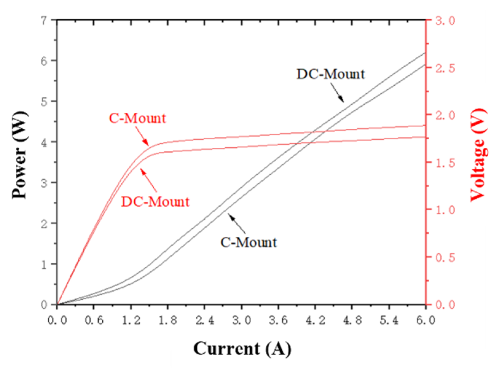
The typical P-I characteristics of the two prepared devices were tested; the comparative P-I characteristics curves of the semiconductor lasers in the two package structures are shown in the Figure 9.
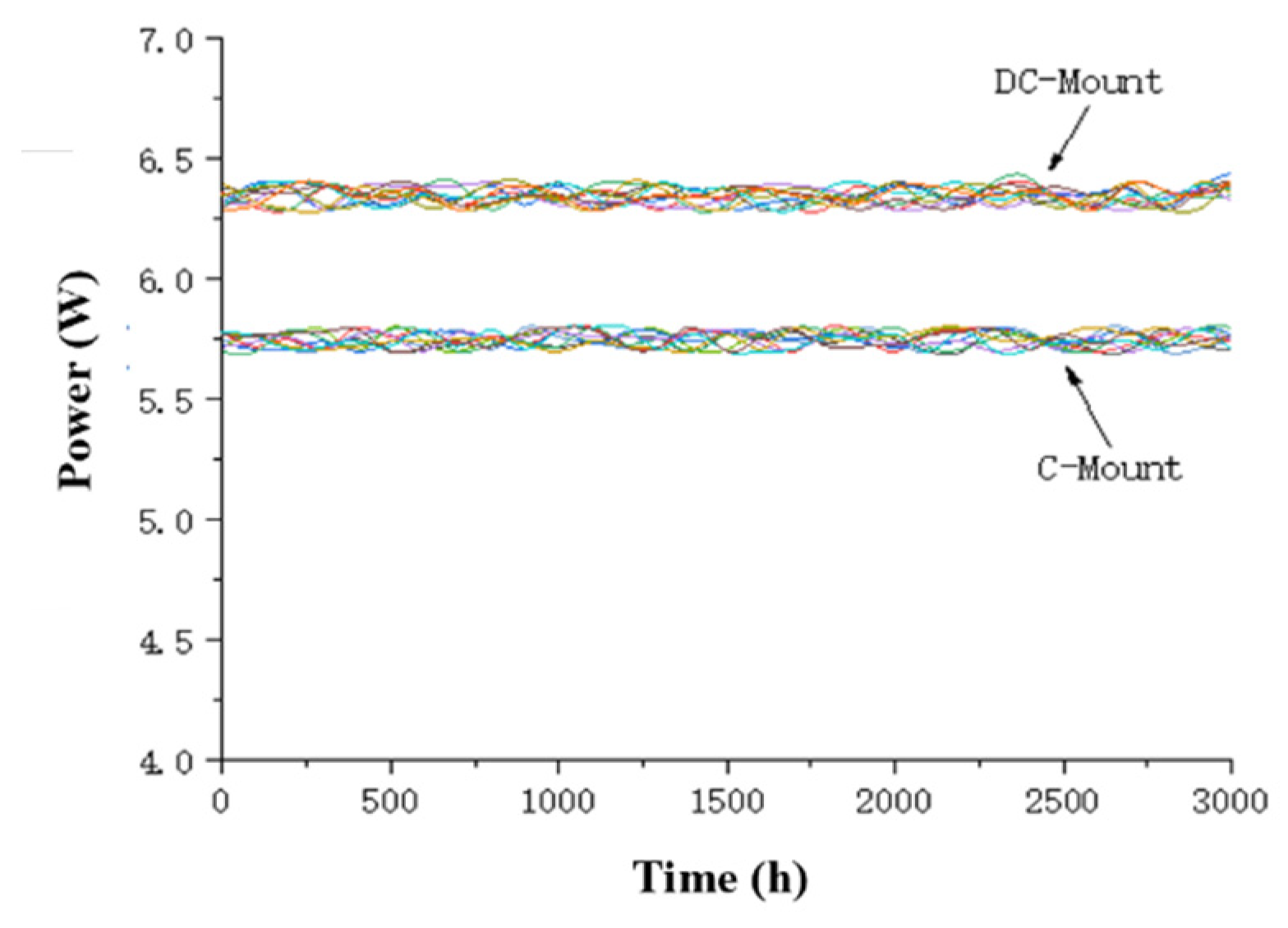
Comparing the typical parameter values of both devices in CW condition (6 A), the threshold current Ith of the semiconductor laser decreased from 0.78 A to 0.56 A, the photoelectric conversion efficiency increased from 53.22% to 60.20%, the junction voltage decreased from 1.86 V to 1.73 V, and the device’s power increased by approximately 8.6%. Measuring the junction temperatures of the devices illustrated that the thermal resistance decreased. Finally, ten devices with each of the two structures were selected for 3000 h life tests (shown in Figure 10; no defective devices were detected.
In addition, the DC-type package structure improved the laser’s response characteristics to a certain extent; it allowed the gold wire bonding between the chip and the transition heat sink to be dispensed with, reducing the number of gold wires, which effectively reduced the chip parasitic effect and the package’s parasitic parameters [21].
Finally, the device was tested under vibration, shock, and high and low temperature conditions with no adverse phenomena. Although the C-mount package structure of the semiconductor laser is relatively mature and widely applied, the new device can be operated at a lower drive current and can meet higher experimental and production requirements, effectively improving the device’s performance.

4. Conclusions

In this experiment, a stacked package structure (DC-mount), based on the C-type package structure of semiconductor lasers, was designed using Solidworks 2018 and Workbench 17.0. Heat sink size optimization was carried out based on the theory of heat conduction analysis, and the relationship between junction temperature and the device’s power was theoretically derived, providing a certain theoretical basis for the subsequent experimental validation. The relevant parameters of the prepared C-type and DC-type packages for semiconductor lasers were tested and compared by designing precise fixtures, selecting materials, and preparing two sets of semiconductor laser devices according to the relevant packaging technology. Results show that the DC-type had a lower threshold current, 0.5 W higher optical power, 60% higher photoelectric conversion efficiency, and 31% lower junction temperature, which are superior across all parameters. Finally, the 3000 h life test results indicated that the device’s performance was good, which indirectly verified the reliability of the semiconductor laser in this package structure. At present, the devices are still in the process of aging. This DC-type package structure for semiconductor lasers can significantly increase the power of the pump source; in the same operating conditions, the device has excellent parameters and performance.

Author Contributions

Writing—original draft and investigation, P.X. and Y.Q.; data analysis and derived formula, B.W.; funding acquision, Y.T. and X.W.; experiment set up and data analysis guidance, Y.W. All authors have read and agreed to the published version of the manuscript.

Funding

This research was funded by the Jilin Scientific and Technological Development Program (No. 20160203017GX); Jilin Provincial Department of Education Scientific Research Project (No. JJKH20220750KJ).

Institutional Review Board Statement

Not applicable.

Informed Consent Statement

Not applicable.

Data Availability Statement

Not applicable.

Conflicts of Interest

The authors declare no conflict of interest.

References

  1. Yan, Y.; Zheng, Y.; Sun, H.; Duan, J. Review of Issues and Solutions in High-Power Semiconductor Laser Packaging Technology. Front. Phys. 2021, 9, 669591. [Google Scholar] [CrossRef]
  2. Wandera, C.; Kujanpää, V.; Salminen, A. Laser power requirement for cutting thick-section steel and effects of processing parameters on mild steel cut quality. Proc. Inst. Mech. Eng. Part B J. Eng. Manuf. 2011, 225, 651–661. [Google Scholar] [CrossRef]
  3. Bachmann, F. Goals and Status of the German National Research Initiative. Proc. SPIE 2007, 6456, 1–12. [Google Scholar]
  4. Nozaki, S.; Yoshida, S.; Yamanaka, K.; Imafuji, O.; Takigawa, S.; Katayama, T.; Tanaka, T. High-power and high-temperature operation of an InGaN laser over 3 W at 85 °C using a novel double-heat-flow packaging technology. Jpn. J. Appl. Phys. 2016, 55, 04EH05. [Google Scholar] [CrossRef]
  5. Zhang, X.; Bo, B.; Qiao, Z.; Xu, Y.; Gao, X. Analysis of thermal characteristics based on a new type diode laser packaging structure. Opt. Eng. 2017, 56, 085105. [Google Scholar] [CrossRef]
  6. Wang, Y.; Qu, H.; Zheng, W. Study on New Type of Double-Sided Cooling Packaging Technology for Semiconductor Lasers. IOP Conf. Ser. Earth Environ. Sci. 2021, 769, 042003. [Google Scholar] [CrossRef]
  7. Ni, Y.; Jing, H.; Kong, J.; Wang, C.; Liu, S.; Ma, X. Thermal Performance of High-Power Laser Diodes Packaged by SiC Ceramic Submount. Chin. J. Lasers 2018, 45, 0101002. [Google Scholar] [CrossRef]
  8. Faircloth, B.O. High-brightness high-power fiber coupled diode laser system for material processing and laser pumping. Proc. SPIE 2003, 4973, 34–41. [Google Scholar]
  9. England, P.C.; Bruce, T.A. Pressure—Temperature—Time Paths of Regional Metamorphism I. Heat Transfer during the Evolution of Regions of Thickened Continental Crust. J. Petrol. 1984, 25, 894–928. [Google Scholar] [CrossRef]
  10. Sadeghipour, M.S.; Manzari, M. Finite element solution of the non-Fourier heat conduction equation. HTD - Am. Soc. Mech. Eng. Heat Transf. Div. 1990, 130, 141–148. [Google Scholar]
  11. Wang, B.L.; Han, J.C. A finite element method for non-Fourier heat conduction in strong thermal shock environments. Front. Mater. Sci. China 2010, 4, 226–233. [Google Scholar] [CrossRef]
  12. Wang, J.; Shi, L.; Li, Y.; Jin, L.; Xu, Y.; Zhang, H.; Zou, Y.; Lan, Y.; Ma, X. Thermal management of graphene-induced high-power semiconductor laser package with bidirectional conduction structure. Opt. Laser Technol. 2021, 139, 106927. [Google Scholar] [CrossRef]
  13. Liu, X.; Zhao, W.; Xiong, L.; Liu, H. Packaging of High-Power Semiconductor Lasers; Springer: New York, NY, USA, 2015. [Google Scholar]
  14. Liu, V.X. Technology Trend and Challenges in High Power Semiconductor Laser Packaging. In Proceedings of the 2010 IEEE Electronic Components & Technology Conference, Las Vegas, NV, USA, 1–4 June 2010. [Google Scholar]
  15. Ma, Z.; Lin, T.; Zhao, R.; Sun, W.; Mu, Y.; Li, Y.; Xie, J. Research on Thermal Analysis Modeling of Semiconductor Laser Based on Package Prototype. Laser Optoelectron. Prog. 2021, 58, 9. [Google Scholar]
  16. Lorenzen, D.; Hennig, P. Highly Thermally Conductive Substrates with Adjustable CTE for Diode Laser Bar Packaging; International Society for Optics and Photonics: Bellingham, WA, USA, 2003. [Google Scholar]
  17. Wu, D.H.; Zah, C.E.; Liu, X. Three-dimensional thermal model of a high-power diode laser bar. Appl. Opt. 2018, 57, 9868–9876. [Google Scholar] [CrossRef] [PubMed]
  18. Vermeersch, B.; Mey, G.D. Influence of substrate thickness on thermal impedance of microelectronic structures. Microelectron. Reliab. 2007, 47, 437–443. [Google Scholar] [CrossRef] [Green Version]
  19. Coldren, L.A.; Corzine, S.W.; Mashanovitch, M.L. Diode Lasers and Photonic Integrated Circuits. Opt. Eng. 1997, 55–60. [Google Scholar] [CrossRef]
  20. Bacchin, G.; Fily, A.; Qiu, B.; Fraser, D.; Robertson, S.; Loyo-Maldonado, V.; McDougall, S.D.; Schmidt, B. High temperature and high peak-power 808 nm QCW bars and stacks. Proc. SPIE 2010, 7583, 75830P. [Google Scholar]
  21. Zhu, N. Microwave Design and Characterization of Optoelectronic Devices and Packaging; Chinese Science Publishing & Media Ltd.: Beijing, China, 2007. (In Chinese) [Google Scholar]
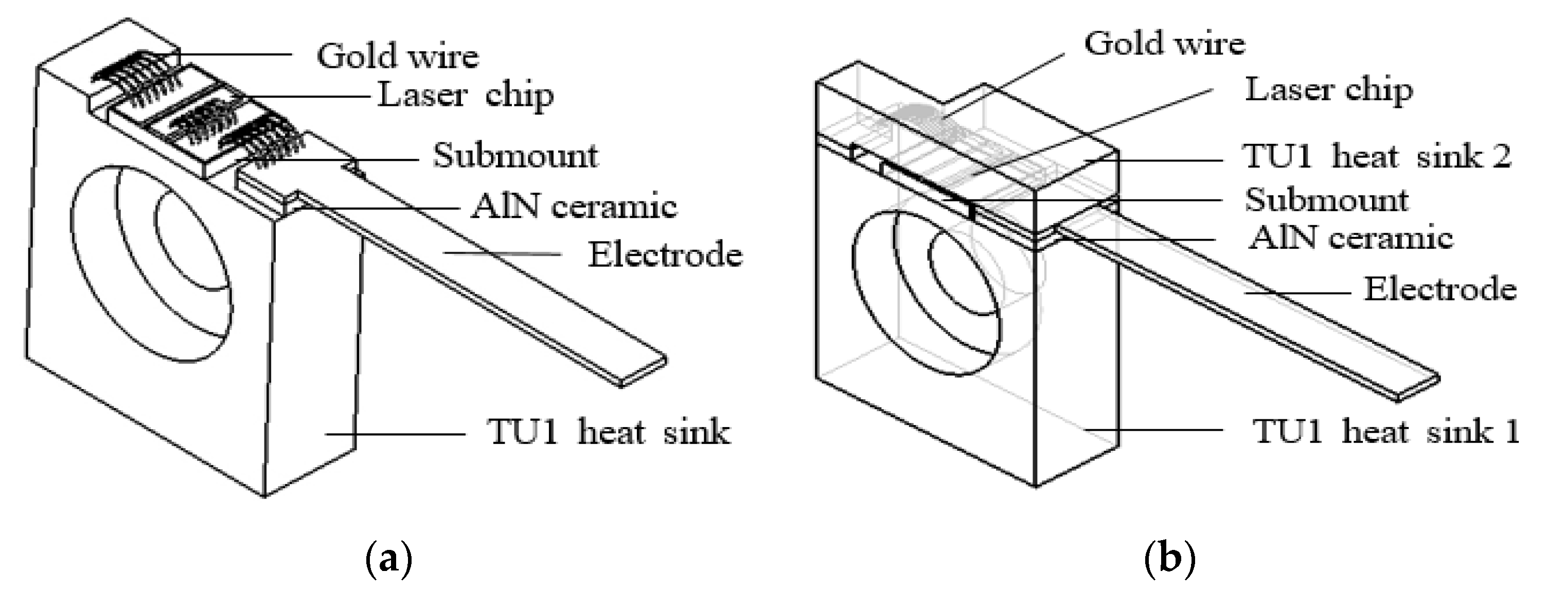
Figure 1. C-type and DC-type package structure diagrams. (a) C-type package structure and (b) DC-type package structure.
Coatings 12 01450 g001
Figure 2. The 3D expanded view of the DC-type structure.
Coatings 12 01450 g002
Figure 3. Mesh division diagram.
Coatings 12 01450 g003
Figure 4. Cloud map of temperature distribution.
Coatings 12 01450 g004
Figure 5. Comparison of thermal analyses of different heat sink sizes.
Coatings 12 01450 g005
Figure 6. C-type and DC-type package temperature distribution diagrams. (a) C-type package temperature diagram and (b) DC-type package temperature diagram.
Coatings 12 01450 g006
Figure 7. C-type and DC-type package temperature vector diagrams. (a) C-type package temperature vector diagram and (b) DC-type package temperature vector diagram.
Coatings 12 01450 g007
Figure 8. C-type and DC-type package structure physical diagrams. (a) C-type package structure physical diagram and (b) DC-type package structure physical diagram.
Coatings 12 01450 g008
Figure 9. P-I-V characteristics comparison curve.
Coatings 12 01450 g009
Figure 10. Life test curve comparison.
Coatings 12 01450 g010
Table 1. Parameters related to the device’s structure materials.
StructureMaterialSize (L × W × H) (mm)Thermal Conductivity [W/(m·°C)]
Laser chipGaAs2 × 0.5 × 0.1255
AuSn filmAuSn2 × 0.5 × 0.0157.3
In filmIn2.6 × 2.2 × 0.0583.7
SubmountAlN2.6 × 2.2 × 0.4180
Heat sink 1TU16.4 × 2.4 × 7.3398
Heat sink 2TU16.4 × 2.4 × -398
Publisher’s Note: MDPI stays neutral with regard to jurisdictional claims in published maps and institutional affiliations.