Article

CuI/Spiro-OMeTAD Double-Layer Hole Transport Layer to Improve Photovoltaic Performance of Perovskite Solar Cells

Center of Condensed Matter and Material Physics, School of Physics, Beihang University, Beijing 100191, China
*
Author to whom correspondence should be addressed.
Coatings 2021, 11(8), 978; https://doi.org/10.3390/coatings11080978
Submission received: 19 July 2021 / Revised: 11 August 2021 / Accepted: 12 August 2021 / Published: 17 August 2021
(This article belongs to the Special Issue Advanced Perovskite Films for Photovoltaic Application)

Abstract

:
The hole transport layer (HTL) is one of the main factors affecting the efficiency and stability of perovskite solar cells (PSCs). However, obtaining HTLs with the desired properties through current preparation techniques remains a challenge. In the present study, we propose a new method which can be used to achieve a double-layer HTL, by inserting a CuI layer between the perovskite layer and Spiro-OMeTAD layer via a solution spin coating process. The CuI layer deposited on the surface of the perovskite film directly covers the rough perovskite surface, covering the surface defects of the perovskite, while a layer of CuI film avoids the defects caused by Spiro-OMetad pinholes. The double-layer HTLs improve roughness and reduce charge recombination of the Spiro-OMeTAD layer, thereby resulting in superior hole extraction capabilities and faster hole mobility. The CuI/Spiro-OMeTAD double-layer HTLs-based devices were prepared in N2 gloveboxes and obtained an optimized PCE (photoelectric conversion efficiency) of 17.44%. Furthermore, their stability was improved due to the barrier effect of the inorganic CuI layer on the entry of air and moisture into the perovskite layer. The results demonstrate that another deposited CuI film is a promising method for realizing high-performance and air-stable PSCs.

1. Introduction

Perovskite, an organic–inorganic metal halide, which acts as a light absorber for solid film solar cells, has attracted extensive attention lately as a result of its excellent photoelectric properties, such as direct band gap, low exciton binding energy, wide light absorption spectrum range, long electron/hole diffusion length and high absorption [1,2,3,4,5,6]. In just a few years, perovskite solar cell efficiency reached 25.5% [7,8]. In the process of fabricating PSCs, we use upright structure or inverted structure. The upright structure is deposited perovskite films on electronic transport materials (ETMs) on FTO substrates, while the inverted structure is composed of perovskite films deposited on HTM on FTO substrates [9,10]. In many related research studies, organic hole transport layers, including Spiro-OMeTAD, are the most commonly used in NIP structures [11,12,13,14]. Though Spiro-OMeTAD is the most popular, the Li-TFSI in acetonitrile corrodes perovskite film, resulting in a rough Spiro-OMeTAD film, and a large number of pinholes appear; through these pinholes the perovskite film contacts water and oxygen in the air directly [15].
In recent years, CuI, CuO, CuCrO2, NiOx, Cu2O and CuSCN have been used as hole transporting layers to improve device stability [16,17,18,19,20,21,22,23]. Vahid et al. introduced a new method of depositing CuI, using a CuI/Cu structure as a hole transport and buffer layer at the same time, to achieve a PCE of 9.24% [24]. Hong et al. inserted a p-type cesium (CS: NiOx) layer, which yielded an optimum efficiency of 19.24% [19]. Shao et al. improved the PCE to 16.47%, by coating NiOx nanoparticles on the surface of organic–inorganic hybrid perovskite solar cells without using any other post-treatment [25]. Chen et al. obtained 19.0% high steady state PCE of perovskite solar cells by low-temperature CuCrO nanocrystals as HTL [26]. The CuI Island modified TiO2 ETL in planar PSCs prepared by Park et al. obtained high efficiency, with the PCE of the planar PSCs reaching 19.0% [27]. Therefore, it can be concluded that CuI is a cheap, promising material. Yu et al. added CuSCN to CuI HTL, and the perovskite PCE was shown to reach 18.76%, which is higher than that of pure CuI (14.53%) and CuSCN (16.66%)-based perovskite solar cells [28]. Copper salt has good electrical conductivity, can be dissolved in solution, and has good stability. Doping is for the sake of combining Spiro levels with CuI stability. Inorganic salts prevent perovskite film decomposition to a certain extent. Zhang et al. prepared Spiro-OMeTAD doped with CuI (20% mol ratio), and it was shown that CuI could effectively oxidize Spiro-OMeTAD and obtain the best PCE of 12.8% [29]. However, the efficiency based on copper iodide is relatively low. In addition, experience has shown that the Spiro-OMeTAD layer contains many holes derived from lithium bis(trifluoromethanesulfonyl)imines (LiTFSI) dopants, and these pinholes are found between the perovskite layer and the air or electrode, thereby leading to a poor stability or efficiency. Few researchers inserted the CuI into the absorption layer and the transport layer as a buffer layer by solution spin coating, which is convenient and cost-effective. CuI is not.
Perovskite coating technology includes magnetron sputtering technology, ion diffusion, evaporation in specific environments, plasma enhanced atomic layer deposition (PEALD), high temperature coating and precursor spin coating technology. In view of the characteristics of perovskite thin film materials, in most cases, researchers use precursor technology and co-evaporation technology due to the fact that the cost of coating technology is relatively low compared with co-evaporation technology, and the precursor spin coating technology has the lowest cost, is easy to control, and the required environment and equipment are relatively simple. Most importantly, the control of the amount of solvent in the solution is relatively simple. Therefore, we chose solvent spin coating technology.
In this study, we applied CuI solution by dissolving copper iodide in 1:39 di-n-propyl to chlorobenzene. CuI has long been used as a hole transport layer because of its appropriate energy level, which is very suitable for perovskite solar cells. Additionally, we deposited the CuI next to the perovskite layer, on account of the Spiro-OMeTAD-layer, which does not require annealing. In order to resolve the existing pinholes, we considered the two CuI and Spiro-OMeTAD materials together, and prepared CuI/Spiro-OMeTAD-based double hole transporting layers. We successively spun CuI on perovskite and Spiro-OMeTAD on CuI, to form a double hole transport layer-based device. We demonstrated that the CuI layer was able to stop perovskite corrosion caused by acetonitrile from Spiro-OMeTAD solution. Therefore, it can improve efficiency to some extent. In addition, more matching of energy levels is conducive to hole extraction, which results in a better VOC (voltage of open circuit) and FF (fill factor). Finally, we achieved a 17.44% PCE for double HTLs based devices, and the VOC was 1.10 V, which was 0.05 V higher than a single Spiro-OMeTAD HTL based device. The stability of perovskite solar cells was thus further improved.

2. Materials and Methods

2.1. Cleaning Glass

First, we dealt the FTO (fluorine-doped tin oxide) (150 nm) substrate with detergent. Next it was washed with deionized water, followed by ultrasonic cleaning. We ultrasonic cleaned the FTO glass with absolute ethyl alcohol, isopropanol and acetone for 30 min, respectively. Lastly, we took out the FTO glass from the acetone and blow-dried it with N2, then placed it in an ozone processor for 30 min ozone treatment.

2.2. Preparation of the HTL Solution

72.3 mg of Spiro-OMeTAD, Li-TFSI (bistrifluoromethanesulfonimide lithium salt) solution, and 28.8 µL tBP mixed in 1 mL of chlorobenzene. Deposited at 4000 rpm for 30 s.

2.3. Preparation of the Perovskite Precursor Solution

1.1 M FAI (formamidine iodide), 1.1 M PbI2, 0.2 M MABr (methylazanium bromide) and 0.22 M PbBr2 and 1ml DMF:DMSO (4:1). Lastly, 52.6 mL CsI.

2.4. Fabrication

SnO2 was deposited on the FTO. SnO2 electron transport compact layer was deposited on FTO coated glass substrate by a two-step spin-coating process, first at the spin speed of 1500 rpm for 30 s, leading further to 2500 rpm for next 30 s for compact layer. The SnO2 film was finally annealed at 150 °C in air for 1 h. The Cs/MA/FA perovskite solution was spin-coated onto the SnO2 layer at 1000 rpm for 10 s, then at 3000 rpm for 20 s, and a chlorobenzene (CB) antisolvent was used in the last 10s to obtain a perovskite/SnO2/FTO substrate. These substrates were then heated to 100 °C for 60 min. Next, the hole transport layer Spiro-OMeTAD or CuI/spiro-OMeTAD was deposited on top of the Cs/MA/FA perovskite layer at 4000 rpm for 30 s. For CuI/Spiro-OMeTAD double hole transport layers, the perovskite film was first coated with CuI solution at 4000 rpm for 30 s, then annealed at 130 °C for 20 min and cooled. The CuI surface was then coated with a spiro-Meotad solution at 4000 rpm for 30 s. It was put in a drying oven for 12 h. Finally, the gold electrode was evaporated by hot evaporation.

2.5. Characterizations

The SEM images were observed by the FEI NOVA NANOSEM 450 cold field scanning electron microscope (FEI Company, Hillsboro, TX, USA). The atom force microscopy (AFM) (Thermomicroscopes, Sunnyvale, CA, USA) analysis of the Cs/MA/FA films, Cs/MA/FA/Spiro-MeOTADfilms and Cs/MA/FA/CuI/Spiro-MeOTAD films were obtained on a Dimension Icon. The roughness value, and images processing were taken on a NanoScope (Nanoscope V, Vecco) while the J-V plots of Cs/MA/FA/spiro-MeOTAD and Cs/MA/FA/CuI/Spiro-MeOTAD devices were characterized by Keithley 2400 Source in dark conditions, measured by an Agilent B1500A Semiconductor) (Abet Technologies, Milford, MA, USA). The PL spectra were recorded by an Edinburgh Instrument FLS920 (PICOQUANT, Berlin, Germany). The TRPL spectra were measured by an Edinburgh Instrument FLS920 (PICOQUANT, Berlin, Germany). The space-charge limited current (SCLC) and EIS were obtained using a multi-channel potentiostat (Biologic, Paris, France).

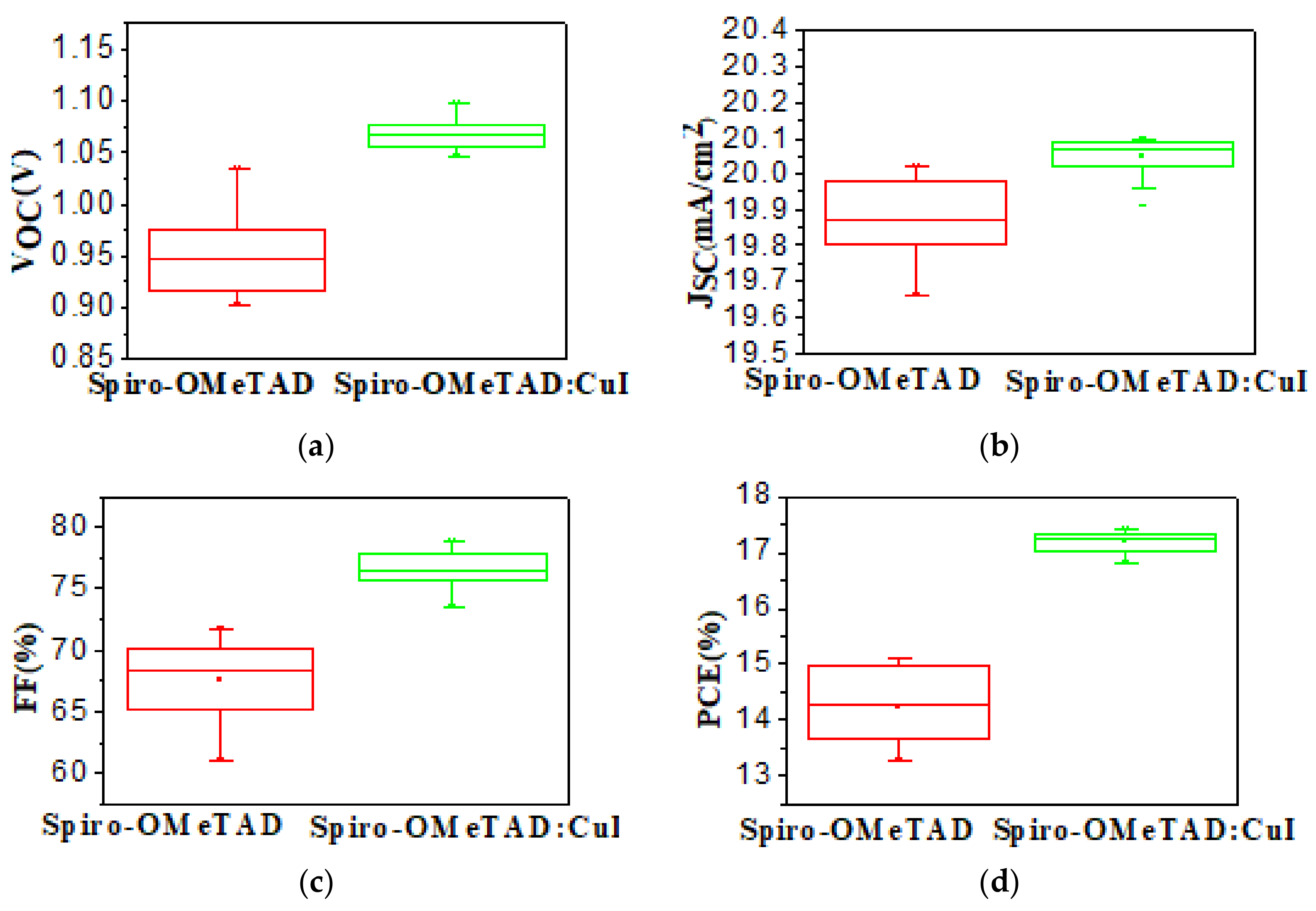
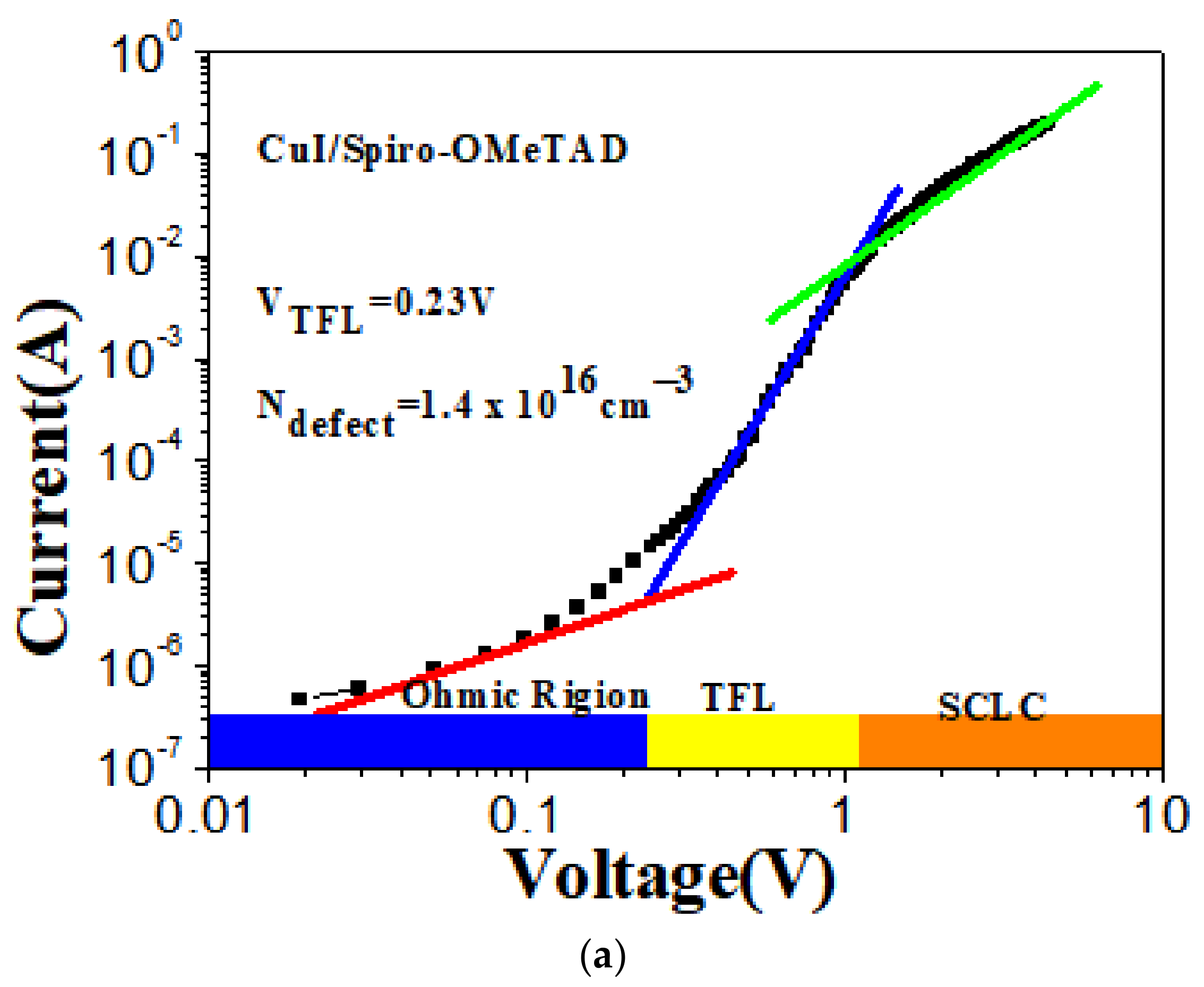
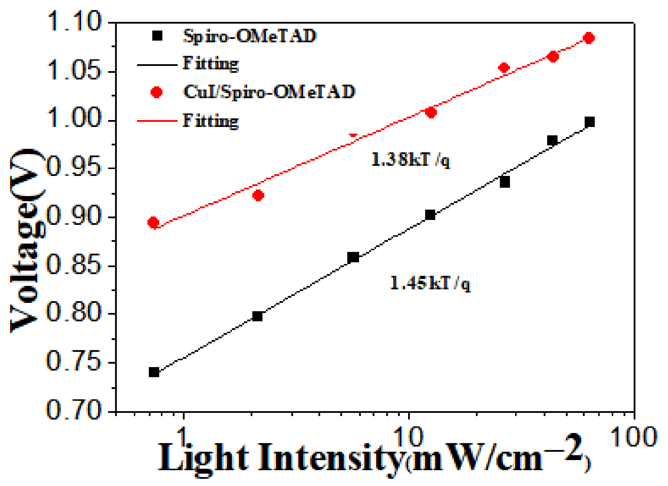
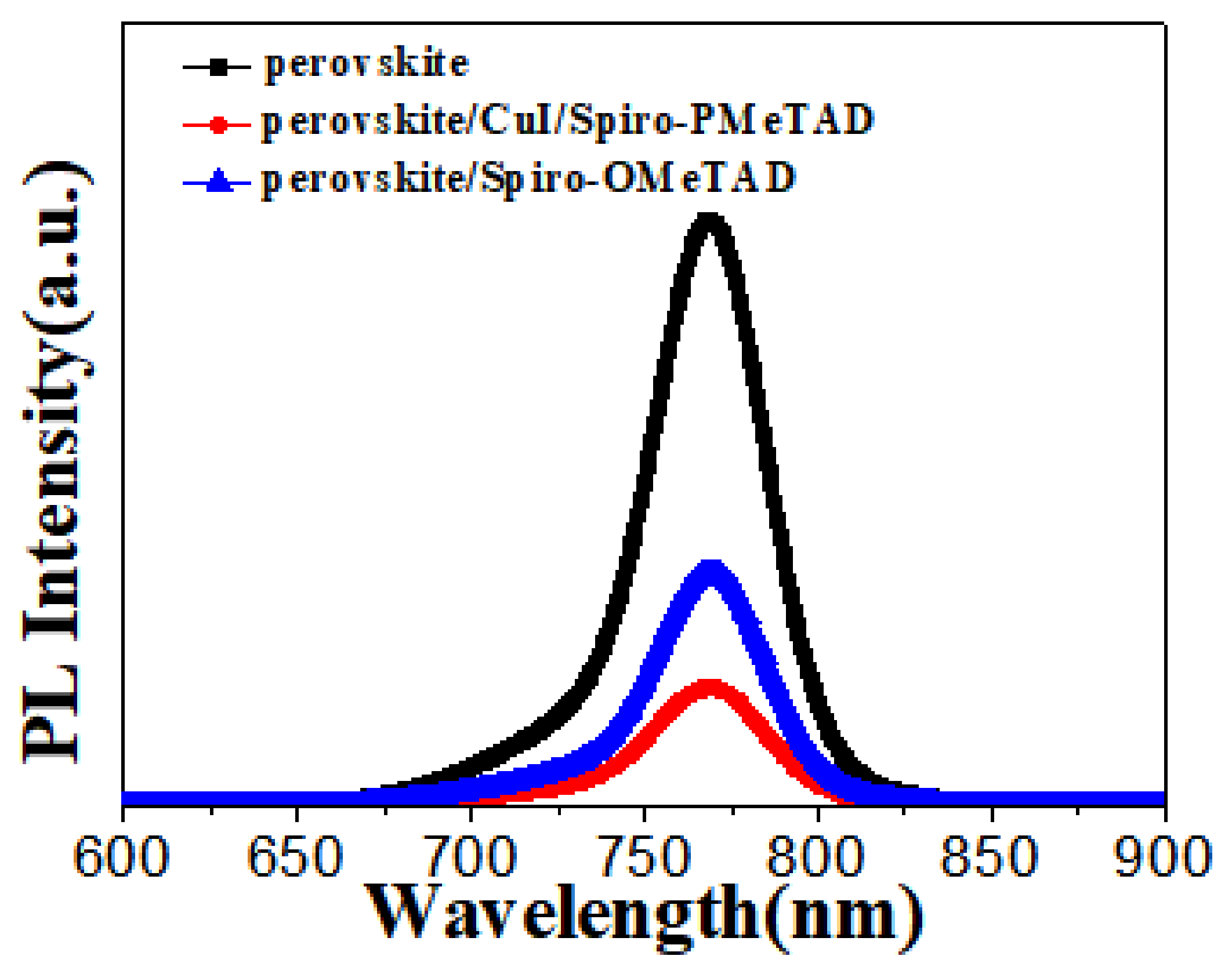
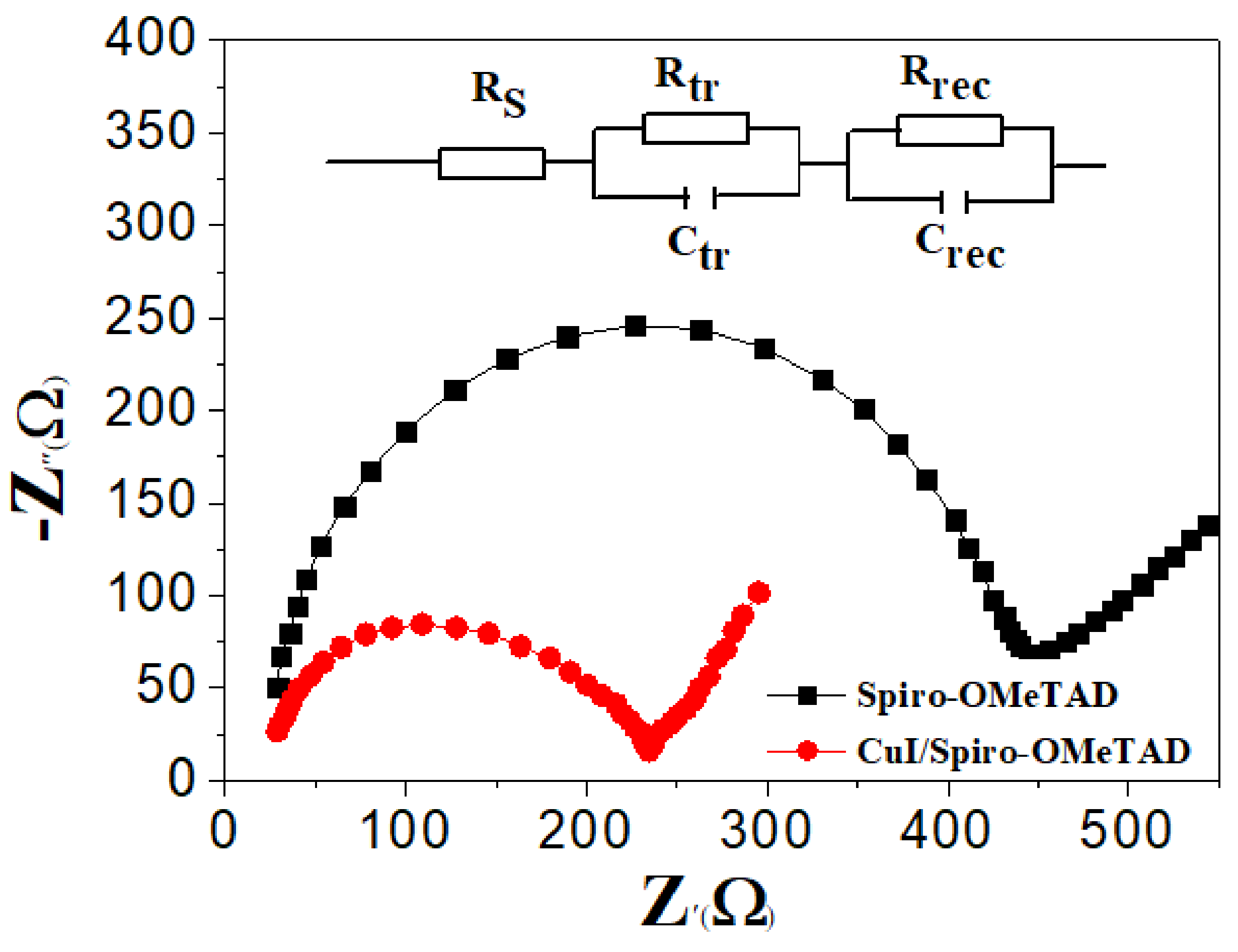
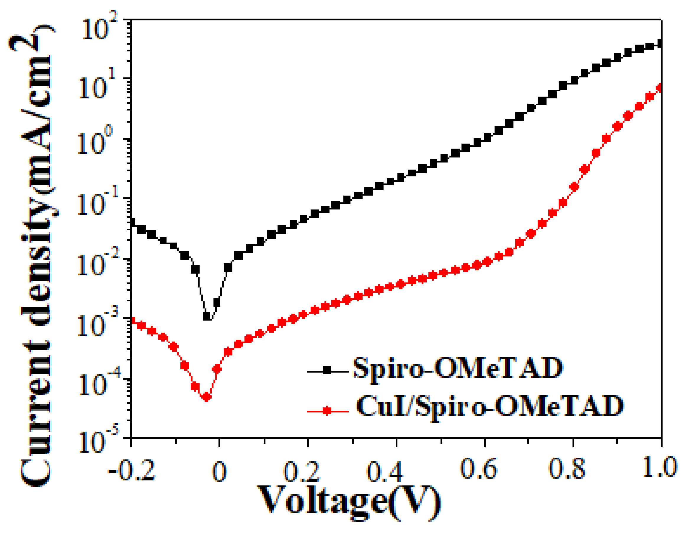
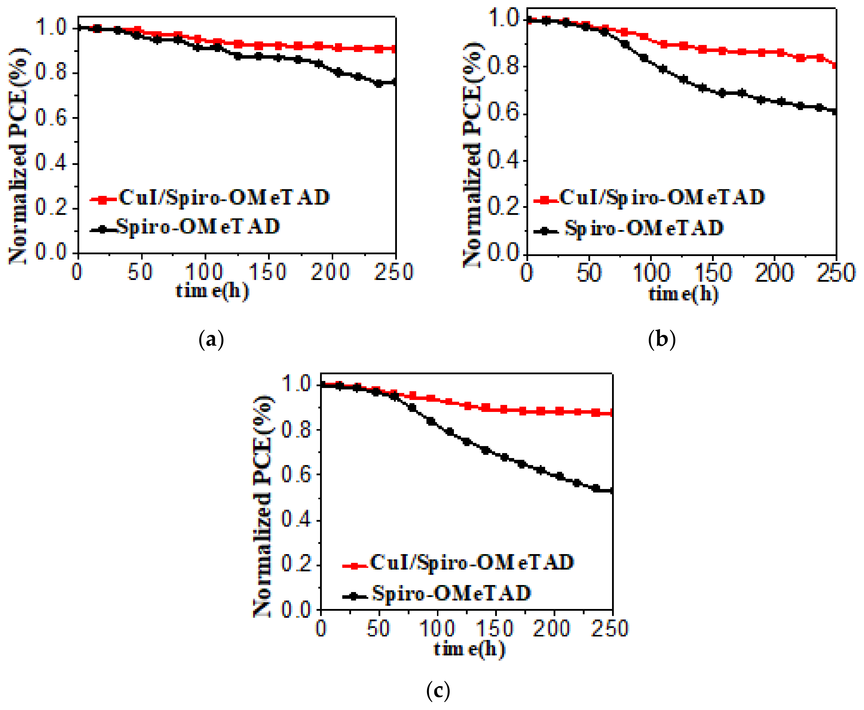
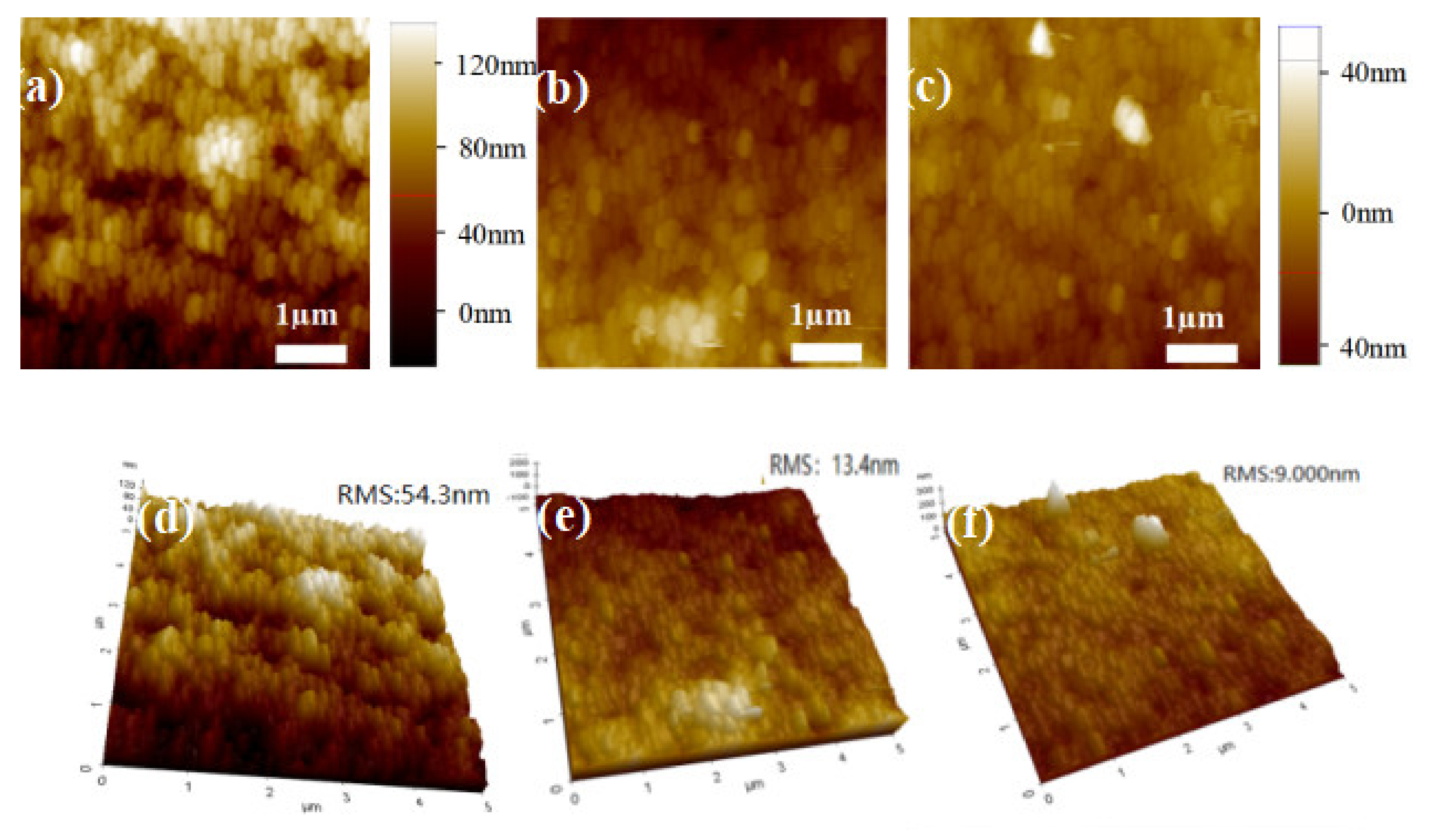
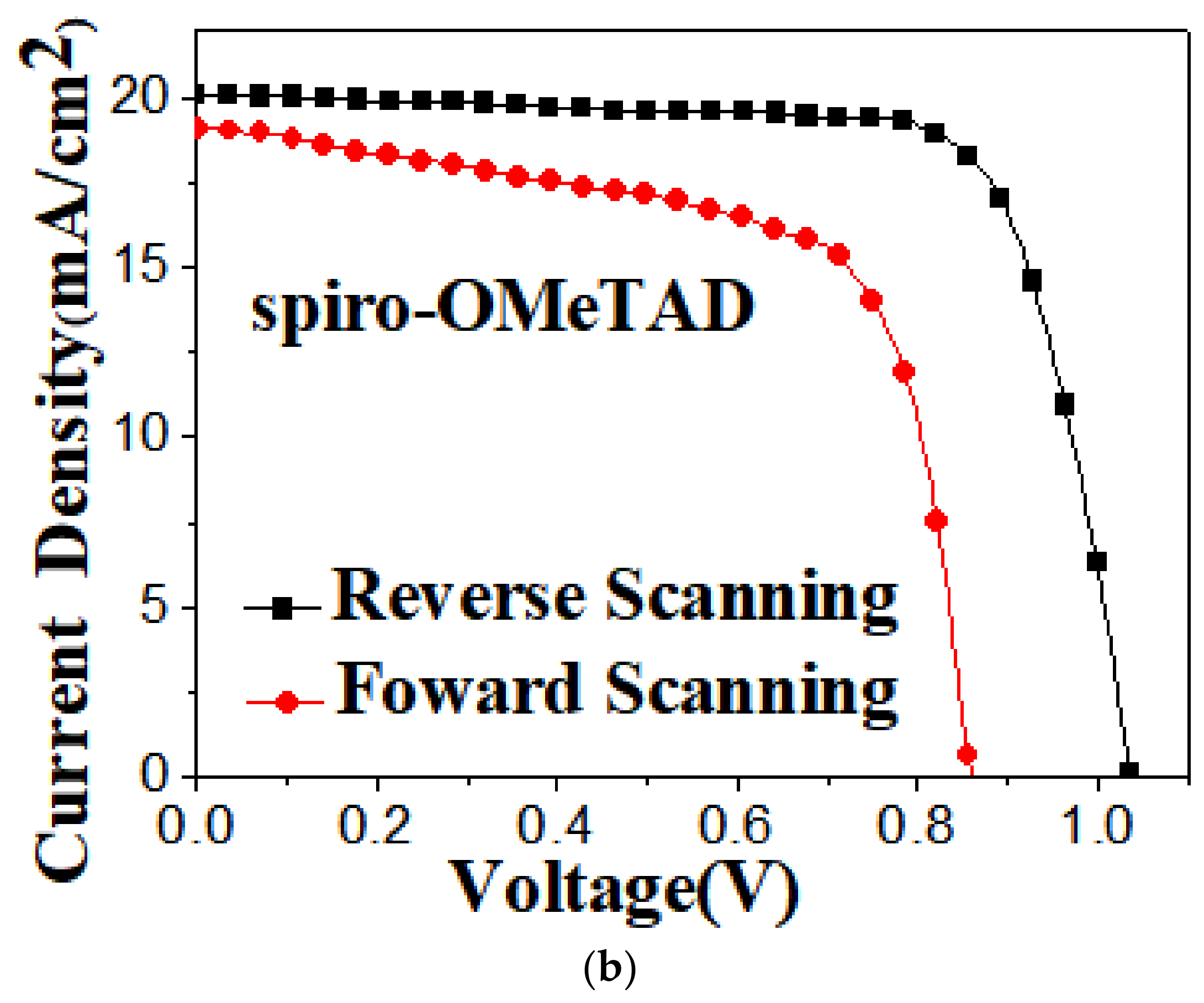
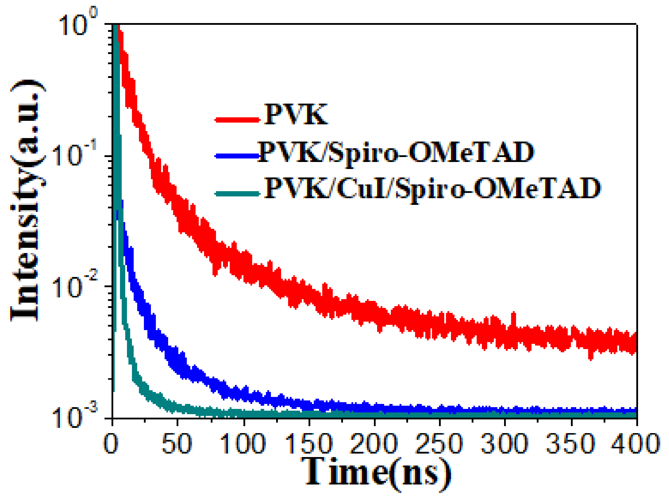
3. Results and Discussion

We referred to the NIP structure planar PSCs (Figure 1a) based on Cs0.05(FA0.87MA0.13)0.95 PbI2.55 Br0.45 as the photoactive layer, wherein Spiro-OMeTAD and SnO2 were spun as the HTL) and ETL [30]. The CuI film was deposited on perovskite by spin coating, and then annealed. Then we spun Spiro-OMeTAD solution and oxidized it naturally in dry air. The cross-section of the perovskite sample can be seen in Figure 1a, which corresponds to the structural diagram of the device. From the figure, we observed that there were obvious boundaries between the different layers. Figure 1b shows the location of the conduction band and the valence band of each layer of the device. For example, the HOMOs of CuI and Spiro-OMeTAD are 5.2 and 5.11 eV, respectively [31], and the Cs0.05(FA0.87MA0.13)0.95 PbI2.55 Br0.45 is 5.44 eV [32]. The insertion of the CuI buffer layer effectively reduced the energy level mismatching between the transport layer and absorption layer. This method effectively reduced the loss of voltage [33].
AFM was applied to compare the surface morphology of the Spiro-OMeTAD and CuI/Spiro-OMeTAD bilayers (Figure 2a–f) on perovskite films, respectively. Perovskite films were spun on SnO2 to form a rough film (Figure 2a,d), and CuI was spun on the perovskite layer (Figure 2b,e). Evaporation and chemical methods were not adopted to obtain CuI layers. We did not adopt evaporation and chemical methods to obtain the CuI layer, mainly due to the fact that spin coating will result in a smooth and dense film [29]. We manufactured several devices to compare how the CuI film optimized the Spiro-OMeTAD-based devices, SnO2/perovskite, SnO2/perovskite/Spiro-OMeTAD and SnO2/perovskite/CuI/Spiro-OMeTAD. Figure 1c,f represent the fact that the CuI film is conducive to the Spiro-OMeTAD growing film, and CuI film can fill the pinholes on Spiro-OMeTAD films.
According to the research of Park et al., the Spiro-OMeTAD layer contains numerous of pinholes which lead to a high leakage current and serious electron-hole recombination [14]. The inserted buffer layer CuI can prevent the acetonitrile in Spiro-OMeTAD from corroding the perovskite film, and the pinholes in the Spiro-OMeTAD film are filled. At the same time, the passivation layer can reduce the boundary trap density.
XRD patterns on different substrates of CuI were measured as seen in Figure 3. By testing the XRD of FTO conductive substrate and FTO conductive substrate covering CuI film, and then subtracting the two XRD images, the obtained XRD image is CuI’s XRD on the FTO conductive substrate. Similarly, the XRD of CuI on perovskite surface can be obtained. XRD results show that CuI is located on the surface of FTO and FTO/perovskite, respectively. From the XRD pattern of CuI, it can be seen that the (111) peak phase of the annealed CuI crystal based on FTO and FTO/perovskite surface is the same, indicating that the crystal obtained after annealing before and after spin coating on perovskite surface is the desired structure, and has not been oxidized or decomposed. The only difference is that the (111) peak on the surface of FTO/perovskite is sharper, which indicates that the CuI crystal on the surface of perovskite has a better crystal phase.
Figure 4 shows the XPS of CuI measured on the surface of perovskite crystal to prove a peak spectrum of Cu 2p of Cu+ in CuI. The figure shows the FTO/CuI spectrum. That is to say, after dissolving CuI powder, it was spin coated on the surface of perovskite and then annealed and crystallized to obtain non-oxidized Cu+. This is consistent with the (111) phase of CuI crystal measured by XRD. CuI composition did not change before and after treatment. Tzung Fang Guo et al. improved the photoelectric characteristics of perovskite photovoltaic devices by doping CuI in the perovskite absorption layer. CuI does not exchange molecules with perovskite, but only distributes in the perovskite grain boundary to passivate defects [34]. The crystal plays a positive role in hole transport and electron blocking of perovskite photovoltaic devices.
The compact CuI layer is not only used for transmission, but also used to protect the absorption layer to improve the efficiency of the solar cells. The photocurrent voltage (J-V) curves of champion devices were prepared in N2 gloveboxes with different thicknesses of CuI, which are compared in Figure 5. The VOC, JSC (short-circuit current), FF and PCE are measured according to the statistical data of 50 independent devices. The results are summarized in Table 1. The different spin coating speed of CuI of organic–inorganic double-layer CuI/Spiro-OMeTAD exhibited an effect on the device efficiency. Based on the single Spiro-OMeTAD HTLs material, the champion device VOC was 1.05 V, JSC was 20.05 mA/cm2, FF was 71.99%, and the best PCE was 15.16%. For the devices based on double HTLs, when the CuI solution was 20 mg/mL and spin coating at 4000 r/min, in the optimal data, the best PCE was 17.44%, JSC was 20.10 mA/cm2, VOC was 1.10 V and FF was 78.88%, as shown in Figure 5a. Therefore, we used a CuI solution at 4000 r/min spin speed deposited the HTL additive layer. In the following section, we compare the performance of the double-layer hole transport solar cells with that of the single-layer solar cells, based on the device with a spin speed of 4000 r/min.
The EQE spectra in Figure 5b were obtained for several PSC devices. The JSC value obtained from the EQE spectral integration was a little smaller than the value obtained from the J-V curve as shown in Figure 5a, and the two values could match well. If the JSC values are different in EQE and the J-V curves do not match well, it can prove that the light response of the solar cells is not very good; the hysteresis is obvious. The enhancement of champion device performance was further confirmed with the EQE spectrum. The integrated JSC calculated from the EQE spectrum of the champion device was 20.00 mA/cm2, which is in good agreement with the measured(mA/cm2). More interestingly, the champion cell exhibited a panchromatic plateau of higher average value in the highest part of the 250–800 nm range.
As shown in Figure 6a–d, there were VOC, JSC, FF, PCE box plots based on 20 initially unoptimized and CuI optimized perovskite photovoltaic devices, respectively. It was clearly found that the highest PCE of the optimized perovskite photovoltaic cells was 17.44% and the average PCE was 17.30%, which was much higher than the PCE of the perovskite photovoltaic devices not modified by CuI in any aspect. After analysis, it was further found that the higher PCE was due to the improvement of FF and JSC. The optimized perovskite photovoltaic devices were higher than that of the initial perovskite photovoltaic devices, and the optimized FF and PCE values were more concentrated, while the initial device values were more divergent, which further illustrates the repeatability of optimized perovskite photovoltaic devices.
For further study of the solar cells, we prepared the complete solar cells with Spiro-OMeTAD and CuI/Spiro-OMeTAD. From Figure 7, the reverse and forward scanning results, it can be observed that the hysteresis of the single HTL samples was quite serious, while that of the CuI/Spiro-OMeTAD double samples was negligible. Next, we used the hysteresis index [35,36] defined by Equation (1) to quantify the hysteresis change in the photocurrent-voltage (J-V) curve:
HI = J R V O C 2 J F V O C 2 J R V O C 2
where JR (Voc/2) is related to the photocurrent and VOC during reverse scanning, and JF (Voc/2) is the photocurrent during forward scanning. It is generally believed that the smaller the HI is, the smaller the hysteresis of the solar devices will be. The HI is typically between 0 and 1. Here the calculated HI values are 0.17 and 0.005 for devices with single and double HTLs, respectively. As a result of the pinholes between the HTL and perovskite, the perovskite makes contact with the electrode or air directly, resulting in defects. The insertion of CuI avoids the direct contact between Spiro-OMeTAD and perovskite, thereby reducing the number of interface defects, and this is conducive to the collection and transportation of charges, thus reducing recombination. The solar cells hysteresis after optimization is negligible. Therefore, the double HTLs can reduce the hysteresis significantly.
The electron trap-state density between the perovskite layer and HTLs was measured with the aid of a space charge limited current (SCLC) (Figure 8). A regular solar cell of ITO/NiO/perovskite/HTL/Au was prepared, and the corresponding dark J-V curves are shown in Figure 6a,b, for which the trap-state densities were calculated to be 1.4 × 1016 cm−3 and 1.7 × 1016 cm−3 for CuI/Spiro-OMeTAD and Spiro-OMeTAD HTLs, respectively. Such a decrease in the N defect value by around 20% for the CuI/Spiro-OMeTAD cells showed that the defects concentration between the absorption layer and transport layer reduced to a large extent. A persuasive statement for the reduced defect is that the CuI thin layer deposit on the rough perovskite layer filled the small pinholes on the Spiro-OMeTAD HTL, resulting in a more uniform and smoother layer; this was due to the CuI layer leading to the Spiro-OMeTAD layer having intimate contact with the Au electrodes [14]. On the other hand, the addition of CuI film was conducive to hole charge extraction.
Next, the charge carrier recombination dynamics of the two different devices were studied by light intensity dependent VOC. As shown in Figure 9, when the light intensity changes, linear correlation can be obtained. The slopes of the lines for the pristine and double HTLs solar cells near one, thus demonstrate that the charges recombination of the two devices at low light intensity can be ignored [37,38]. The most important recombination is the defect recombination between the perovskite and transport layers [39]. The ideal factors reflect the trap recombination, which describes the relationship between light intensity and voltage, as shown in Figure 9. The N changed from 1.45 of the pristine Spiro-OMeTAD-based solar cells to 1.38 of the CuI/Spiro-OMeTAD-based devices, thereby indicating that the decrease in interface defect density inhibited the trap recombination process. First, the well-matched energy level arrangement at the perovskite/CuI/Spiro-OMeTAD/Au electrode interface enhanced the ability to extract photogenerated holes from perovskite films and inject the holes into the Au electrodes. Second, the CuI intermediate layer prevented the Au electrode particles entering the absorption layer, formed an ideal energy barrier, prevented the flow of electrons to Au electrode, and greatly inhibited the recombination of the perovskite/Spiro-OMeTAD/Au interface. Third, the CuI layer could passivate the surface defect state of perovskite, thereby greatly reducing the recombination of photocarriers in the devices.
The steady state photoluminescence (PL) spectra (Figure 10) shows the strong PL emission of perovskite films at 763 nm [40]. Perovskite film on glass substrate has the highest photoluminescence intensity, which indicates that there is serious carrier re-combination in the sample. Clearly, the photoquenching efficiency of perovskite/CuI/Spiro-OMeTAD is greater than that of perovskite/Spiro-OMeTAD, showing effective charge extraction.
The charge recombination lifetime of perovskite solar cells was evaluated by time-resolved photoluminescence (TRPL) (Figure 11) for the structure of single perovskite, perovskite/Spiro-OMeTAD, and perovskite/CuI/Spiro-OMeTAD. The TRPL are fitted by the bi-exponential function:
f ( t ) = A e t / τ 1 + B e t / τ 2 + C
In the equation, the fast transient component τ 1 corresponds to the surface characteristics and the slow component τ 2 corresponds to the volume characteristics. A and B represent the contribution of speed. C is a constant [41]. The average decay lifetime is obtained through the following function:
τ a v e = A ι τ ι 2 A ι τ ι
Based on single HTL and double HTLs perovskite solar cells, the average photoluminescence lifetime ( τ a v e ) of the extracted perovskite samples (70.4 ns) is greatly reduced to 51.22 and 44.48 ns, respectively (Figure 11).
Compared with single HTL, the PL lifetime of double HTLs samples is much shorter, which signifies that the hole transfer process has been improved. This suggests that light-generated carriers can be effectively transferred to HTL. These results indicate that there is an effective hole transfer and reduction in recombination centers between the perovskite and double hole transport layers, which is necessary for effective charge extraction and collection in perovskite devices.
The EIS was applied studying the carrier transport at the interface. Figure 12 shows the Nyquist plots based on the Spiro-OMeTAD and double CuI/Spiro-OMeTAD HTLs layers. The high frequency arc is due to the transport characteristics of carriers in the bulk layer. The low frequency incomplete semicircle represents the carrier recombination process of carriers at the interface. The values of Rtr and Rrec were fitted by Z-view software. Compared with the single HTL Spiro-OMeTAD device, the double CuI/Spiro-OMeTAD HTLs device had a smaller Rtr and larger Rrec. As it had the same preparation conditions except for different HTMs, the shape of the EIS curve depends on the result of HTM and the interface it modified. Additionally, because of the arrangement of energy levels, the CuI layer can prevent the hole diffusion from the Spiro-OMeTAD, which indicates that the interface electron-hole recombination between the ETL and HTL has been reduced. Moreover, a uniform and smoother layer of Spiro-OMeTAD was obtained, which is derived from the fact that the CuI scaffold layer was in close contact with the counter electrode. The results show that the charge carrier transfer rate of double HTLs devices was faster, and the recombination rate was lower, which is consistent with the TRPL results.
According to the equation of V o c = n k T q ln J S C J O + 1 [42], the VOC is related to photocurrent JSC and dark current JO, and the VOC decreases as the JO increases from the equation. However, the dark current is determined by defects in the perovskite and the interface of the perovskite solar cells. Therefore, the dark state current can be used as a standard by which to evaluate the perovskite solar cells’ performance. In order to obtain a better perovskite solar cell VOC, a lower dark current is necessary.
Dark state J-V curves were used to evaluate the quality of the solar cells, which is shown in Figure 13. The current was suppressed with double HTLs. CuI compensated for the defect of Spiro-OMeTAD on the perovskite layer, and impeded the contact between air and perovskite, thereby effectively reducing the defects of the interface and the solar cell, in turn resulting in a reduction in dark current compared to devices of single HTL devices. These results are highly consistent with the EIS measurements.
After a variety of optimization measures, the most important measurement standard of perovskite photovoltaic devices is to improve the stability on the basis of improving the efficiency, so as to facilitate the practicability of the research results. In this paper, the stability of double hole transport layer perovskite photovoltaic cells optimized by CuI was tested after encapsulation. Under the encapsulation conditions, the perovskite photovoltaic devices can avoid the influence of humidity, mainly due to the influence of temperature and light. Due to the defects and holes in the interface between perovskite and Spiro, the charge recombination and the decomposition of perovskite led to a decrease in the efficiency of perovskite photovoltaic devices, the stability of encapsulation photovoltaic devices (non-optimized and optimized), devices under normal light and temperature, the stability of packaged photovoltaic devices, (non-optimized and optimized), devices under ultraviolet light and normal temperature, and the stability of packaged photovoltaic devices (non-optimized and optimized devices) under normal light and 80 °C.
As shown in Figure 14a, the stability of the encapsulation perovskite photovoltaic devices (non-optimized and optimized devices) under am 1.5g illumination (RH ≤ 30%) in ambient conditions was measured. It can be seen from the figure that under the conditions of laboratory tests and normal illumination, after continuous illumination for 250 h, the photoelectric efficiency of the perovskite photovoltaic device based on CuI/Spiro-OMeTAD double-layer hole transport layer structure became 90% of the beginning structure, while the efficiency of the perovskite photovoltaic device based on single-layer Spiro-OMeTAD hole transport layer decreased to 75% of the beginning photoelectric efficiency. This is due to the defects in the interface between perovskite and Spiro-OMetad, and the slight decomposition of perovskite under continuous illumination, which leads to the degradation of perovskite properties.
As shown in Figure 14b, under laboratory conditions, the temperature was kept at room temperature, and the light was changed to ultraviolet light. The stability of the encapsulation perovskite photovoltaic device (non-optimized and optimized devices) was improved. It can be found that under the influence of ultraviolet light, after 250 h of continuous irradiation, the efficiency of the photovoltaic device based on CuI/Spiro-OMeTAD double-layer hole transport layer was 80% of the original efficiency, while the efficiency of the perovskite photovoltaic solar cell based on single-layer Spiro-OMeTAD hole transport layer was 60%. This is due to the accelerated decomposition of the perovskite absorption layer under UV irradiation, and the defects in the perovskite crystal and Spiro-OMeTAD interface also led to the decomposition of perovskite photovoltaic devices. This led to a decrease in the efficiency of photovoltaic devices.
As shown in Figure 14c, under am 1.5 g illumination (RH ≤ 30%) in ambient conditions and at 80 °C, the stability of the encapsulation perovskite photovoltaic devices non-optimized and optimized devices was compared. Under certain conditions, after 250 h of continuous irradiation, the efficiency of the photovoltaic device based on CuI/Spiro-OMeTAD double-layer hole transport layer was 85% of the original efficiency, while the efficiency of the perovskite photovoltaic solar cells based on single-layer Spiro-OMeTAD hole transport layer was 55%. At a high temperature, the perovskite absorption layer will also accelerate the decomposition of the absorption layer components and become a toxic material which is not conducive to perovskite photoelectric conversion. Thus, the performance of perovskite photovoltaic devices is reduced.

4. Conclusions

In this study, we adopted a perovskite solar cell device with an upright structure. We inserted a CuI layer between perovskite and Spiro-OMeTAD by means of the one-step method prepared in N2 gloveboxes. The CuI layer deposited on the perovskite surface was annealed by solution spin coating, because liquid spin coating is a low-cost and easy to control means. The CuI layer and Spiro -OMeTAD layer produced by spin coating formed a double-layer hole transport layer. The CuI on perovskite layer reduced the perovskite roughness, and also reduced the Spiro-OMeTAD roughness, resulting in a better connection between the Au electrode and Spiro-OMeTAD. In addition, CuI reducing defect density is conducive to hole extraction, and improves the collection of hole carriers at the Au electrode. For these reasons, the CuI/Spiro-OMeTAD double HTLs devices achieved an improved PCE of 17.44%. More importantly, without encapsulation, a PCE degradation of only 10% was shown in the aging test for 250 h. Meanwhile, the hysteresis of perovskite solar cells modified by double cavity transport layer can be ignored. The double HTLs model offers an easy means by which to realize high-quality and stable perovskite films for optoelectronic applications. Our work demonstrates that double HTLs can be the promising HTLs for high performance and environmentally stable PSCs.

Author Contributions

C.L.: conceptualization, methodology, investigation, formal analysis, writing—Original Draft, Writing—review and editing. Z.J.: investigation, methodology, formal analysis. Y.Z.: investigation, methodology, formal analysis, resources. C.N.: investigation, formal analysis. W.Z.: methodology, resources, formal analysis, writing—review and editing, supervision, project administration, funding acquisition. All authors have read and agreed to the published version of the manuscript.

Funding

The authors gratefully acknowledge Beihang University for providing access to experimental equipment to be used for sample fabrication and measurement. The project as a whole is supported by the National Natural Science Foundation of China (grant no. 51572008).

Institutional Review Board Statement

Not applicable.

Informed Consent Statement

Not applicable.

Data Availability Statement

The data in this work are available on request from the corresponding author.

Acknowledgments

The authors would like to acknowledge Beijing University of Aeronautics and Astronautics technical and financial support to this research.

Conflicts of Interest

The authors declare no conflict of interest.

References

  1. Xu, Z.; Jiang, Y.; Li, Z.; Chen, C.; Kong, X.; Chen, Y.; Zhou, G.; Liu, J.; Kempa, K.; Gao, J. Rapid microwave-assisted synthesis of SnO2 quantum dots for efficient planar perovskite solar cells. ACS Appl. Energy Mater. 2021, 4, 1887–1893. [Google Scholar] [CrossRef]
  2. Tong, J.; Gong, J.; Hu, M.; Yadavalli, S.K.; Dai, Z.; Zhang, F.; Xiao, C.; Hao, J.; Yang, M.; Anderson, M.A.; et al. High-performance methylammonium-free ideal-band-gap perovskite solar cells. Matter 2021, 4, 1–12. [Google Scholar] [CrossRef]
  3. Yusoff, A.R.B.M.; Vasilopoulou, M.; Georgiadou, D.G.; Palilis, L.C.; Abate, A.; Nazeeruddin, M.K. Passivation and process engineering approaches of halide perovskite films for high efficiency and stability perovskite solar cells. Energy Environ. Sci. 2021, 14, 2906–2953. [Google Scholar] [CrossRef]
  4. Kim, S.; Kim, G.; Moon, C.S.; Yang, T.; Seo, J. Metal-free phthalocyanine as a hole transporting material and a surface passivator for efficient and stable perovskite solar cells. Small Methods 2021, 5, 2001248. [Google Scholar] [CrossRef]
  5. Gao, Z.W.; Wang, Y.; Liu, H.; Sun, J.; Kim, J.; Li, Y.; Xu, B.; Choy, W.C.H. Tailoring the interface in FAPbI3 planar perovskite solar cells by Imidazole-Graphene-Quantum-Dots. Adv. Funct. Mater. 2021, 31, 2101438. [Google Scholar] [CrossRef]
  6. Zhuang, J.; Mao, P.; Luan, Y.; Chen, N.; Cao, X.; Niu, G.; Jia, F.; Wang, F.; Cao, S.; Wang, J. Rubidium fluoride modified SnO2 for planar n-i-p perovskite solar cells. Adv. Funct. Mater. 2021, 31, 2010385. [Google Scholar] [CrossRef]
  7. Kojima, A.; Teshima, K.; Shirai, Y.; Miyasaka, T. Organometal Halide Perovskites as Visible-Light Sensitizers for Photovoltaic Cells. J. Am. Chem. Soc. 2009, 131, 6050–6056. [Google Scholar] [CrossRef]
  8. NREL. Best Research-Cell Efficiency Chart. 2020. Available online: https://www.nrel.gov/pv/cellefficiency.html (accessed on 18 May 2021).
  9. Yu, Z.; Sun, L. Recent Progress on Hole-Transporting Materials for Emerging Organometal Halide Perovskite Solar Cells. Adv. Energy Mater. 2015, 5, 1500213. [Google Scholar] [CrossRef]
  10. Park, J.H.; Seo, J.; Park, S.; Shin, S.S.; Kim, Y.C.; Jeon, N.J.; Shin, H.-W.; Ahn, T.K.; Noh, J.H.; Yoon, S.C.; et al. Efficient CH3NH3PbI3 perovskite solar cells employing nanostructured p-type NiO electrode formed by a pulsed laser deposition. Adv. Mater. 2015, 27, 4013–4019. [Google Scholar] [CrossRef]
  11. Jung, E.H.; Jeon, N.J.; Park, E.Y.; Moon, C.S.; Shin, T.J.; Yang, T.Y.; Noh, J.H.; Seo, J. Efficient, stable and scalable perovskite solar cells using poly(3-hexylthiophene). Nature 2019, 567, 511–515. [Google Scholar] [CrossRef]
  12. Xi, H.; Tang, S.; Ma, X.; Chang, J.; Chen, D.; Lin, Z.; Zhong, P.; Wang, H.; Zhang, C. Performance Enhancement of Planar Heterojunction Perovskite Solar Cells through Tuning the Doping Properties of Hole-Transporting Materials. ACS Omega 2017, 2, 326–336. [Google Scholar] [CrossRef] [Green Version]
  13. Kim, Y.; Jung, E.H.; Kim, G.; Kim, D.; Kim, B.J.; Seo, J. Sequentially Fluorinated PTAA Polymers for Enhancing VOC of High-Performance Perovskite Solar Cells. Adv. Energy Mater. 2018, 8, 1801668. [Google Scholar] [CrossRef]
  14. Kim, G.; Kang, G.; Choi, K.; Choi, H.; Park, T. Solution Processable Inorganic–Organic Double-Layered Hole Transport Layer for Highly Stable Planar Perovskite Solar Cells. Adv. Energy Mater 2018, 8, 1801386. [Google Scholar] [CrossRef]
  15. Dunlap-Shohl, W.A.; Daunis, T.B.; Wang, X.; Wang, J.; Zhang, B.; Barrera, D.; Yan, Y.; Hsu, J.W.; Mitzi, D.B. Room-temperature fabrication of a delafossite CuCrO2 hole transport layer for perovskite solar cells. J. Mater. Chem. A 2018, 6, 469–477. [Google Scholar] [CrossRef]
  16. Chen, W.; Zhou, Y.; Chen, G.; Wu, Y.; Tu, B.; Liu, F.Z.; Huang, L.; Ng, A.M.C.; Djurišić, A.B.; He, Z. Alkali Chlorides for the Suppression of the Interfacial Recombination in Inverted Planar Perovskite Solar Cells. Adv. Energy Mater. 2019, 9, 1803872. [Google Scholar] [CrossRef]
  17. Chen, Y.; Yang, Z.; Jia, X.; Wu, Y.; Yuan, N.; Ding, J.; Zhang, W.-H.; Liu, S. Thermally stable methylammonium-free inverted perovskite solar cells with Zn2+ doped CuGaO2 as efficient mesoporous hole-transporting layer. Nano Energy 2019, 61, 148–157. [Google Scholar] [CrossRef]
  18. Papadas, I.T.; Savva, A.; Ioakeimidis, A.; Eleftheriou, P.; Armatas, G.S.; Choulis, S.A. Employing surfactant-assisted hydrothermal synthesis to control CuGaO2 nanoparticle formation and improved carrier selectivity of perovskite solar cells. Mater. Today Energy 2018, 8, 57–64. [Google Scholar] [CrossRef] [Green Version]
  19. Mali, S.S.; Patil, J.V.; Kim, H.; Luque, R.; Hong, C.K. Highly efficient thermally stable perovskite solar cells via Cs:NiO/CuSCN double-inorganic hole extraction layer interface engineering. Mater. Today 2019, 26, 8–18. [Google Scholar] [CrossRef]
  20. Jiang, F.; Choy, W.C.; Zhang, X.; Li, D.; Cheng, J. Post-treatment-Free Solution-Processed Non-stoichiometric NiOx Nanoparticles for Efficient Hole-Transport Layers of Organic Optoelectronic Devices. Adv. Mater. 2015, 27, 2930–2937. [Google Scholar] [CrossRef]
  21. Du, Y.; Xin, C.; Huang, W.; Shi, B.; Ding, Y.; Wei, C.; Zhao, Y.; Li, Y.; Zhang, X. Polymeric Surface Modification of NiOx-Based Inverted Planar Perovskite Solar Cells with Enhanced Performance. ACS Sustain. Chem. Eng. 2018, 6, 16806–16812. [Google Scholar] [CrossRef]
  22. Tang, L.J.; Chen, X.; Wen, T.Y.; Yang, S.; Zhao, J.J.; Qiao, H.W.; Hou, Y.; Yang, H.G. A Solution-Processed Transparent NiO Hole-Extraction Layer for High-Performance Inverted Perovskite Solar Cells. Chemistry 2018, 24, 2845–2849. [Google Scholar] [CrossRef]
  23. Yin, X.; Zhai, J.; Wang, T.; Jing, W.; Song, L.; Xiong, J. Mesoporous NiO nanosheet network as efficient hole transporting layer for stable inverted perovskite solar cells. Mater. Lett. 2018, 231, 101–104. [Google Scholar] [CrossRef]
  24. Nazari, P.; Ansari, F.; Nejand, B.A.; Ahmadi, V.; Payandeh, M.; Niasari, M.S. Physicochemical Interface Engineering of CuI/Cu as Advanced Potential Hole-Transporting Materials/Metal Contact Couples in Hysteresis-Free Ultralow-Cost and Large-Area Perovskite Solar Cells. J. Phys. Chem. C 2017, 121, 21935–21944. [Google Scholar] [CrossRef]
  25. Yin, X.; Chen, P.; Que, M.; Xing, Y.; Que, W.; Niu, C.; Shao, J. Highly Efficient Flexible Perovskite Solar Cells Using Solution-Derived NiOx Hole Contacts. ACS Nano 2016, 10, 3630–3636. [Google Scholar] [CrossRef]
  26. Zhang, H.; Wang, H.; Zhu, H.; Chueh, C.; Chen, W.; Yang, S.; Jen, A. Low-Ttemperatue Solution-Processed CuCrO2 Hole-Transporting Layer for Efficient and Photostable Perovskite Solar Cells. Adv. Energy Mater. 2018, 8, 1702762. [Google Scholar] [CrossRef]
  27. Byranvand, M.M.; Kim, T.; Song, S.; Kang, G.; Ryu, S.U.; Park, T. p-Type CuI Islands on TiO2 Electron Transport Layer for a Highly Efficient Planar-Perovskite Solar Cell with Negligible Hysteresis. Adv. Energy Mater. 2018, 8, 1702235. [Google Scholar] [CrossRef]
  28. Wang, H.; Yu, Z.; Lai, J.; Song, X.; Yang, X.; Hagfeldt, A.; Sun, L. One plus one greater than two: High-performance inverted planar perovskite solar cells based on a composite CuI/CuSCN hole-transporting layer. J. Mater. Chem. A 2018, 6, 21435–21444. [Google Scholar] [CrossRef]
  29. Sun, W.; Ye, S.; Rao, H.; Li, Y.; Liu, Z.; Xiao, L.; Chen, Z.; Bian, Z.; Huang, C. Room-temperature and solution-processed copper iodide as the hole transport layer for inverted planar perovskite solar cells. Nanoscal 2016, 8, 15954–15960. [Google Scholar] [CrossRef]
  30. Wei, J.; Guo, F.; Wang, X.; Xu, K.; Lei, M.; Liang, Y.; Zhao, Y.; Xu, D. Sno2-in-Polymer Matrix for High-Efficiency Perovskite Solar Cells with Improved Reproducibility and Stability. Adv. Mater. 2018, 30, 1805153. [Google Scholar] [CrossRef] [PubMed]
  31. Casas, G.A.; Cappelletti, M.A.; Cédola, A.P.; Soucase, B.M.; Blancá, E.L. Analysis of the power conversion efficiency of perovskite solar cells with different materials as Hole-Transport Layer by numerical simulations. Superlattices Microstruct. 2017, 107, 136e143. [Google Scholar] [CrossRef]
  32. Wolff, C.M.; Zu, F.; Paulke, A.; Toro, L.P.; Koch, N.; Neher, D. Reduced Interface-Mediated Recombination for High Open-Circuit Voltages in CH3NH3PbI3 Solar Cells. Adv. Mater. 2017, 29, 1700159. [Google Scholar] [CrossRef] [PubMed]
  33. Wang, G.; Dong, W.; Gurung, A.; Chen, K.; Wu, F.; He, Q.; Pathak, R.; Qiao, Q. Improving photovoltaic performance of carbon-based CsPbBr3 perovskite solar cells by interfacial engineering using P3HT interlayer. J. Power Sources 2019, 432, 48–54. [Google Scholar] [CrossRef]
  34. Wu, P.; Hu, C.; Chen, L.; Lin, P.; Guo, T.; Fu, Y. Cuprous iodide dose dependent passivation of MAPbI3 perovskite solar cells. Org. Electron. 2021, 19, 106080. [Google Scholar] [CrossRef]
  35. Sanchez, R.S.; Gonzalez-Pedro, V.; Lee, J.-W.; Park, N.-G.; Kang, Y.S.; Mora-Sero, I.; Bisquert, J. Slow Dynamic Processes in Lead Halide Perovskite Solar Cells. Characteristic Times and Hysteresis. J. Phys. Chem. Lett. 2014, 5, 2357–2363. [Google Scholar] [CrossRef]
  36. Yu, H.; Lu, H.; Xie, F.; Zhou, S.; Zhao, N. Native defect-induced hysteresis behavior in organolead iodide perovskite solar cells. Adv. Funct. Mater. 2016, 26, 1411–1419. [Google Scholar] [CrossRef]
  37. Cowan, S.R.; Street, R.A.; Cho, S.; Heeger, A.J. Transient photoconductivity in polymer bulk heterojunction solar cells: Competition between sweep-out and recombination. Phys. Rev. B 2011, 83, 035205. [Google Scholar] [CrossRef]
  38. Davies, C.L.; Filip, M.R.; Patel, J.B.; Crothers, T.W.; Verdi, C.; Wright, A.D.; Milot, R.L.; Giustino, F.; Johnston, M.B.; Herz, L.M. Bimolecular recombination in methylammonium lead triiodide perovskite is an inverse absorption process. Nat. Commun. 2018, 9, 293. [Google Scholar] [CrossRef] [Green Version]
  39. Johnston, M.B.; Herz, L.M. Hybrid Perovskites for Photovoltaics: Charge-Carrier Recombination, Diffusion, and Radiative Efficiencies. Acc. Chem. Res. 2016, 49, 146–154. [Google Scholar] [CrossRef] [PubMed] [Green Version]
  40. Yang, Y.; Pham, N.D.; Yao, D.; Fan, L.; Hoang, M.T.; Tiong, V.T.; Wang, Z.; Zhu, H.; Wang, H. Interface Engineering to Eliminate Hysteresis of Carbon-Based Planar Heterojunction Perovskite Solar Cells via CuSCN Incorporation. ACS Appl. Mater. Interfaces 2019, 11, 28431–28441. [Google Scholar] [CrossRef]
  41. Lee, J.W.; Kim, H.S.; Park, N.G. Lewis acid–base adduct approach for high efficiency perovskite solar cells. Acc. Chem. Res. 2016, 49, 311–319. [Google Scholar] [CrossRef]
  42. Li, R.; Wang, P.; Chen, B.; Cui, X.; Ding, Y.; Li, Y.; Zhang, D.; Zhao, Y.; Zhang, X. NiOx/Spiro Hole Transport Bilayers for Stable Perovskite Solar Cells with Efficiency Exceeding 21%. ACS Energy Lett. 2020, 5, 79–86. [Google Scholar] [CrossRef]
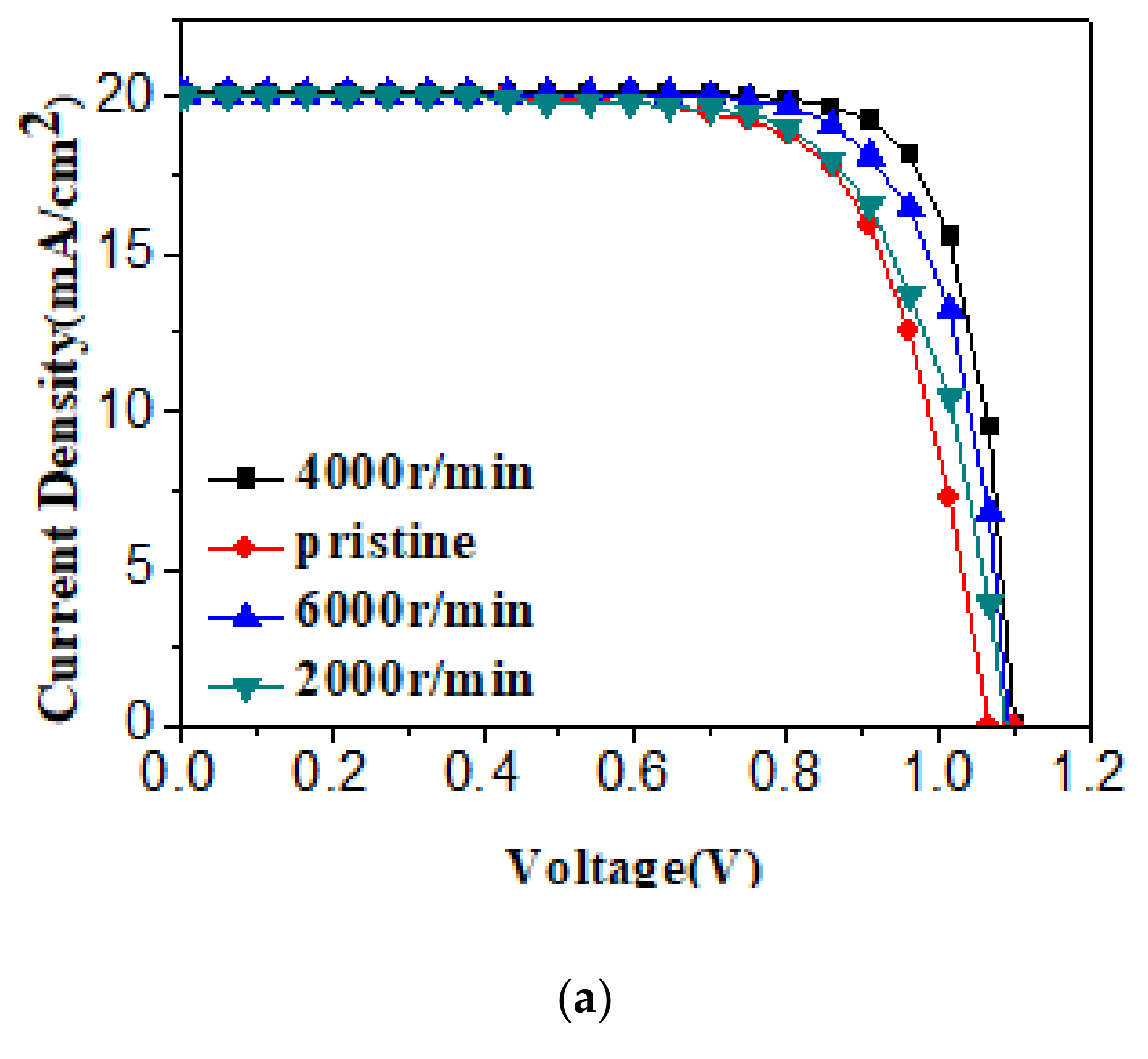
Figure 1. (a) Cross-sectional SEM image and structure of inorganic–organic double hole transporting layer device; (b) device energy level diagrams.
Coatings 11 00978 g001
Figure 2. (a,d) AFM of the perovskite films on SnO2 compact layer; (b,e) AFM images of CuI on perovskite; (c,f) AFM images of Spiro-OMeTAD on the CuI layer.
Coatings 11 00978 g002
Figure 3. XRD of CuI located on the surface of FTO and FTO/perovskite.
Coatings 11 00978 g003
Figure 4. XPS of CuI located on the surface FTO/perovskite.
Coatings 11 00978 g004
Figure 5. (a) J-V of the Spiro-OMeTAD and the double HTLs devices; (b) EQE of the single HTL devices and the double HTLs devices.
Coatings 11 00978 g005aCoatings 11 00978 g005b
Figure 6. VOC box plots (a), JSC box plots (b), FF box plots (c), PCE box plots (d) for 20 independent pristine and double holes transport layers devices, respectively.
Coatings 11 00978 g006
Figure 7. J–V curve hysteresis of single HTL devices (a) and double HTL devices (b).
Coatings 11 00978 g007aCoatings 11 00978 g007b
Figure 8. Dark I–V characteristics of devices based on: CuI/Spiro-OMeTAD (a) and Spiro-OMeTAD (b).
Coatings 11 00978 g008aCoatings 11 00978 g008b
Figure 9. VOC of PSCs plotted against light intensity, together with linear fits.
Coatings 11 00978 g009
Figure 10. Steady state PL.
Coatings 11 00978 g010
Figure 11. Time-resolved PL spectra of PVK, PVK/Spiro-OMeTAD and PVK/CuI/Spiro-OMeTAD.
Coatings 11 00978 g011
Figure 12. Nyquist plots of PVK/Spiro-OMeTAD, PVK/CuI/Spiro-OMeTAD cells.
Coatings 11 00978 g012
Figure 13. Dark J-V curves of single and double HTLs solar cells.
Coatings 11 00978 g013
Figure 14. Stability test (a)under ambient conditions (RH ≤ 30%); (b) UV irradiation; (c) 80 °C.
Coatings 11 00978 g014
Table 1. Optimal parameters of CuI/Spiro-OMeTAD devices depending on different rotations of CuI solution.
DevicesVoc (V)Jsc (mA/cm2)FFη (%)
Pristine1.0520.0571.9915.16
2000 r/min1.0820.0875.4916.37
4000 r/min1.1020.1078.8817.44
6000 r/min1.0820.0676.0016.47
Publisher’s Note: MDPI stays neutral with regard to jurisdictional claims in published maps and institutional affiliations.

